EP1361616A1 - Compound semiconductor element based on group iii element nitride - Google Patents
Compound semiconductor element based on group iii element nitride Download PDFInfo
- Publication number
- EP1361616A1 EP1361616A1 EP02715722A EP02715722A EP1361616A1 EP 1361616 A1 EP1361616 A1 EP 1361616A1 EP 02715722 A EP02715722 A EP 02715722A EP 02715722 A EP02715722 A EP 02715722A EP 1361616 A1 EP1361616 A1 EP 1361616A1
- Authority
- EP
- European Patent Office
- Prior art keywords
- layer
- group iii
- compound semiconductor
- iii nitride
- metal
- Prior art date
- Legal status (The legal status is an assumption and is not a legal conclusion. Google has not performed a legal analysis and makes no representation as to the accuracy of the status listed.)
- Withdrawn
Links
Images


Classifications
-
- H—ELECTRICITY
- H10—SEMICONDUCTOR DEVICES; ELECTRIC SOLID-STATE DEVICES NOT OTHERWISE PROVIDED FOR
- H10H—INORGANIC LIGHT-EMITTING SEMICONDUCTOR DEVICES HAVING POTENTIAL BARRIERS
- H10H20/00—Individual inorganic light-emitting semiconductor devices having potential barriers, e.g. light-emitting diodes [LED]
- H10H20/01—Manufacture or treatment
- H10H20/011—Manufacture or treatment of bodies, e.g. forming semiconductor layers
- H10H20/013—Manufacture or treatment of bodies, e.g. forming semiconductor layers having light-emitting regions comprising only Group III-V materials
- H10H20/0133—Manufacture or treatment of bodies, e.g. forming semiconductor layers having light-emitting regions comprising only Group III-V materials with a substrate not being Group III-V materials
- H10H20/01335—Manufacture or treatment of bodies, e.g. forming semiconductor layers having light-emitting regions comprising only Group III-V materials with a substrate not being Group III-V materials the light-emitting regions comprising nitride materials
-
- H—ELECTRICITY
- H10—SEMICONDUCTOR DEVICES; ELECTRIC SOLID-STATE DEVICES NOT OTHERWISE PROVIDED FOR
- H10H—INORGANIC LIGHT-EMITTING SEMICONDUCTOR DEVICES HAVING POTENTIAL BARRIERS
- H10H20/00—Individual inorganic light-emitting semiconductor devices having potential barriers, e.g. light-emitting diodes [LED]
- H10H20/01—Manufacture or treatment
- H10H20/011—Manufacture or treatment of bodies, e.g. forming semiconductor layers
- H10H20/018—Bonding of wafers
-
- H—ELECTRICITY
- H10—SEMICONDUCTOR DEVICES; ELECTRIC SOLID-STATE DEVICES NOT OTHERWISE PROVIDED FOR
- H10P—GENERIC PROCESSES OR APPARATUS FOR THE MANUFACTURE OR TREATMENT OF DEVICES COVERED BY CLASS H10
- H10P14/00—Formation of materials, e.g. in the shape of layers or pillars
- H10P14/20—Formation of materials, e.g. in the shape of layers or pillars of semiconductor materials
- H10P14/29—Formation of materials, e.g. in the shape of layers or pillars of semiconductor materials characterised by the substrates
- H10P14/2901—Materials
-
- H—ELECTRICITY
- H10—SEMICONDUCTOR DEVICES; ELECTRIC SOLID-STATE DEVICES NOT OTHERWISE PROVIDED FOR
- H10P—GENERIC PROCESSES OR APPARATUS FOR THE MANUFACTURE OR TREATMENT OF DEVICES COVERED BY CLASS H10
- H10P14/00—Formation of materials, e.g. in the shape of layers or pillars
- H10P14/20—Formation of materials, e.g. in the shape of layers or pillars of semiconductor materials
- H10P14/29—Formation of materials, e.g. in the shape of layers or pillars of semiconductor materials characterised by the substrates
- H10P14/2901—Materials
- H10P14/2902—Materials being Group IVA materials
- H10P14/2905—Silicon, silicon germanium or germanium
-
- H—ELECTRICITY
- H10—SEMICONDUCTOR DEVICES; ELECTRIC SOLID-STATE DEVICES NOT OTHERWISE PROVIDED FOR
- H10P—GENERIC PROCESSES OR APPARATUS FOR THE MANUFACTURE OR TREATMENT OF DEVICES COVERED BY CLASS H10
- H10P14/00—Formation of materials, e.g. in the shape of layers or pillars
- H10P14/20—Formation of materials, e.g. in the shape of layers or pillars of semiconductor materials
- H10P14/29—Formation of materials, e.g. in the shape of layers or pillars of semiconductor materials characterised by the substrates
- H10P14/2901—Materials
- H10P14/2921—Materials being crystalline insulating materials
-
- H—ELECTRICITY
- H10—SEMICONDUCTOR DEVICES; ELECTRIC SOLID-STATE DEVICES NOT OTHERWISE PROVIDED FOR
- H10P—GENERIC PROCESSES OR APPARATUS FOR THE MANUFACTURE OR TREATMENT OF DEVICES COVERED BY CLASS H10
- H10P14/00—Formation of materials, e.g. in the shape of layers or pillars
- H10P14/20—Formation of materials, e.g. in the shape of layers or pillars of semiconductor materials
- H10P14/32—Formation of materials, e.g. in the shape of layers or pillars of semiconductor materials characterised by intermediate layers between substrates and deposited layers
- H10P14/3202—Materials thereof
- H10P14/3214—Materials thereof being Group IIIA-VA semiconductors
- H10P14/3216—Nitrides
-
- H—ELECTRICITY
- H10—SEMICONDUCTOR DEVICES; ELECTRIC SOLID-STATE DEVICES NOT OTHERWISE PROVIDED FOR
- H10P—GENERIC PROCESSES OR APPARATUS FOR THE MANUFACTURE OR TREATMENT OF DEVICES COVERED BY CLASS H10
- H10P14/00—Formation of materials, e.g. in the shape of layers or pillars
- H10P14/20—Formation of materials, e.g. in the shape of layers or pillars of semiconductor materials
- H10P14/32—Formation of materials, e.g. in the shape of layers or pillars of semiconductor materials characterised by intermediate layers between substrates and deposited layers
- H10P14/3202—Materials thereof
- H10P14/3241—Materials thereof being conductive materials
-
- H—ELECTRICITY
- H10—SEMICONDUCTOR DEVICES; ELECTRIC SOLID-STATE DEVICES NOT OTHERWISE PROVIDED FOR
- H10P—GENERIC PROCESSES OR APPARATUS FOR THE MANUFACTURE OR TREATMENT OF DEVICES COVERED BY CLASS H10
- H10P14/00—Formation of materials, e.g. in the shape of layers or pillars
- H10P14/20—Formation of materials, e.g. in the shape of layers or pillars of semiconductor materials
- H10P14/32—Formation of materials, e.g. in the shape of layers or pillars of semiconductor materials characterised by intermediate layers between substrates and deposited layers
- H10P14/3242—Structure
- H10P14/3244—Layer structure
- H10P14/3251—Layer structure consisting of three or more layers
-
- H—ELECTRICITY
- H10—SEMICONDUCTOR DEVICES; ELECTRIC SOLID-STATE DEVICES NOT OTHERWISE PROVIDED FOR
- H10P—GENERIC PROCESSES OR APPARATUS FOR THE MANUFACTURE OR TREATMENT OF DEVICES COVERED BY CLASS H10
- H10P14/00—Formation of materials, e.g. in the shape of layers or pillars
- H10P14/20—Formation of materials, e.g. in the shape of layers or pillars of semiconductor materials
- H10P14/34—Deposited materials, e.g. layers
- H10P14/3402—Deposited materials, e.g. layers characterised by the chemical composition
- H10P14/3414—Deposited materials, e.g. layers characterised by the chemical composition being group IIIA-VIA materials
- H10P14/3416—Nitrides
Definitions
- the present invention relates to a Group III nitride compound semiconductor device.
- Unexamined Japanese Patent Publication No. Hei-09-237938 has disclosed that a (111) face of metal nitride having a sodium chloride structure as an undercoat layer is used as a substrate for obtaining Group III nitride compound semiconductor layers of good crystallinity. That is, in this official gazette, metal nitride having a sodium chloride structure is used as a substrate and Group III nitride compound semiconductor layers are grown on the (111) face of the metal nitride.
- Unexamined Japanese Patent Publication No. Hei-10-321954 has also disclosed that an electrically conductive layer of transition-metal nitride and having a sodium chloride or hexagonal structure is interposed between a substrate and a Group III nitride compound semiconductor layer.
- transition-metal nitride TiN, VN, ZrN, NbN, HfN and TaN have been shown.
- the present inventors have made eager examination while paying attention to the metal nitride, particularly TiN. As a result, it has been found that there is fear that difference in lattice constant between TiN and a Group III nitride compound semiconductor may have influence on the crystallinity of the Group III nitride compound semiconductor.
- the lattice constant of TiN with a face c is 0.299 nm whereas the lattice constant of GaN as a Group III nitride compound semiconductor is 0.319 nm.
- characteristic (such as stiffness, impact resistance, etc.) for sustaining the function of a semiconductor device is required of a substrate for the semiconductor device.
- the substrate is made of metal nitride, it is conceived that the substrate needs to have a thickness of 50 ⁇ m or larger in order to sustain the characteristic.
- Metal nitride having such a thickness has been never provided as a raw material of an industrial product used for producing a semiconductor.
- An object of the invention is to bring the lattice constant of metal nitride, which nitride serves as an undercoat layer under a Group III nitride compound semiconductor layer, closer to the lattice constant of the Group III nitride compound semiconductor to thereby improve the crystallinity of the Group III nitride compound semiconductor layer.
- Another object of the invention is to make it possible to form a Group III nitride compound semiconductor layer of a good crystallographic structure by using an industrially easily available raw material.
- a semiconductor device according to the invention has a semiconductor layer of a good crystallographic structure and can be produced inexpensively.
- a further object of the invention is to provide a Group III nitride compound semiconductor device of a novel configuration and a method for producing the same.
- a Group III nitride compound semiconductor device having:
- a Group III nitride compound semiconductor layer is formed on a metal nitride layer of (Ti 1-x A x )N.
- This metal nitride layer becomes smaller in lattice misfit with the Group III nitride compound semiconductor layer formed on this metal nitride layer than a metal nitride layer of two elements such as TiN. Accordingly, the crystallinity of the Group III nitride compound semiconductor layer can be improved.
- the metal nitride layer of (Ti 1-x A x )N can be formed with good crystallinity on a substrate such as sapphire. Moreover, the metal nitride layer can be formed with good crystallinity on a titanium layer because the metal nitride layer contains Ti as a component, while the titanium layer can be formed with good crystallinity on a substrate such as sapphire. Moreover, the metal nitride layer can be made thin because the substrate having a thickness required for sustaining a function of the device can be obtained. Accordingly, the metal nitride layer can be formed easily and inexpensively. When a general-purpose material such as sapphire is used as the substrate, the device can be produced inexpensively as a whole.
- a hexagonal material such as sapphire, SiC (silicon carbide), GaN (gallium nitride) or ZrB 2 (zirconium diboride) or a cubic material such as Si (silicon), GaP (gallium phosphide) or GaAs (gallium arsenide) can be used as.a substrate.
- a hexagonal material an undercoat layer is grown on the hexagonal material.
- a (111) face of the cubic material is used.
- electrically conducting characteristics can be given to the substrate. Electrically conducting characteristics can be also given to metal nitride of (Ti 1-x A x )N. On this occasion, electrodes can be formed on two surfaces of the semiconductor device. The number of device producing steps can be reduced, so that the cost of production can be reduced.
- the composition x of the metal A is selected to be in a range of from 0.01 to 0.6, the metal nitride takes on necessary electrically conducting characteristics.
- the more preferred composition x of the metal A is 0.1 to 0.6.
- the especially preferred composition x of the metal A is 0.2 to 0.6.
- metal nitride has such a metallic gloss that light emitted from the LED is reflected by titanium nitride, hafnium nitride, zirconium nitride or the like.
- Metal nitride further has a function of relaxing distortion (internal stress) caused by difference in lattice constant or thermal expansion coefficient between the sapphire substrate and the Group III nitride compound semiconductor layer because the.metal nitride is more flexible than sapphire.
- the thickness of the substrate is selected to be preferably not smaller than 50 ⁇ m, more preferably not smaller than 100 ⁇ m.
- the substrate may be however thin if stiffness can be sustained.
- At least one kind of Group III element selected from the group consisting of aluminum (Al), gallium (Ga), and indium (In) can be selected as the metal A component contained in the metal nitride of (Ti 1-x A x )N.
- Al is preferred because the difference in lattice constant is small.
- the Group III element may be partially replaced by boron (B), thallium (Tl), etc.
- a method for growing the metal nitride is not particularly limited.
- a CVD (Chemical Vapor Deposition) method such as plasma CVD, thermal CVD or optical CVD or a (Physical Vapor Deposition) method such as sputtering, reactive sputtering, laser ablation, ion plating, evaporation or ECR can be used.
- a sputtering method is used especially preferably. This is because the crystallinity of metal nitride single crystal is improved.
- the thickness of the metal nitride layer is preferably selected to be in a range of from 5 nm to 10 ⁇ m.
- the thickness of the metal nitride layer is selected to be preferably not smaller than 50 ⁇ m, more preferably not smaller than 100 ⁇ m because the characteristic of a substrate is required of the metal nitride layer.
- the titanium layer can be formed on the substrate by an evaporation method or a sputtering method.
- the thickness of the titanium layer is not particularly limited but is selected to be preferably in a range of from 0.1 ⁇ m to 10 ⁇ m, more preferably in a range of from 0.1 ⁇ m to 5 ⁇ m, most preferably in a range of from 0.2 ⁇ m to 3 ⁇ m.
- an Al layer when titanium nitride is to be grown on a (111 ) face of silicon as a substrate, is interposed between the (111) face and the titanium nitride layer.
- the thickness of the Al layer is not particularly limited but may be selected to be about 100 ⁇ .
- a method for forming the Al. layer is not particularly limited but the Al layer may be formed, for example, by evaporation ore sputtering.
- the titanium layer can be chemically etched with acid (such as hydrofluoric acid). As a result, the substrate is separated from the metal nitride layer. According to the metal nitride layer having electrically conducting characteristics, the metal nitride layer can be used as an electrode, so that only one electrode needs to be formed on the Group III nitride compound semiconductor layer side.
- acid such as hydrofluoric acid
- Each Group III nitride compound semiconductor is represented by the general formula Al X Ga Y In 1-X-Y N (0 ⁇ X ⁇ 1, 0 ⁇ Y ⁇ 1, 0 ⁇ X+Y ⁇ 1) which includes so-called binary compounds such as AlN, GaN and InN, and so-called ternary compounds such as Al x Ga 1-x N, Al x In 1-x N and Ga x In 1-x N (0 ⁇ x ⁇ 1 in the above) .
- the group III elements maybe partially replaced by boron (B), thallium (T1), or the like.
- the nitrogen (N) may be partially replaced by phosphorus (P), arsenic (As), antimony (Sb), bismuth (Bi), or the like.
- the Group III nitride compound semiconductor layer may contain an optional dopant. Si, Ge, Se, Te, C, or the like, can be used as n-type impurities. Mg, Zn, Be, Ca, Sr, Ba, or the like, can be used as p-type impurities. Incidentally, after doped with p-type impurities, the Group III nitride compound semiconductor may be subjected to electron beam irradiation, plasma irradiation or heating due to a furnace. A method for forming the Group III nitride compound semiconductor layer is not particularly limited.
- the Group III nitride compound semiconductor layer may be formed by a known method such as a molecular beam epitaxy method (MBE method), a halide vapor phase epitaxy method (HVPE method) , a sputtering method, an ion-plating method or an electron showering method.
- MBE method molecular beam epitaxy method
- HVPE method halide vapor phase epitaxy method
- sputtering method an ion-plating method or an electron showering method.
- a homo structure, a single hetero structure or a double hetero structure can be used as the structure of the light-emitting device.
- a quantum well structure single quantum well structure or multiple quantum well structure
- a buffer layer may be formed between the metal nitride layer and a Group III nitride compound semiconductor layer (second Group III nitride compound semiconductor) constituting the device function portion.
- the buffer layer is made of a first Group III nitride compound semiconductor.
- the first Group III nitride compound semiconductor include: quaternary compound semiconductors represented by Al X Ga Y In 1-X-Y N (0 ⁇ X ⁇ 1, 0 ⁇ Y ⁇ 1, 0 ⁇ X+Y ⁇ 1); ternary compound semiconductors represented by Al X Ga 1-X N (0 ⁇ X ⁇ 1) ; and AlN, GaN and InN.
- the first Group III nitride compound semiconductor layer (buffer layer) of AlN, GaN, or the like is formed directly on a substrate such as sapphire at a low temperature of about 400°C.
- the metal nitride layer can be however obtained as preferable crystal when the first Group III nitride compound semiconductor is grown at a high temperature of about 1000°C. Accordingly, the crystallinity of the second Group III nitride compound semiconductor layer formed on the buffer layer of good crystallinity is also improved.
- the temperature of about 1000°C is substantially equal to the growth temperature of the second Group III nitride compound semiconductor layer (device function-forming layer) formed on the first Group III nitride compound semiconductor layer (buffer layer). Accordingly, the growth temperature, when the first Group III nitride compound semiconductor is formed by the MOCVD method, is selected to be preferably in a range of from 600°C to 1200°C, more preferably in a range of from 800°C to 1200°C.
- the growth temperature of the first Group III nitride compound semiconductor layer (buffer layer) is set to be equal to the growth temperature of the second Group III nitride compound semiconductor layer (device function-forming layer) in this manner, temperature adjustment at the time of execution of the MOCVD method can be made easily.
- the buffer layer constituted by the first Group III nitride compound semiconductor layer is formed on the metal nitride layer by a sputtering method
- the buffer layer can be obtained as a buffer layer with crystallinity equal to or more preferable than that when the buffer layer is formed by the MOCVD method (growth temperature: 1000°C). Accordingly, the crystallinity of the second Group III nitride compound semiconductor layer formed on the first Group III nitride compound semiconductor layer is also improved.
- first Group III nitride compound semiconductor layer (buffer layer) is formed by the sputtering method, expensive organic metal such as TMA, TMI, etc. need not be used as raw materials compared with the MOCVD method. Accordingly, the device can be formed inexpensively.
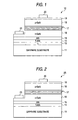
- FIG. 1 shows the configuration of the light-emitting diode 10.
- Layer Composition Dopant p-type layer 18 p-GaN : Mg
- Layer 17 containing light-emitting layer contains a layer of InGaN n-type layer 16 n-GaN : Si Buffer layer 15 AlN Metal nitride layer 14 Ti 0.97 Al 0.03 N Ti layer 13 Ti Substrate 11 sapphire
- the n-type layer 16 may be of a double-layered structure with an n- layer of a low electron density on the layer 17 containing a light-emitting layer side and an n+ layer of a high electron density on the buffer layer 15 side. The latter is called.”n-type contact layer”.
- the layer 17 containing a light-emitting layer is not limited to a superlattice structure.
- a single hetero type structure, a double hetero type structure, a homo-junction type structure, or the like, may be used as the structure of the light-emitting device.
- a single quantum well structure may be also used.
- the p-type layer 18 may be of a double-layered structure with a p- layer of a low hole density on the layer 17 containing a light-emitting layer side and a p+ layer of a high hole density on the electrode side.
- the latter is called "p-type contact layer”.
- the Ti layer 13 is formed on a face a of the sapphire substrate by a reactive DC magnetron sputtering method. While nitrogen is circulated, Al is added as a target so that the TiAlN layer 14 is formed on the Ti layer 13.by a reactive DC magnetron sputtering method. Incidentally, a TiAl alloy may be also used as the target. The target is further replaced by Al so that the AlN buffer layer 15 is formed by a reactive DC magnetron sputtering method. Incidentally, the formation of the AlN buffer layer 15 may be omitted.
- the sample of AlN/TiAlN/Ti/sapphire is transferred from a sputtering apparatus into a chamber of an MOCVD apparatus . While hydrogen gas and ammonia are circulated into the chamber, the sample is heated to 1100°C and kept for 5 minutes.
- the n-type layer 16 and Group III nitride compound semiconductor layers after the n-type layer 16 are formed by an ordinary method (MOCVD method) .
- MOCVD method an ammonia gas and gases of group III element alkyl compounds such as trimethylgallium (TMG), trimethylaluminum (TMA) and trimethylindium (TMI) are supplied onto a substrate heated to an appropriate temperature and are subjected to a heat decomposition reaction to thereby grow a desired crystal on the substrate.
- group III element alkyl compounds such as trimethylgallium (TMG), trimethylaluminum (TMA) and trimethylindium (TMI) are supplied onto a substrate heated to an appropriate temperature and are subjected to a heat decomposition reaction to thereby grow a desired crystal on the substrate.
- the group III nitride compound semiconductor layers 16 to 18 formed thus have good crystallinity.
- a transparent electrode 19 is constituted by a thin film containing gold.
- the transparent electrode 19 is laminated so as to cover the substantially whole upper surface of the p-type layer 18.
- a p-type electrode 20 is also constituted by a material containing gold.
- the p-type electrode 20 is formed on the transparent electrode 19 by vapor deposition.
- An n-type electrode 21 is formed by vapor deposition onto a surface of the n-GaN layer 16 exposed by etching.
- the AlN buffer layer 15 may be also formed by an MOCVD method.
- Fig. 2 shows a light-emitting diode 25 according to a second embodiment.
- parts the same as those in the first embodiment are referred to by numerals the same as those in the first embodiment and their description will be omitted.
- the light-emitting diode 25 according to this embodiment is configured so that the Ti layer 13 is omitted from the light-emitting diode shown in Fig. 1.
- the metal nitride layer 14 is formed directly on the sapphire substrate.
- Group III nitride compound semiconductor layers 16 to 18 of excellent crystallinity can be obtained.
- Fig. 3 shows a light-emitting diode 30 according to a third embodiment.
- parts the same as those in Fig. 2 are referred to by numerals the same as those in Fig. 2, and their description will be omitted.
- a configuration that an n-type electrode 21 is formed on the metal nitride layer 14 is applied to the light-emitting diode shown in Fig. 2.
- the metal nitride layer 14 has electrically conductive characteristic higher than that of the n-GaN. layer 16, an electric current can be distributed into the Group III nitride compound semiconductor layers more uniformly as a whole.
- the metal nitride layer 14 of TiAlN contains the same element (Al) as that of the n-type electrode 21, contact resistance can be reduced as well as the adhesion between the two can be improved.
- Fig. 4 shows a light-emitting diode 40 according to a fourth embodiment.
- Layer Composition Dopant p-type layer 18 p-GaN : Mg
- Layer 17 containing a light-emitting layer contains a layer of InGaN n-type layer 16 n-GaN : Si Buffer layer 15 AlN Metal nitride layer 14 Ti 0.97 Al 0.03 N Ti layer 13 Ti Substrate 11 silicon single crystal (111)
- the method of growing the TiN layer 13 et seq. formed on the (111) surface of Si is the same as that in the first embodiment.
- the Si substrate layer 41 can be used as an n-type electrode because it has electrically conductive characteristic.
- the AlN buffer layer 15 may be formed by an MOCVD method or need not be formed by the MOVCD method. Further, an Al layer with a film thickness of 10 nm (100 ⁇ ) may be formed between the Si substrate 41 and the Ti layer 13. The Ti layer 13 may be omitted.
- Fig. 5 shows a semiconductor device according to a fifth embodiment of the invention.
- the semiconductor device according to this embodiment is a light-emitting diode 50.
- parts the same as those in Fig. 4 are referred to by numerals the same as those in Fig. 4 and their description will be omitted.
- Layer Composition Dopant n-type layer 58 n-GaN : Si
- Layer 17 containing a light-emitting layer contains a layer of InGaN p-type layer 56 p-GaN : Mg Buffer layer 15 AlN
- Metal nitride layer 14 Ti 0.97 Al 0.03 N Ti layer 13 Ti Substrate 41 silicon single crystal (111)
- the p-type layer 56, the layer 17 containing a light-emitting layer and the n-type layer 58 are grown successively on the buffer layer 15 to thereby form the light-emitting diode 50.
- the transparent electrode see the reference numeral 19 in Fig. 4 can be dispensed with because the n-type layer 58 low in resistance value is used as the uppermost layer.
- the reference numeral 59 in the drawing designates an n-electrode.
- the Si substrate 41 can be directly used as a p-electrode.
- the AlN buffer layer 15 may be formed by an MOCVD method or need not be formed by the MOVCD method. Further, an Al layer with a film thickness of 10 nm (100 ⁇ ) may be formed between the Si substrate and Ti. The Ti layer 13 may be omitted.
- Fig. 6 shows a further embodiment of the invention.
- parts in Fig. 6 the same as those in the first embodiment are referred to by numerals the same as those in the first embodiment and their description will be omitted.
- the film thickness of a TiAlN layer 64 is made 80 ⁇ m.
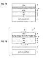
- Semiconductor layers 15 to 18 are formed on the TiAlN layer 64 by an MOCVD method (see Fig. 6A). Then, the Ti layer 13 is chemically etched with aqua regia to separate the substrate from the TiAlN layer 64 (see Fig. 6B) .
- Electrodes 19, 20 and 61 are formed by vapor deposition in the same manner as in the first embodiment to thereby obtain a light-emitting diode 60 according to this embodiment.
- the Ti layer 13 maybe removed after the semiconductor layers are partially formed.
- the Ti layer 13 may be removed by etching just after the TiAlN layer 64 is formed. That is, a substrate of TiAlN is obtained.
- the light-emitting diode 60 obtained thus has a bulk TiAlN substrate as its substrate. Because TiAlN has electrically conductive characteristic, the TiAlN substrate 64 per se may be used as an electrode. In addition, because TiAlN has a metallic gloss, light emitted from the layer containing a light-emitting layer can be efficiently reflected toward the emission observation surface side (the top side in the drawing) .
- Fig. 7 shows a further embodiment of the invention. Incidentally, parts the same as those in Fig. 6 are referred to by numerals the same as those in Fig. 6 and their description will be omitted.
- a p-type layer 76, a layer 17 containing a light-emitting layer and an n-type layer 78 are grown successively on the buffer layer 15 by an MOCVD method.
- the transparent electrode see the reference numeral 19 in Fig. 6
- the transparent electrode can be dispensed with because the n-type layer 78 low in resistance value is used as the uppermost layer.
- the Ti layer 13 is chemically etched with aqua regia to separate the substrate from the TiAlN layer 64 (see Fig. 7B).
- An electrode 79 is formed by vapor deposition in the same manner as in the fifth embodiment to thereby obtain a light-emitting diode 70 according to this embodiment.
- the Ti layer 13 may be removed after the semiconductor layers are partially formed.
- the Ti layer 13 may be removed by etching just after the TiAlN layer 64 is formed. That is, a substrate of TiAlN is obtained.
- the light-emitting diode 70 obtained thus has a bulk TiAlN substrate as its substrate. Because TiAlN has electrically conductive characteristic, the TiAlN substrate 64 per se may be used as an electrode. In addition, because TiAlN has a metallic gloss, light emitted from the layer containing a light-emitting layer can be efficiently reflected toward the emission observation surface side (the top side in the drawing) .
- the buffer layer is formed by a DC magnetron sputtering method
- it may be formed by an MOCVD method or the like (but the growth temperature is a high temperature of 1000°C).
- the device to which the present invention is applied is not limited to the aforementioned light-emitting diode.
- the present invention can be applied also to optical devices such as a photodetector, a laser diode, a solar cell, etc.; bipolar devices such as a rectifier, a thyristor, a transistor, etc.; unipolar devices such as an FET, etc.; and electronic devices such as a microwave device, etc.
- the present invention may be further applied to laminates which are intermediates of these devices.
- a Group III nitride compound semiconductor device having: a silicon substrate; a metal nitride layer formed on the silicon substrate and made of (Ti 1-x A x )N in which A is at least one kind of metal selected from the group consisting of Al, Ga, and In; and a Group III nitride compound semiconductor layer formed on the metal nitride layer.
- the metal A is Al and the composition x is 0.01 to 0.6.
- the Group III nitride compound semiconductor device can be used as a light-emitting device or a photodetector.
- a Group III nitride compound semiconductor device having: a sapphire substrate; a metal nitride layer formed on the sapphire substrate and made of (Ti 1-x A x )N in which A is at least one kind of metal selected from the group consisting of Al, Ga, and In; and a Group III nitride compound semiconductor layer formed on the metal nitride layer.
- the metal A is Al and the composition x is 0.01 to 0.6.
- the Group III nitride compound semiconductor device can be used as a light-emitting device or a photodetector.
- the metal nitride layer has electrically conductive characteristic, so that an n-electrode can be formed in a portion of the metal nitride layer exposed by etching of the Group III nitride compound semiconductor layers.
- a laminate having: a metal nitride layer made of (Ti 1-x A x )N in which A is at least one kind of metal selected from the group consisting of Al, Ga, and In; and a Group III nitride compound semiconductor layer formed on the metal nitride layer.
- the metal A is Al and the composition x is 0.01 to 0.6.
- a Ti layer may be provided between a substrate and the metal nitride layer.
- the laminate can be used as a light-emitting device or a photodetector.
- a method of producing a laminate having the steps of: forming a titanium layer on a substrate; forming a metal nitride layer on the titanium layer so that the metal nitride layer is made of (Ti 1-x A x )N in which A is at least one kind of metal selected from the group consisting of Al, Ga, and In; and forming a Group III nitride compound semiconductor layer on the metal nitride layer.
- the method may further have the step of separating the substrate from the metal nitride layer by chemically etching the titanium layer.
- the metal A is Al and the composition x is 0.01 to 0.6.
- the substrate may be preferably selected from the group consisting of sapphire, silicon carbide, gallium nitride, silicon, gallium phosphide, zirconium diboride, and gallium arsenide.
- a laminate having: a silicon substrate; a metal nitride layer formed on the silicon substrate and made of (Ti 1-x A x )N in which A is at least one kind of metal selected from the group consisting of Al, Ga,. and In; and a Group III nitride compound semiconductor layer formed on the metal nitride layer.
- the metal A is Al and the composition x is 0.01 to 0.6.
- the.laminate can be used as a light-emitting device or a photodetector.
- a laminate having: a sapphire substrate; ametal nitride layer formed on the sapphire substrate and made of (Ti 1-x A x )N in which A is at least one kind of metal selected from the group consisting of Al, Ga, and In; and a Group III nitride compound semiconductor layer formed on the metal nitride layer.
- the metal A is Al and the composition x is 0.01 to 0.6.
- the laminate can be used as a light-emitting device or a photodetector.
- the metal nitride layer has electrically conductive characteristic, so that an n-electrode can be formed in a portion of the metal nitride layer exposed by etching of the Group III nitride compound semiconductor layers.
Landscapes
- Led Devices (AREA)
- Light Receiving Elements (AREA)
- Semiconductor Lasers (AREA)
- Formation Of Insulating Films (AREA)
Abstract
Description
| Layer | Composition : Dopant |
| p-type layer 18 | p-GaN : |
| Layer | |
| 17 containing light-emitting layer | contains a layer of InGaN |
| n-type layer 16 | n-GaN : |
| Buffer layer | |
| 15 | AlN |
| | Ti0.97Al0.03 |
| Ti layer | |
| 13 | |
| Substrate | |
| 11 | sapphire |
| Layer | Composition : Dopant |
| p-type layer 18 | p-GaN : |
| Layer | |
| 17 containing a light-emitting layer | contains a layer of InGaN |
| n-type layer 16 | n-GaN : |
| Buffer layer | |
| 15 | AlN |
| | Ti0.97Al0.03 |
| Ti layer | |
| 13 | |
| Substrate | |
| 11 | silicon single crystal (111) |
| Layer | Composition : Dopant |
| n-type layer 58 | n-GaN : |
| Layer | |
| 17 containing a light-emitting layer | contains a layer of InGaN |
| p-type layer 56 | p-GaN : |
| Buffer layer | |
| 15 | AlN |
| | Ti0.97Al0.03 |
| Ti layer | |
| 13 | |
| Substrate | |
| 41 | silicon single crystal (111) |
Claims (10)
- A Group III nitride compound semiconductor device comprising:a metal nitride layer made of (Ti1-xAx)N in which A is at least one kind of metal selected from the group consisting of Al, Ga, and In; anda Group III nitride compound semiconductor layer formed on said metal nitride layer.
- A Group III nitride compound semiconductor device according to claim 1, wherein said metal A is Al.
- A Group III nitride compound semiconductor device according to claim 1, wherein a composition x of said metal A is 0.01 to 0.6.
- A Group III nitride compound semiconductor device according to claim 1, further comprising a substrate, and a Ti layer formed between said substrate and said metal nitride layer.
- A Group III nitride compound semiconductor device according to claim 1, wherein said Group III nitride compound semiconductor device is a light-emitting device or a photodetector.
- A method of producing a Group III nitride compound semiconductor device, comprising steps of:forming a titanium layer on a substrate;forming a metal nitride layer on said titanium layer so that said metal nitride layer is made of (Ti1-xAx)N in which A is at least one kind of metal selected from the group consisting of Al, Ga, and In; andforming a Group III nitride compound semiconductor layer on said metal nitride layer.
- A method of producing a Group III nitride compound semiconductor device according to claim 6, further comprising. a step of separating said substrate from said metal nitride layer by chemically etching said titanium layer.
- A method of producing a Group III nitride compound semiconductor device according to claim 6, wherein said metal A is Al.
- A method of producing a Group III nitride compound semiconductor device according to claim 6, wherein a composition x of said metal A is 0.01 to 0.6.
- A method of producing a Group III nitride compound semiconductor device according to claim 6, wherein said substrate is one member selected from the group consisting of sapphire, silicon carbide, gallium nitride, silicon, gallium phosphide, zirconium diboride, and gallium arsenide.
Applications Claiming Priority (3)
| Application Number | Priority Date | Filing Date | Title |
|---|---|---|---|
| JP2001007038A JP4710139B2 (en) | 2001-01-15 | 2001-01-15 | Group III nitride compound semiconductor device |
| JP2001007038 | 2001-01-15 | ||
| PCT/JP2002/000098 WO2002056393A1 (en) | 2001-01-15 | 2002-01-10 | Compound semiconductor element based on group iii element nitride |
Publications (2)
| Publication Number | Publication Date |
|---|---|
| EP1361616A1 true EP1361616A1 (en) | 2003-11-12 |
| EP1361616A4 EP1361616A4 (en) | 2007-04-04 |
Family
ID=18874844
Family Applications (1)
| Application Number | Title | Priority Date | Filing Date |
|---|---|---|---|
| EP02715722A Withdrawn EP1361616A4 (en) | 2001-01-15 | 2002-01-10 | COMPOUND NITRIDE COMPOUND SEMICONDUCTOR ELEMENT OF GROUP III OF ELEMENTS |
Country Status (7)
| Country | Link |
|---|---|
| US (1) | US7312472B2 (en) |
| EP (1) | EP1361616A4 (en) |
| JP (1) | JP4710139B2 (en) |
| KR (1) | KR100532645B1 (en) |
| CN (1) | CN1254868C (en) |
| TW (1) | TW571446B (en) |
| WO (1) | WO2002056393A1 (en) |
Cited By (4)
| Publication number | Priority date | Publication date | Assignee | Title |
|---|---|---|---|---|
| US6897139B2 (en) * | 2000-07-19 | 2005-05-24 | Toyoda Gosei Co., Ltd. | Group III nitride compound semiconductor device |
| EP1821348A3 (en) * | 2006-02-16 | 2010-09-08 | LG Electronics Inc. | Light emitting device having vertical structure package thereof and method for manufacturing the same |
| EP1930486A4 (en) * | 2005-08-25 | 2014-01-01 | Tohoku Techno Arch Co Ltd | PROCESS FOR PRODUCING SEMICONDUCTOR SUBSTRATE |
| FR3112238A1 (en) * | 2020-07-06 | 2022-01-07 | Saint-Gobain Lumilog | SEMICONDUCTOR SUBSTRATE WITH NITRURED INTERFACE LAYER |
Families Citing this family (25)
| Publication number | Priority date | Publication date | Assignee | Title |
|---|---|---|---|---|
| JP4766845B2 (en) * | 2003-07-25 | 2011-09-07 | シャープ株式会社 | Nitride-based compound semiconductor light-emitting device and method for manufacturing the same |
| JP4667096B2 (en) * | 2005-03-25 | 2011-04-06 | 株式会社半導体エネルギー研究所 | Organic semiconductor device and manufacturing method thereof |
| KR100753152B1 (en) * | 2005-08-12 | 2007-08-30 | 삼성전자주식회사 | Nitride-based light emitting device and its manufacturing method |
| US7932539B2 (en) * | 2005-11-29 | 2011-04-26 | The Hong Kong University Of Science And Technology | Enhancement-mode III-N devices, circuits, and methods |
| US8044432B2 (en) * | 2005-11-29 | 2011-10-25 | The Hong Kong University Of Science And Technology | Low density drain HEMTs |
| US7972915B2 (en) * | 2005-11-29 | 2011-07-05 | The Hong Kong University Of Science And Technology | Monolithic integration of enhancement- and depletion-mode AlGaN/GaN HFETs |
| JP2007246331A (en) * | 2006-03-15 | 2007-09-27 | Hitachi Cable Ltd | III-V nitride semiconductor substrate and method for manufacturing the same |
| JP4884866B2 (en) * | 2006-07-25 | 2012-02-29 | 三菱電機株式会社 | Manufacturing method of nitride semiconductor device |
| JP5049659B2 (en) * | 2007-06-11 | 2012-10-17 | 昭和電工株式会社 | Group III nitride semiconductor manufacturing method, group III nitride semiconductor light emitting device manufacturing method, group III nitride semiconductor light emitting device, and lamp |
| US8502323B2 (en) * | 2007-08-03 | 2013-08-06 | The Hong Kong University Of Science And Technology | Reliable normally-off III-nitride active device structures, and related methods and systems |
| KR101457208B1 (en) * | 2007-09-21 | 2014-10-31 | 서울바이오시스 주식회사 | Group ⅲ nitride compound semiconductor device |
| US8076699B2 (en) * | 2008-04-02 | 2011-12-13 | The Hong Kong Univ. Of Science And Technology | Integrated HEMT and lateral field-effect rectifier combinations, methods, and systems |
| US7875534B2 (en) * | 2008-07-21 | 2011-01-25 | Taiwan Semiconductor Manufacturing Company, Ltd. | Realizing N-face III-nitride semiconductors by nitridation treatment |
| US20100084687A1 (en) * | 2008-10-03 | 2010-04-08 | The Hong Kong University Of Science And Technology | Aluminum gallium nitride/gallium nitride high electron mobility transistors |
| US8409895B2 (en) * | 2010-12-16 | 2013-04-02 | Applied Materials, Inc. | Gallium nitride-based LED fabrication with PVD-formed aluminum nitride buffer layer |
| KR101761309B1 (en) * | 2011-04-19 | 2017-07-25 | 삼성전자주식회사 | GaN film structure, method of fabricating the same and semiconductor device including the same |
| CN102522505B (en) * | 2012-01-14 | 2014-08-20 | 西安电子科技大学 | Inorganic and organic hybrid solar cell |
| US9929310B2 (en) | 2013-03-14 | 2018-03-27 | Applied Materials, Inc. | Oxygen controlled PVD aluminum nitride buffer for gallium nitride-based optoelectronic and electronic devices |
| US9515226B2 (en) * | 2013-07-10 | 2016-12-06 | Yangang Xi | Light emitting device and method for making the same |
| US10418522B2 (en) | 2016-12-20 | 2019-09-17 | Goforward Technology Inc. | Optoelectronic device and method for making the same |
| US10535739B2 (en) * | 2017-04-24 | 2020-01-14 | Enkris Semiconductor, Inc | Semiconductor structure and method of preparing semiconductor structure |
| JP7081551B2 (en) * | 2019-03-28 | 2022-06-07 | 日本電信電話株式会社 | Avalanche photodiode and its manufacturing method |
| US10971650B2 (en) * | 2019-07-29 | 2021-04-06 | Lextar Electronics Corporation | Light emitting device |
| CN112086542B (en) * | 2020-07-27 | 2021-11-05 | 华灿光电(苏州)有限公司 | Light-emitting diode epitaxial wafer and growth method thereof |
| WO2025089116A1 (en) * | 2023-10-27 | 2025-05-01 | 国立研究開発法人物質・材料研究機構 | Base structure for vertical semiconductor devices, use of same, and method for manufacturing same |
Family Cites Families (23)
| Publication number | Priority date | Publication date | Assignee | Title |
|---|---|---|---|---|
| JP3404813B2 (en) * | 1992-09-04 | 2003-05-12 | 住友電気工業株式会社 | Aluminum nitride sintered body and method for producing the same |
| JP3675003B2 (en) * | 1995-10-27 | 2005-07-27 | 昭和電工株式会社 | Semiconductor light emitting device |
| US5874747A (en) * | 1996-02-05 | 1999-02-23 | Advanced Technology Materials, Inc. | High brightness electroluminescent device emitting in the green to ultraviolet spectrum and method of making the same |
| JP3779766B2 (en) * | 1996-02-29 | 2006-05-31 | シャープ株式会社 | III-V compound semiconductor device |
| JP3363740B2 (en) * | 1997-03-12 | 2003-01-08 | 三洋電機株式会社 | Electrode and semiconductor device of nitride compound semiconductor |
| JPH10270802A (en) * | 1997-03-25 | 1998-10-09 | Sharp Corp | Nitride III-V compound semiconductor device and method of manufacturing the same |
| JPH10321954A (en) * | 1997-05-15 | 1998-12-04 | Fuji Electric Co Ltd | Group III nitride semiconductor device and method of manufacturing the same |
| JP3822318B2 (en) * | 1997-07-17 | 2006-09-20 | 株式会社東芝 | Semiconductor light emitting device and manufacturing method thereof |
| JP3517867B2 (en) * | 1997-10-10 | 2004-04-12 | 豊田合成株式会社 | GaN-based semiconductor devices |
| US5952681A (en) * | 1997-11-24 | 1999-09-14 | Chen; Hsing | Light emitting diode emitting red, green and blue light |
| RU2186447C2 (en) | 1997-11-28 | 2002-07-27 | Котелянский Иосиф Моисеевич | Semiconductor device |
| JP3028809B2 (en) | 1998-05-08 | 2000-04-04 | サンケン電気株式会社 | Method for manufacturing semiconductor light emitting device |
| JP2000049092A (en) * | 1998-05-29 | 2000-02-18 | Matsushita Electron Corp | Method for growing crystal of nitride semiconductor, nitride semiconductor device, and manufacture of the device |
| JP2000077712A (en) * | 1998-08-31 | 2000-03-14 | Sanken Electric Co Ltd | Semiconductor light emitting element |
| JP3019085B1 (en) * | 1998-10-09 | 2000-03-13 | サンケン電気株式会社 | Semiconductor light emitting device and method of manufacturing the same |
| JP2000243947A (en) * | 1999-02-19 | 2000-09-08 | Sharp Corp | Nitride compound semiconductor device |
| US6426512B1 (en) * | 1999-03-05 | 2002-07-30 | Toyoda Gosei Co., Ltd. | Group III nitride compound semiconductor device |
| JP3453544B2 (en) | 1999-03-26 | 2003-10-06 | キヤノン株式会社 | Manufacturing method of semiconductor member |
| JP2000286445A (en) * | 1999-03-31 | 2000-10-13 | Toyoda Gosei Co Ltd | Group III nitride compound semiconductor light emitting device |
| JP3760663B2 (en) * | 1999-03-31 | 2006-03-29 | 豊田合成株式会社 | Method for producing group III nitride compound semiconductor device |
| JP4433356B2 (en) * | 1999-07-09 | 2010-03-17 | シャープ株式会社 | Semiconductor laser element and optical information reproducing apparatus |
| TW439304B (en) * | 2000-01-05 | 2001-06-07 | Ind Tech Res Inst | GaN series III-V compound semiconductor devices |
| JP3963068B2 (en) * | 2000-07-19 | 2007-08-22 | 豊田合成株式会社 | Method for producing group III nitride compound semiconductor device |
-
2001
- 2001-01-15 JP JP2001007038A patent/JP4710139B2/en not_active Expired - Fee Related
-
2002
- 2002-01-10 EP EP02715722A patent/EP1361616A4/en not_active Withdrawn
- 2002-01-10 WO PCT/JP2002/000098 patent/WO2002056393A1/en not_active Ceased
- 2002-01-10 CN CNB028037537A patent/CN1254868C/en not_active Expired - Fee Related
- 2002-01-10 US US10/466,185 patent/US7312472B2/en not_active Expired - Fee Related
- 2002-01-10 KR KR10-2003-7009406A patent/KR100532645B1/en not_active Expired - Fee Related
- 2002-01-15 TW TW091100454A patent/TW571446B/en not_active IP Right Cessation
Cited By (12)
| Publication number | Priority date | Publication date | Assignee | Title |
|---|---|---|---|---|
| US6897139B2 (en) * | 2000-07-19 | 2005-05-24 | Toyoda Gosei Co., Ltd. | Group III nitride compound semiconductor device |
| EP1930486A4 (en) * | 2005-08-25 | 2014-01-01 | Tohoku Techno Arch Co Ltd | PROCESS FOR PRODUCING SEMICONDUCTOR SUBSTRATE |
| EP1821348A3 (en) * | 2006-02-16 | 2010-09-08 | LG Electronics Inc. | Light emitting device having vertical structure package thereof and method for manufacturing the same |
| US7928462B2 (en) | 2006-02-16 | 2011-04-19 | Lg Electronics Inc. | Light emitting device having vertical structure, package thereof and method for manufacturing the same |
| US8546837B2 (en) | 2006-02-16 | 2013-10-01 | Lg Electronics Inc. | Light emitting device having vertical structure, package thereof and method for manufacturing the same |
| US8729595B2 (en) | 2006-02-16 | 2014-05-20 | Lg Electronics Inc. | Light emitting device having vertical structure and package thereof |
| US9312459B2 (en) | 2006-02-16 | 2016-04-12 | Lg Electronics Inc. | Light emitting device having vertical structure and package thereof |
| US9679973B2 (en) | 2006-02-16 | 2017-06-13 | Lg Electronics Inc. | Light emitting device having vertical structure and package thereof |
| US9812531B2 (en) | 2006-02-16 | 2017-11-07 | Lg Electronics Inc. | Light emitting device having vertical structure and package thereof |
| FR3112238A1 (en) * | 2020-07-06 | 2022-01-07 | Saint-Gobain Lumilog | SEMICONDUCTOR SUBSTRATE WITH NITRURED INTERFACE LAYER |
| WO2022008836A1 (en) * | 2020-07-06 | 2022-01-13 | Saint-Gobain Lumilog | Semiconductor substrate with nitrided interface layer |
| US12506003B2 (en) | 2020-07-06 | 2025-12-23 | Ivworks Co., Ltd. | Semiconductor substrate with nitride interface layer |
Also Published As
| Publication number | Publication date |
|---|---|
| EP1361616A4 (en) | 2007-04-04 |
| JP4710139B2 (en) | 2011-06-29 |
| JP2002217452A (en) | 2002-08-02 |
| KR20030069212A (en) | 2003-08-25 |
| US20040079949A1 (en) | 2004-04-29 |
| US7312472B2 (en) | 2007-12-25 |
| CN1486513A (en) | 2004-03-31 |
| CN1254868C (en) | 2006-05-03 |
| KR100532645B1 (en) | 2005-12-01 |
| TW571446B (en) | 2004-01-11 |
| WO2002056393A1 (en) | 2002-07-18 |
Similar Documents
| Publication | Publication Date | Title |
|---|---|---|
| US7312472B2 (en) | Compound semiconductor element based on Group III element nitride | |
| US6897139B2 (en) | Group III nitride compound semiconductor device | |
| US6875629B2 (en) | III group nitride based semiconductor element and method for manufacture thereof | |
| US6426512B1 (en) | Group III nitride compound semiconductor device | |
| US7576363B2 (en) | Group III nitride compound semiconductor light emitting device | |
| US7749785B2 (en) | Manufacturing method of group III nitride semiconductor light-emitting device | |
| US7521269B2 (en) | Single-crystal nitride-based semiconductor substrate and method of manufacturing high-quality nitride-based light emitting device by using the same | |
| US7795050B2 (en) | Single-crystal nitride-based semiconductor substrate and method of manufacturing high-quality nitride-based light emitting device by using the same | |
| JP2001094150A (en) | Group iii nitride compound semiconductor element | |
| JP3702721B2 (en) | Group III nitride compound semiconductor device | |
| US6921923B1 (en) | Group III nitride compound semiconductor device | |
| JP2004096133A (en) | Group-iii nitride based compound semiconductor device | |
| JP2003017412A (en) | Method of manufacturing iii nitride compound semiconductor element | |
| JP2003060229A (en) | Semiconductor light-emitting element and manufacturing method therefor | |
| KR20050092365A (en) | Boron phosphide-based compound semiconductor device, production method thereof and light-emitting diode | |
| JP2005183780A (en) | Manufacturing method of nitride-based iii group compound semiconductor light emitting element |
Legal Events
| Date | Code | Title | Description |
|---|---|---|---|
| PUAI | Public reference made under article 153(3) epc to a published international application that has entered the european phase |
Free format text: ORIGINAL CODE: 0009012 |
|
| 17P | Request for examination filed |
Effective date: 20030710 |
|
| AK | Designated contracting states |
Kind code of ref document: A1 Designated state(s): AT BE CH CY DE DK ES FI FR GB GR IE IT LI LU MC NL PT SE TR |
|
| AX | Request for extension of the european patent |
Extension state: AL LT LV MK RO SI |
|
| RBV | Designated contracting states (corrected) |
Designated state(s): AT BE CH DE FR GB LI |
|
| A4 | Supplementary search report drawn up and despatched |
Effective date: 20070301 |
|
| RIC1 | Information provided on ipc code assigned before grant |
Ipc: C30B 29/40 20060101ALI20070223BHEP Ipc: H01L 21/205 20060101ALI20070223BHEP Ipc: H01L 21/203 20060101ALI20070223BHEP Ipc: H01L 33/00 20060101ALI20070223BHEP Ipc: H01L 21/20 20060101AFI20070223BHEP |
|
| 17Q | First examination report despatched |
Effective date: 20070531 |
|
| STAA | Information on the status of an ep patent application or granted ep patent |
Free format text: STATUS: THE APPLICATION IS DEEMED TO BE WITHDRAWN |
|
| 18D | Application deemed to be withdrawn |
Effective date: 20100803 |