EP1359630A2 - Semiconducting hole injection materials for organic light emitting devices - Google Patents
Semiconducting hole injection materials for organic light emitting devices Download PDFInfo
- Publication number
- EP1359630A2 EP1359630A2 EP03252295A EP03252295A EP1359630A2 EP 1359630 A2 EP1359630 A2 EP 1359630A2 EP 03252295 A EP03252295 A EP 03252295A EP 03252295 A EP03252295 A EP 03252295A EP 1359630 A2 EP1359630 A2 EP 1359630A2
- Authority
- EP
- European Patent Office
- Prior art keywords
- charge transport
- light emitting
- organic light
- oxidant
- hole injection
- Prior art date
- Legal status (The legal status is an assumption and is not a legal conclusion. Google has not performed a legal analysis and makes no representation as to the accuracy of the status listed.)
- Withdrawn
Links
Images

Classifications
-
- H—ELECTRICITY
- H10—SEMICONDUCTOR DEVICES; ELECTRIC SOLID-STATE DEVICES NOT OTHERWISE PROVIDED FOR
- H10K—ORGANIC ELECTRIC SOLID-STATE DEVICES
- H10K71/00—Manufacture or treatment specially adapted for the organic devices covered by this subclass
- H10K71/30—Doping active layers, e.g. electron transporting layers
-
- H—ELECTRICITY
- H10—SEMICONDUCTOR DEVICES; ELECTRIC SOLID-STATE DEVICES NOT OTHERWISE PROVIDED FOR
- H10K—ORGANIC ELECTRIC SOLID-STATE DEVICES
- H10K85/00—Organic materials used in the body or electrodes of devices covered by this subclass
- H10K85/40—Organosilicon compounds, e.g. TIPS pentacene
-
- H—ELECTRICITY
- H10—SEMICONDUCTOR DEVICES; ELECTRIC SOLID-STATE DEVICES NOT OTHERWISE PROVIDED FOR
- H10K—ORGANIC ELECTRIC SOLID-STATE DEVICES
- H10K85/00—Organic materials used in the body or electrodes of devices covered by this subclass
- H10K85/60—Organic compounds having low molecular weight
- H10K85/631—Amine compounds having at least two aryl rest on at least one amine-nitrogen atom, e.g. triphenylamine
- H10K85/633—Amine compounds having at least two aryl rest on at least one amine-nitrogen atom, e.g. triphenylamine comprising polycyclic condensed aromatic hydrocarbons as substituents on the nitrogen atom
-
- H—ELECTRICITY
- H10—SEMICONDUCTOR DEVICES; ELECTRIC SOLID-STATE DEVICES NOT OTHERWISE PROVIDED FOR
- H10K—ORGANIC ELECTRIC SOLID-STATE DEVICES
- H10K85/00—Organic materials used in the body or electrodes of devices covered by this subclass
- H10K85/791—Starburst compounds
-
- H—ELECTRICITY
- H10—SEMICONDUCTOR DEVICES; ELECTRIC SOLID-STATE DEVICES NOT OTHERWISE PROVIDED FOR
- H10K—ORGANIC ELECTRIC SOLID-STATE DEVICES
- H10K50/00—Organic light-emitting devices
- H10K50/10—OLEDs or polymer light-emitting diodes [PLED]
- H10K50/14—Carrier transporting layers
-
- H—ELECTRICITY
- H10—SEMICONDUCTOR DEVICES; ELECTRIC SOLID-STATE DEVICES NOT OTHERWISE PROVIDED FOR
- H10K—ORGANIC ELECTRIC SOLID-STATE DEVICES
- H10K50/00—Organic light-emitting devices
- H10K50/10—OLEDs or polymer light-emitting diodes [PLED]
- H10K50/17—Carrier injection layers
-
- H—ELECTRICITY
- H10—SEMICONDUCTOR DEVICES; ELECTRIC SOLID-STATE DEVICES NOT OTHERWISE PROVIDED FOR
- H10K—ORGANIC ELECTRIC SOLID-STATE DEVICES
- H10K85/00—Organic materials used in the body or electrodes of devices covered by this subclass
- H10K85/60—Organic compounds having low molecular weight
- H10K85/631—Amine compounds having at least two aryl rest on at least one amine-nitrogen atom, e.g. triphenylamine
-
- Y—GENERAL TAGGING OF NEW TECHNOLOGICAL DEVELOPMENTS; GENERAL TAGGING OF CROSS-SECTIONAL TECHNOLOGIES SPANNING OVER SEVERAL SECTIONS OF THE IPC; TECHNICAL SUBJECTS COVERED BY FORMER USPC CROSS-REFERENCE ART COLLECTIONS [XRACs] AND DIGESTS
- Y10—TECHNICAL SUBJECTS COVERED BY FORMER USPC
- Y10S—TECHNICAL SUBJECTS COVERED BY FORMER USPC CROSS-REFERENCE ART COLLECTIONS [XRACs] AND DIGESTS
- Y10S428/00—Stock material or miscellaneous articles
- Y10S428/917—Electroluminescent
-
- Y—GENERAL TAGGING OF NEW TECHNOLOGICAL DEVELOPMENTS; GENERAL TAGGING OF CROSS-SECTIONAL TECHNOLOGIES SPANNING OVER SEVERAL SECTIONS OF THE IPC; TECHNICAL SUBJECTS COVERED BY FORMER USPC CROSS-REFERENCE ART COLLECTIONS [XRACs] AND DIGESTS
- Y10—TECHNICAL SUBJECTS COVERED BY FORMER USPC
- Y10T—TECHNICAL SUBJECTS COVERED BY FORMER US CLASSIFICATION
- Y10T428/00—Stock material or miscellaneous articles
- Y10T428/26—Web or sheet containing structurally defined element or component, the element or component having a specified physical dimension
Definitions
- the present invention relates to oxidized charge transport materials which can form stable hole injection layers in organic light emitting devices without utilizing a polymeric binder.
- OLEDs typically comprise a layer of emissive material between an anode and a cathode.
- a bias is applied across the electrodes, positive charges (holes) and negative charges (electrons) are respectively injected from the anode and cathode into the emissive layer.
- the holes and the electrons form excitons in the emissive layer to emit light.
- Electrodes are chosen to facilitate charge injection.
- An indium-tin-oxide (ITO) anode has a relatively high work function and is therefore suitable for use as a hole injection electrode, while low work function metals such as Al, Mg and Ca are suitable for injection of electrons.
- OLED oxidized charge transport
- OTLs oxidized transport layers
- Conventional OTLs typically comprise a three-component coating: a charge transport molecule, an oxidized charge transport molecule, and a polymer binder.
- Different oxidant and charge transport molecule/polymer combinations have been developed and investigated for a wide range of applications. For example, U.S. Patent No.
- TPD N,N'-diphenyl-N,N'-bis(3-methylphenyl)-1,1'-biphenyl-4,4'-diamine
- oxidizing reagents such as I 2 , FeCl 3 , SbCl 5 and tris(4-bromophenyl)aminium hexachloroantimonate (TBAHA)
- a drawback of the known OTL systems is that they are unstable and cannot readily be incorporated into a device without utilizing a polymeric binder.
- TM-TPD.SbF 6 N,N,N',N'-tetra-p-tolyl-4,4'-biphenyldiamine
- the invention is an oxidized transport material formed substantially without a polymeric binder suitable for use as a hole injection layer in an OLED, comprising a charge transport compound having more than two triarylamine groups, or having at least one triarylamine group and at least one fluorene group; and an oxidant complexed with said charge transport compound, wherein a portion of said charge transport compound is not complexed to the oxidant.
- oxidant is present in the oxidized charge transport material in an amount between 0.2 and 20 percent by weight.
- the oxidized transport material comprising the specified charge transport compounds is preferably fabricated as a thin layer in an organic light emitting device by solution processing, such as spin coating, without using a polymeric binder.
- Such layer generally has a thickness of about 50 Angstroms to about 50,000 Angstroms, preferably about 100 Angstroms to about 2,000 Angstroms. It is believed that the high molecular weight of the oligomeric charge transport compounds according to the invention provides these compounds with good film forming properties such that no polymeric binder is needed.
- the invention is an organic light emitting device comprising an anode and a cathode with an emissive layer interposed between them, and between the anode and the emissive layer, a hole injection layer consisting essentially of charge transport compound having more than two triarylamine groups, or having at least one triarylamine group and at least one fluorene group; complexed with an oxidant, wherein a portion of said charge transport compound is not complexed with said oxidant.
- Figure 1 is a schematic cross-sectional view of an EL device according to the invention.
- Devices according to the invention find use in display applications such as television screens, computer screens and image bar components for digital copiers and printers, although the invention is not limited to these uses.
- Figure 1 schematically depicts an OLED, including transparent substrate 1, anode 2 adjacent the substrate, a hole injection layer 3 comprising an OTL according to the invention adjacent the anode, emissive layer 4, optional electron transport layer 5 adjacent the emissive layer, and cathode 6.
- Each of these layers may itself comprise multiple layers of material having similar composition or function.
- Charge blocking layers (not shown) may also be used as known in the art.
- Functional layers may also be combined.
- an emissive layer may be adapted to exhibit electron transport properties.
- Optional functional layers can be interposed between any two functional layers 1 through 6 without departing from the scope of the invention.
- a buffer layer can be provided between the electrodes and the adjacent charge transfer layers to suppress leakage currents.
- OLEDs according to the invention may have a driving voltage between 0.1 V and 100 V, preferably between 1 V and 15 V, producing a current density at the anode/hole injection layer interface in a range of about 0.01 mA / cm 2 to about 1000 mA / cm 2 .
- Suitable materials for substrate 1 include glass, quartz and the like, and polymers (including, without limitation, polyesters, polycarbonates, polyacrylates, polymethacrylates, and polysulfones).
- the thickness of the substrate is not critical and can range, for example, from about 25 to over 1,000 microns, depending on the structural demands of the device.
- the anode adjacent the substrate can be comprised of a metal, an alloy, an electroconducting compound, or mixtures thereof, with a work function equal to or greater than about 4.0 electron volts.
- anodes include hole injecting electrodes such as indium tin oxide (ITO), tin oxide, zinc oxide, gold, platinum, electrically conductive carbon, and conjugated polymers such as polyaniline, polypyrrole, and the like. ITO is preferred, as it has good transparency in visible light.
- the thickness of the anode can range anywhere from about 10 nanometers to 1 micron.
- An OTL can be deposited adjacent the anode by vacuum deposition or solvent processing such as spin coating.
- the preferred method is spin coating. Accordingly, preferred charge transport compounds have good film forming properties so that they can be spin coated to the desired thickness.
- a charge transport compound can be selected from triarylamine charge transport compounds.
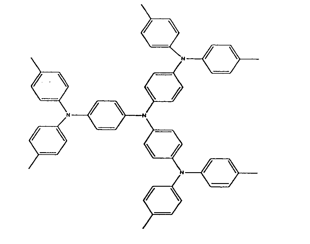
- Preferred triarylamine compounds are oligomeric, incorporating at least three triarylamine groups, as in Figure (I):
- oligomeric triarylamine charge transport compounds may incorporate one or more fluorene groups, and may be selected from Formulas (II) and (III), without limitation:
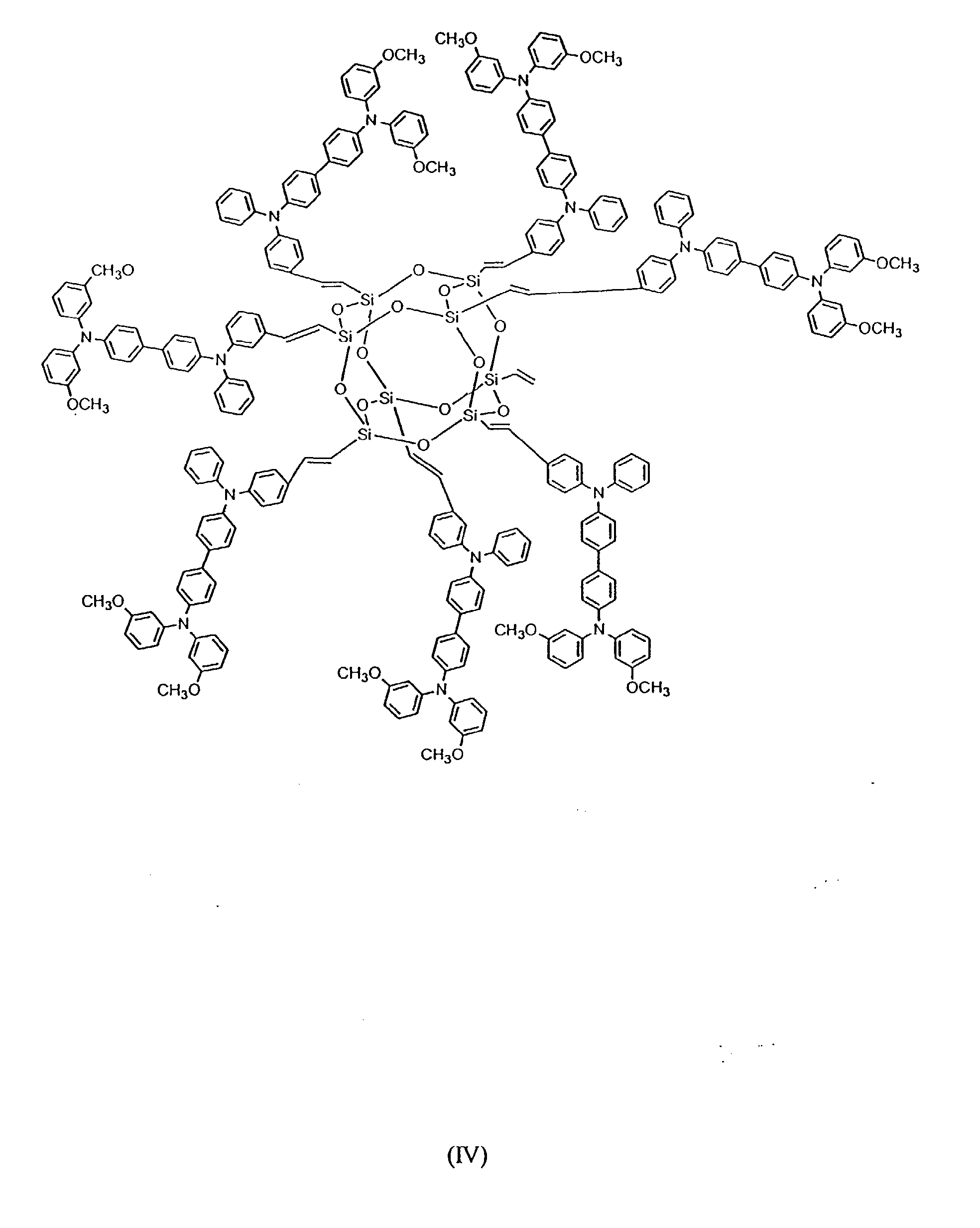
- between 2 and 8 hole-transporting aromatic amine groups may be incorporated onto a polyhedral silsesquioxane core moiety.
- Formulas (IV) and (V) below are exemplary of such an embodiment:
- Still other charge transport compounds within the scope of the invention are selected from compounds which can be formed into a thin film in an OLED and which possess hole transport properties, including: oligothiophenes, tetraselenotetracenes, mono- and oligo- tetrathiafulvalenes, oligo-tetraselenotetracenes and oligometallocenes.
- Other suitable charge transport compounds which may be oxidized to form the thin-layer oxidized charge transport materials of the invention can be selected from those disclosed in the aforementioned U.S. Patent No. 5,853,906.
- an oxidant which complexes with the charge transport compound to form an oxidized charge transport compound.
- any suitable oxidant may be used, including without limitation, I 2 , FeCl 3 , TBAHA, perfluoroacids, organic sulfonic acids, and Lewis acids.
- Lewis acids are preferred.
- the oxidant is selected from M m X n , where M is a metal selected from As, Sb, Au, Bi and P, and X is a halogen selected from F, Cl, and Br, and m and n are integers consistent with the valencies of the respective metal and halogen.
- the most preferred oxidant species are SbF 6 - , AuCl 4 - , and AsF 6 - .
- Oxidant includes both the oxidizing species, such as the Lewis acid used to oxidize the charge transport compound, and the charged species complexed with the charge transport compound.
- the weight percentage ratio of oxidant in the charge transport material is generally about 0.2 percent by weight to about 20 percent by weight (wt/wt) with respect to the charge transport material, and preferably between about 0.5 percent by weight and about 10.0 percent by weight.
- An advantage of the present invention is that suitably thick and robust hole injection layers can be fabricated without a polymeric binder.
- the thickness of the OTL ranges from about 50 Angstroms to about 50,000 Angstroms, preferably from about 100 Angstroms to about 2,000 Angstroms.
- Very thin film hole injection layers, less than about 50 Angstroms, have been used to lower device driving voltages. However, these very thin films can develop pinholes, leading to device instability. On the other hand, films that are too thick may lead to high driving voltages.
- Suitable luminescent materials for use in an OLED according to the invention include those formed of a conjugated organic host material, such as naphthalene, anthracene, phenanthrene, pyrene, benzopyrene, chrysene, picene, carbazole, fluorene, biphenyl, terphenyls, quarterphenyls, triphenylene oxide, dihalobiphenyl, trans-stilbene, and 1,4-diphenylbutadiene combined with a conjugated organic activating agent having condensed benzene rings, such as anthracene, tetracene, and pentacene.
- a conjugated organic host material such as naphthalene, anthracene, phenanthrene, pyrene, benzopyrene, chrysene, picene, carbazole, fluorene, biphenyl, terphenyls, quarterphenyls, triphenylene oxide
- Combined electron transport/luminescent layers such as tetraphenylbutadiene in polystyrene, and 4,4'-bis(5,7-di-t-pentyl-2-benzoxazolyl)-stilbene may also be used as a luminescent layer in an OLED according to the present invention.
- the reaction product of poly(N-vinyl carbazole) (PVCz) with a strong oxidizing agent, such as SbCl 5 and the like, have also been demonstrated to exhibit luminescent and semiconducting characteristics and may be formed into a film and used in an OLED according to the invention.
- emissive layers in OLEDs include tris(8-hydroxyquinolate)aluminum (AlQ 3 ) complexes.
- AlQ 3 tris(8-hydroxyquinolate)aluminum
- Other metal complexes with heteroaromatic ligands such as those disclosed in U.S. Patent No. 5,925,472 (herein incorporated by reference), may also be used to form a luminescent layer in an OLED according to the invention.
- This list of potential luminescent layers is not exhaustive and many other alternative luminescent layers, hole-transport/luminescent layers, and electron-transport/luminescent layers, both currently available and being developed, can be used in an OLED according to the invention, as would be appreciated by those of skill in the art.
- emissive is meant radiation emitting and “luminescent” means visible light emitting, whether due to an applied bias or otherwise.
- an emissive layer and luminescent layer are used interchangeably. Accordingly an emissive layer is understood to include a hole transport/emissive layer and an electron transport/emissive layer.
- Any electron injecting, electron transport, and electron transport/luminescent, hole transport/luminescent, charge blocking, or buffer layer known to be useful in OLED manufacture may be employed in an OLED according to the invention.
- thin films of hole injection material suitable for use in an OLED can be made substantially without polymeric binder.
- substantially without polymeric binder is meant that a stable, thin film layer can be formed without use of an inert, non-conductive polymer.
- polymeric resins used to facilitate formation of thin films in OLEDs are disclosed in U.S. Patent No. 4,338,222, herein incorporated by reference.
- inert, non-conductive resins include polycarbonates, polystyrene, polyolefins, polyesters, polyamides, polyacrylates, and polymethacrylates.
- “Substantially without” does not exclude small amounts of the foregoing inert, nonconductive polymers in a hole injection layer.
- “Substantially without” simply means that there is less than an amount necessary to impart film forming properties to a material that otherwise could not be deposited in a stable thin film in an OLED.
- the hole injection layer does not include any polymer (or any compound having more than 10 repeat units) at all.
- other layers in the OLED may include polymers.
- star-cube a star-cube charge transport compound having the structure shown in Formula (V) (1kg) and AgSbF 6 (50 g) were dissolved in dichloromethane (1L) and stirred for 4 hours. The black solution was filtered to remove the Ag particles. The filtrate was then dried under reduced pressure to form the black powder, star-cube•SbF 6 , with a yield of 92%.
- a device was prepared using the above star-cube•SbF 6 material by dissolving 200 mg of star-cube•SbF 6 in 1,2-dichlorobenzene (20 ml) to form a solution which is then filtered with a filter having a pore size less than 1.0 ⁇ m.
- the solution is spin-coated on a clean ITO glass substrate with a spin speed of 4,000 rpm to obtain a thin OTL coating of 50 nm.
- An emissive layer of AlQ3 (thickness of 80 nm) is then evaporated on top of the OTL layer.
- the AlQ3 emissive layer On top of the AlQ3 emissive layer is deposited a thin layer of Li (5 nm) and then an Al layer (180 nm) as a cathode.
- the device shows bright green electroluminescence under a bias voltage of 3.0 V.
- the device manufactured according to this process has lowered turn-on voltage than an otherwise similar device using a star-cube hole transport layer without SbF 6 as the oxidizing dopant, which exhibits a turn-on voltage of 4.5 V.
Landscapes
- Engineering & Computer Science (AREA)
- Chemical & Material Sciences (AREA)
- Materials Engineering (AREA)
- Manufacturing & Machinery (AREA)
- Physics & Mathematics (AREA)
- Spectroscopy & Molecular Physics (AREA)
- Electroluminescent Light Sources (AREA)
Abstract
Description

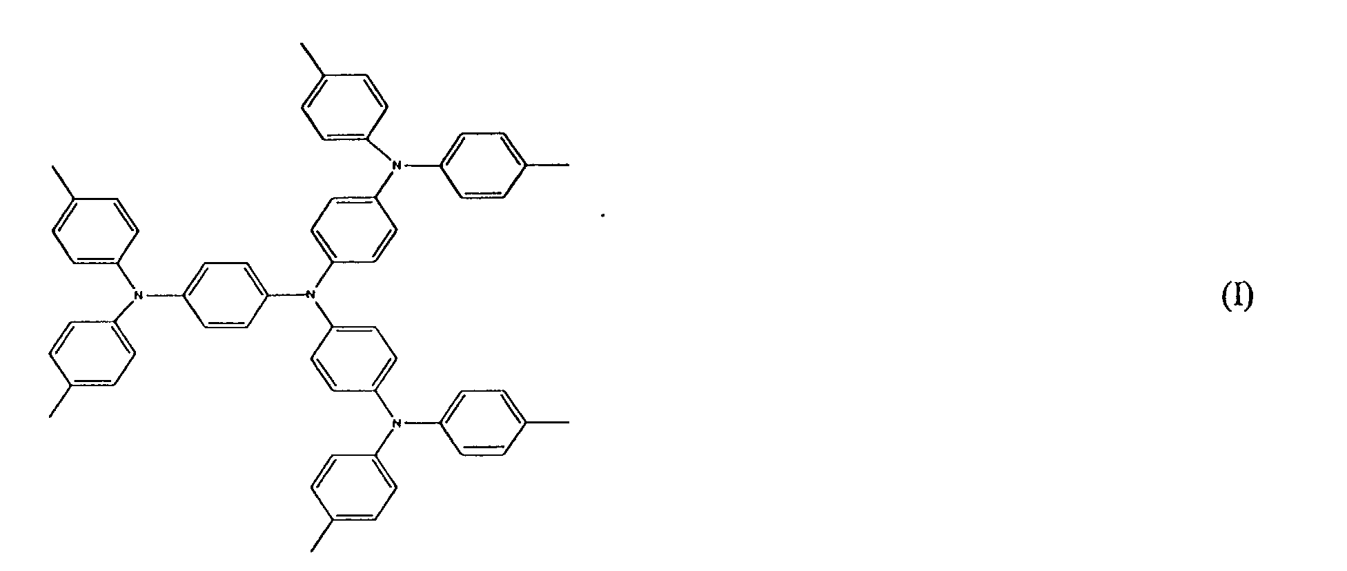
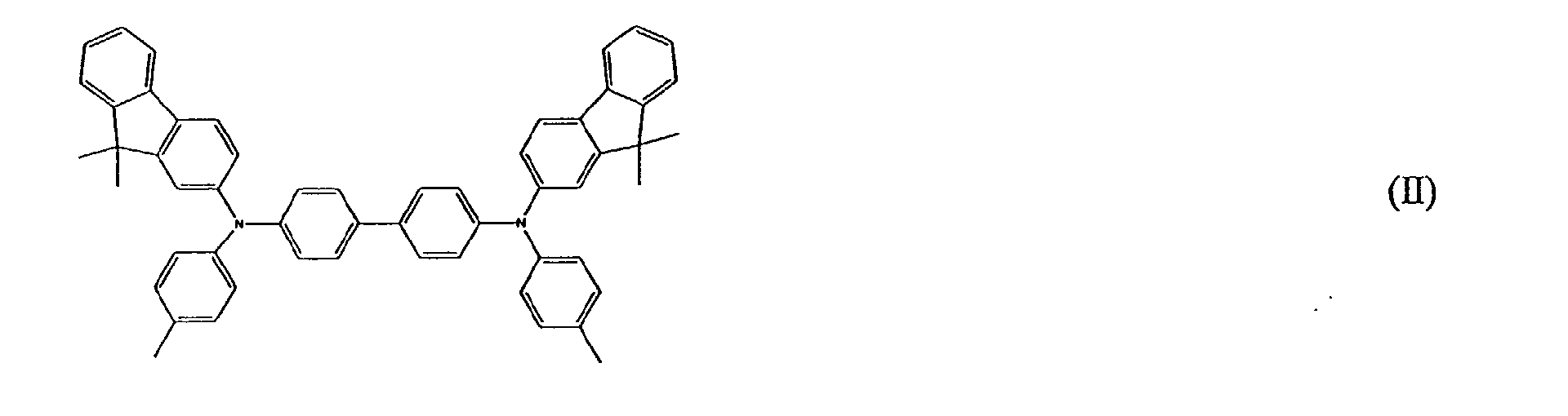


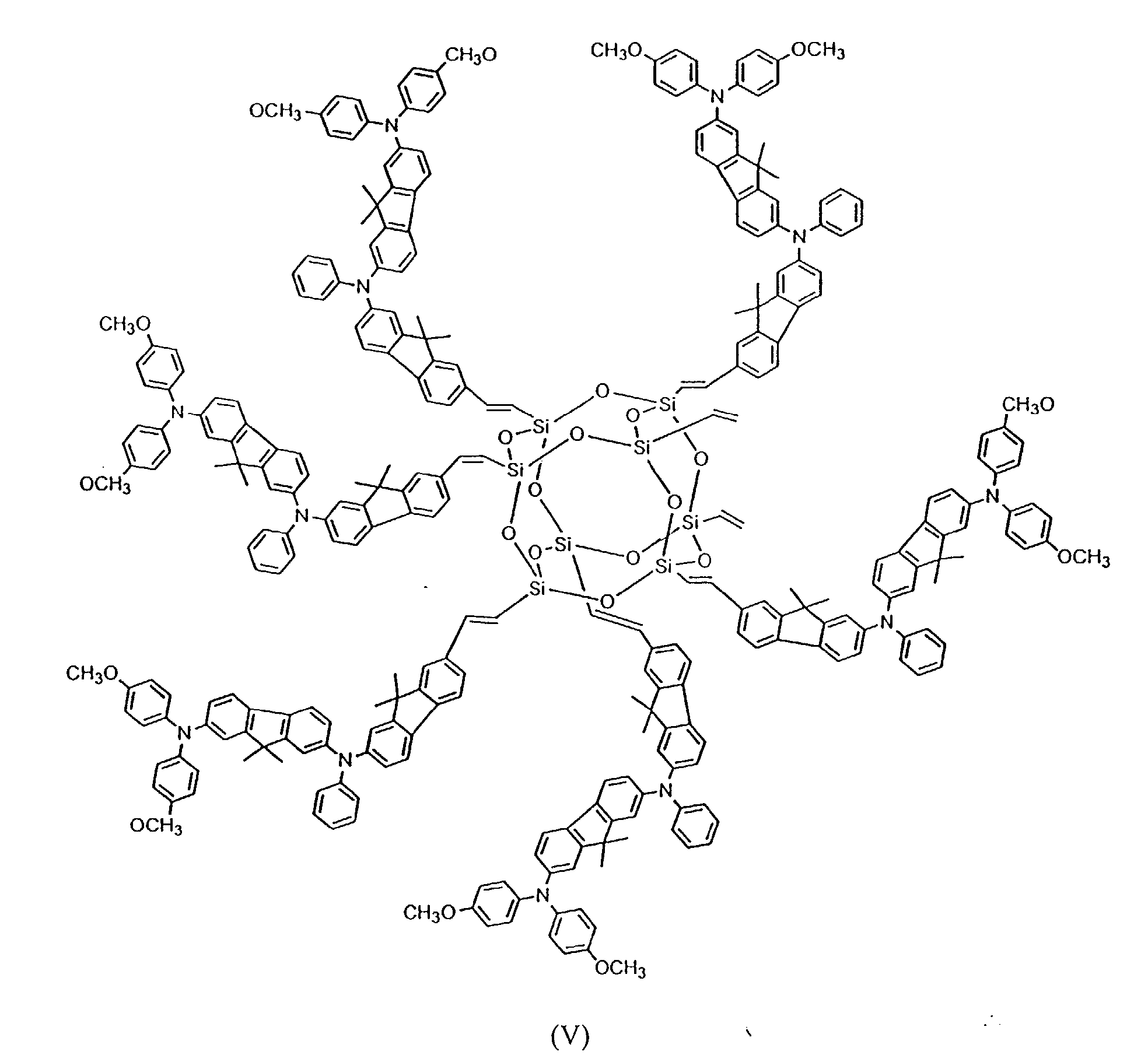
oligometallocenes. Other suitable charge transport compounds which may be oxidized to form the thin-layer oxidized charge transport materials of the invention can be selected from those disclosed in the aforementioned U.S. Patent No. 5,853,906.
Claims (16)
- An oxidized charge transport material formed substantially without a polymeric binder, having hole transport capability in an organic light emitting device, comprising
a charge transport compound including more than two triarylamine groups, or including at least one triarylamine group and at least one fluorene group, and
an oxidant complexed with said charge transport compound, wherein
a portion of said charge transport compound is not complexed with said oxidant. - The oxidized charge transport material of claim 1, wherein said oxidant has formula MmXn -, where
M is a metal selected from the group consisting of As, Sb, Au, Bi, and P,
X is a halogen selected from the group consisting of F, Cl and Br, and
m and n are integers consistent with the valence states of said metal and halogen. - The oxidized charge transport material of claim 2, wherein said oxidant is present in an amount of about 0.2 to about 20 percent by weight of said charge transport material.
- The oxidized charge transport material of claim 3, wherein said oxidant is SbF6 -, AuCl4 -, or AsF6 -.
- The oxidized charge transport material of claim 1, wherein the charge transport compound is
 or
or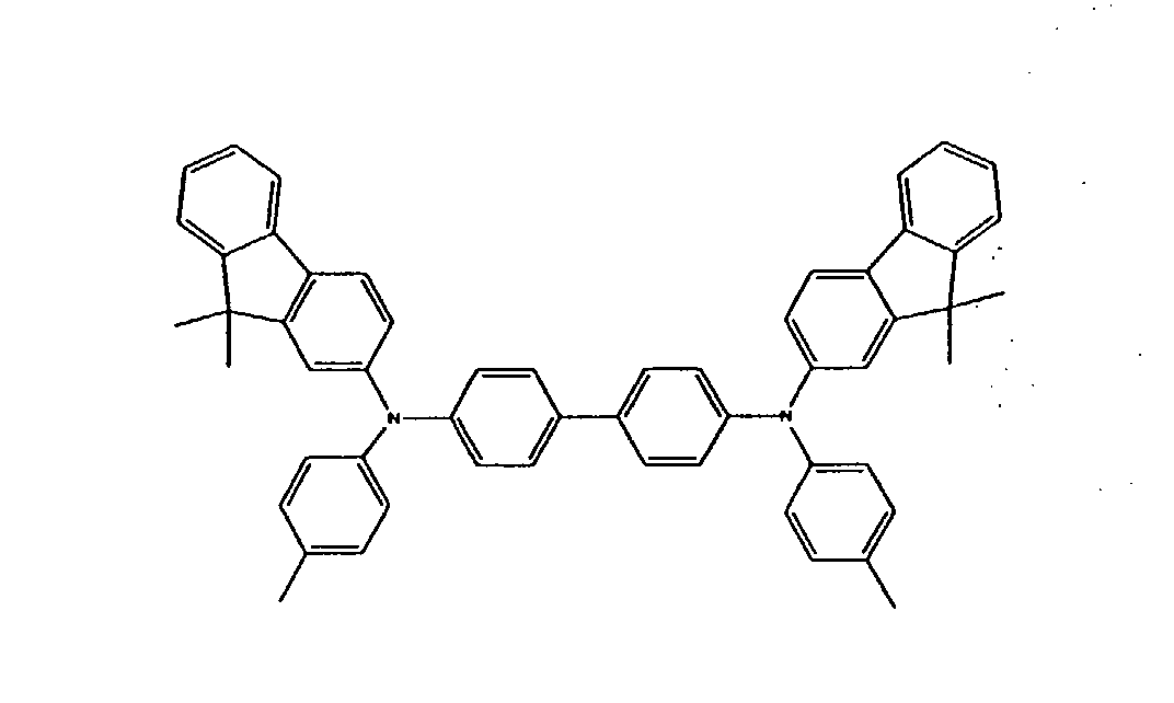

- The oxidized charge transport material of claim 1, wherein the charge transport compound comprises a polyhedral silsesquioxane core bonded to 2 to 8 aromatic amine groups.
- The oxidized charge transport material of claim 1, wherein the charge transport compound has the following formula IV or V:

- The charge transport material of claim 1 formed into a thin film of 100 Angstroms to 2000 Angstroms by solvent processing without using a polymeric binder, and having hole transport properties.
- A charge transport material capable of being formed into uniform thin film having hole injection capability in an organic light emitting device, comprising a charge transport compound selected from the group consisting of oligoarylamines, oligothiophenes, tetraselenotetracenes, mono- and oligo-tetrathiafulvalenes, oligo-tetraselenafulvalenes and oligo-metallocenes oxidized with a Lewis acid.
- An organic light emitting device comprising an anode, a cathode and an emissive layer between the anode and the cathode, and between the anode and the emissive layer, a hole injection layer formed without a polymeric binder and comprising a charge transport compound including more than two triarylamine groups, or including at least one triarylamine group and at least one fluorene group, complexed with an oxidant, wherein a portion of said charge transport compound is not complexed with said oxidant.
- The organic light emitting device of claim 10, wherein said hole injection layer is spin coated to a thickness of about 100 Angstroms to 2,000 Angstroms.
- The organic light emitting device of claim 10, wherein said hole injection layer is a thin film consisting essentially of at least one charge transport compound partly complexed with an oxidant having formula MmXn -, where
M is a metal selected from the group consisting of As, Sb, Au, Bi, and P,
X is a halogen selected from the group consisting of F, Cl and Br, and
m and n are integers consistent with the valence states of said metal and halogen. - The organic light emitting device of claim 12, wherein said hole injection layer contains said oxidant present in an amount between about 0.2 percent by weight and about 20 percent by weight of said hole injection layer.
- The organic light emitting device of claim 10 wherein the charge transport compound in the hole injection layer is
 or
or

- The organic light emitting device of claim 10 wherein the charge transport compound in the hole injection layer is:or


- The organic light emitting device of claim 10, further comprising at least one layer selected from the group consisting of electron transport layers, buffer layers, charge blocking layers, electron transport/emissive layers, and hole transport/emissive layers.
Applications Claiming Priority (2)
| Application Number | Priority Date | Filing Date | Title |
|---|---|---|---|
| US124236 | 2002-04-18 | ||
| US10/124,236 US6830830B2 (en) | 2002-04-18 | 2002-04-18 | Semiconducting hole injection materials for organic light emitting devices |
Publications (2)
| Publication Number | Publication Date |
|---|---|
| EP1359630A2 true EP1359630A2 (en) | 2003-11-05 |
| EP1359630A3 EP1359630A3 (en) | 2007-06-27 |
Family
ID=29214561
Family Applications (1)
| Application Number | Title | Priority Date | Filing Date |
|---|---|---|---|
| EP03252295A Withdrawn EP1359630A3 (en) | 2002-04-18 | 2003-04-11 | Semiconducting hole injection materials for organic light emitting devices |
Country Status (4)
| Country | Link |
|---|---|
| US (1) | US6830830B2 (en) |
| EP (1) | EP1359630A3 (en) |
| JP (1) | JP3817528B2 (en) |
| CN (1) | CN1452442A (en) |
Cited By (9)
| Publication number | Priority date | Publication date | Assignee | Title |
|---|---|---|---|---|
| KR100657575B1 (en) | 2005-03-23 | 2006-12-14 | 동양제철화학 주식회사 | Polyfluorene conjugated polymer and electroluminescent device comprising the polymer as a light emitting material |
| WO2007084816A1 (en) * | 2006-01-13 | 2007-07-26 | Dow Corning Corporation | A small molecule organic light emitting diode formed using solvent soluble materials |
| WO2008155310A1 (en) * | 2007-06-20 | 2008-12-24 | Siemens Aktiengesellschaft | Semiconductor material and organic rectifier diode |
| WO2009006550A1 (en) * | 2007-07-05 | 2009-01-08 | Nitto Denko Corporation | Light emitting devices and compositions |
| EP1768199A4 (en) * | 2004-07-14 | 2009-01-21 | Idemitsu Kosan Co | AROMATIC AMINE DERIVATIVE AND ORGANIC ELECTROLUMINESCENT DEVICE USING THE DERIVATIVE |
| US7993747B2 (en) | 2006-05-15 | 2011-08-09 | Nitto Denko Corporation | Light emitting devices and compositions comprising lumophore-functionalized nanoparticles |
| US8217569B2 (en) | 2004-12-28 | 2012-07-10 | Semiconductor Energy Laboratory Co., Ltd. | Low drive voltage light emitting element |
| US8597803B2 (en) | 2007-11-15 | 2013-12-03 | Nitto Denko Corporation | Light emitting devices and compositions |
| US8721922B2 (en) | 2008-10-13 | 2014-05-13 | Nitto Denko Corporation | Printable light-emitting compositions |
Families Citing this family (25)
| Publication number | Priority date | Publication date | Assignee | Title |
|---|---|---|---|---|
| US7960587B2 (en) * | 2004-02-19 | 2011-06-14 | E.I. Du Pont De Nemours And Company | Compositions comprising novel compounds and electronic devices made with such compositions |
| US7365230B2 (en) * | 2004-02-20 | 2008-04-29 | E.I. Du Pont De Nemours And Company | Cross-linkable polymers and electronic devices made with such polymers |
| KR20060133056A (en) | 2004-03-31 | 2006-12-22 | 이 아이 듀폰 디 네모아 앤드 캄파니 | Triarylamine Compounds for Charge Transport Materials |
| JP2006111790A (en) * | 2004-10-18 | 2006-04-27 | Seiko Epson Corp | Conductive adhesive |
| JP4235619B2 (en) * | 2005-02-14 | 2009-03-11 | キヤノン株式会社 | Manufacturing method of organic light emitting device |
| US7888859B2 (en) * | 2005-03-02 | 2011-02-15 | Konica Minolta Holdings Inc. | Organic electroluminescence element, display device and lighting device |
| KR101156426B1 (en) * | 2005-08-25 | 2012-06-18 | 삼성모바일디스플레이주식회사 | An silsesquioxane-based compound and an organic light emitting device comprising the same |
| KR101193179B1 (en) * | 2005-08-26 | 2012-10-19 | 삼성디스플레이 주식회사 | Organosiloxane compound and organic electroluminescence device comprsing the same |
| US7915809B2 (en) * | 2005-10-07 | 2011-03-29 | Dow Corning Corporation | Electrophosphorescent organic light emitting diode formed using solvent soluble materials |
| KR101193180B1 (en) * | 2005-11-14 | 2012-10-19 | 삼성디스플레이 주식회사 | A conducting polymer composition and an electronic device employing the layer obtained from the conducting polymer composition |
| KR101243917B1 (en) * | 2005-12-19 | 2013-03-14 | 삼성디스플레이 주식회사 | A conducting polymer composition and an electrical device employing the layer obtained from the conducting polymer composition |
| KR100789147B1 (en) | 2006-11-03 | 2007-12-28 | 주식회사 효성 | Method for producing polyethylene terephthalate nanocomposite fiber with improved modulus |
| PL1986473T3 (en) * | 2007-04-03 | 2017-07-31 | Tsinghua University | Organic electroluminescent device |
| JP5472121B2 (en) | 2009-01-28 | 2014-04-16 | コニカミノルタ株式会社 | ORGANIC ELECTROLUMINESCENT ELEMENT, DISPLAY DEVICE AND LIGHTING DEVICE, AND METHOD FOR PRODUCING ORGANIC ELECTROLUMINESCENT ELEMENT |
| US8785004B2 (en) | 2009-01-30 | 2014-07-22 | Hewlett-Packard Development Company, L.P. | UV light-emissive fluorene-based copolymers |
| WO2010087841A1 (en) | 2009-01-30 | 2010-08-05 | Hewlett-Packard Development Company | Block copolymers and block copolymer nanoparticle compositions |
| JP2013508380A (en) * | 2009-10-19 | 2013-03-07 | イー・アイ・デュポン・ドウ・ヌムール・アンド・カンパニー | Triarylamine compounds for electronic applications |
| JP2013508375A (en) | 2009-10-19 | 2013-03-07 | イー・アイ・デュポン・ドウ・ヌムール・アンド・カンパニー | Triarylamine compounds for electronic applications |
| KR20110112641A (en) * | 2010-04-07 | 2011-10-13 | 한국과학기술연구원 | Polysilsesquioxane of ladder structure having photoactive group as side chain and its preparation method |
| JPWO2013031662A1 (en) * | 2011-08-26 | 2015-03-23 | コニカミノルタ株式会社 | Organic electroluminescence element, lighting device and display device |
| GB201309668D0 (en) | 2013-05-30 | 2013-07-17 | Isis Innovation | Organic semiconductor doping process |
| US10090477B2 (en) * | 2014-05-23 | 2018-10-02 | Nissan Chemical Industries, Ltd. | Charge-transporting varnish |
| US10564142B2 (en) | 2017-09-29 | 2020-02-18 | Saudi Arabian Oil Company | Quantifying organic and inorganic sulfur components |
| CN108365001A (en) * | 2018-04-16 | 2018-08-03 | 江苏集萃有机光电技术研究所有限公司 | A kind of ITO substrates and preparation method thereof |
| CN118076183A (en) * | 2022-11-22 | 2024-05-24 | Tcl科技集团股份有限公司 | Method for preparing light-emitting device, light-emitting device and electronic device |
Family Cites Families (23)
| Publication number | Priority date | Publication date | Assignee | Title |
|---|---|---|---|---|
| US4055091A (en) | 1972-08-31 | 1977-10-25 | Ker-Train Systems N.V. | Variable output transmission |
| US4005091A (en) | 1974-12-20 | 1977-01-25 | E. I. Du Pont De Nemours And Company | Substituted trimethylene cyclopropanes, salts thereof, intermediates and methods of making the same |
| US3963769A (en) | 1974-12-20 | 1976-06-15 | E. I. Du Pont De Nemours And Company | Substituted trimethylene cyclopropanes, salts thereof, intermediates and methods of making the same |
| US4338222A (en) | 1980-04-11 | 1982-07-06 | Xerox Corporation | Semiconductive organic compositions |
| JP3016896B2 (en) * | 1991-04-08 | 2000-03-06 | パイオニア株式会社 | Organic electroluminescence device |
| US5549851A (en) | 1994-01-25 | 1996-08-27 | Shin-Etsu Chemical Co., Ltd. | Conductive polymer composition |
| US5834080A (en) | 1994-10-18 | 1998-11-10 | Xerox Corporation | Controllably conductive polymer compositions for development systems |
| US5587224A (en) | 1995-03-27 | 1996-12-24 | Xerox Corporation | Developing apparatus including a coated developer roller |
| US5719467A (en) * | 1995-07-27 | 1998-02-17 | Hewlett-Packard Company | Organic electroluminescent device |
| JP3871396B2 (en) * | 1997-04-03 | 2007-01-24 | 靖彦 城田 | Organic EL device |
| JP3508984B2 (en) * | 1997-05-19 | 2004-03-22 | キヤノン株式会社 | Organic compound and light emitting device using the organic compound |
| US5853906A (en) * | 1997-10-14 | 1998-12-29 | Xerox Corporation | Conductive polymer compositions and processes thereof |
| US5968674A (en) | 1997-10-14 | 1999-10-19 | Xerox Corporation | Conductive polymer coatings and processes thereof |
| JPH11251067A (en) * | 1998-03-02 | 1999-09-17 | Junji Kido | Organic electroluminescent device |
| US5976418A (en) | 1998-11-05 | 1999-11-02 | Xerox Corporation | Conducting compositions |
| US6107439A (en) | 1998-12-22 | 2000-08-22 | Xerox Corporation | Cross linked conducting compositions |
| JP2000196140A (en) * | 1998-12-28 | 2000-07-14 | Sharp Corp | Organic electroluminescent device and manufacturing method thereof |
| TW474114B (en) * | 1999-09-29 | 2002-01-21 | Junji Kido | Organic electroluminescent device, organic electroluminescent device assembly and method of controlling the emission spectrum in the device |
| US6139999A (en) | 1999-10-28 | 2000-10-31 | Xerox Corporation | Imaging member with partially conductive overcoating |
| US6197462B1 (en) | 1999-11-29 | 2001-03-06 | Xerox Corporation | Cross-linked polyamide anticurl back coating for electrostatographic imaging members |
| JP4144192B2 (en) * | 2000-05-29 | 2008-09-03 | 三菱化学株式会社 | Method for manufacturing organic electroluminescent device |
| US6517958B1 (en) * | 2000-07-14 | 2003-02-11 | Canon Kabushiki Kaisha | Organic-inorganic hybrid light emitting devices (HLED) |
| JP3933591B2 (en) * | 2002-03-26 | 2007-06-20 | 淳二 城戸 | Organic electroluminescent device |
-
2002
- 2002-04-18 US US10/124,236 patent/US6830830B2/en not_active Expired - Fee Related
-
2003
- 2003-04-11 EP EP03252295A patent/EP1359630A3/en not_active Withdrawn
- 2003-04-17 CN CN03123115A patent/CN1452442A/en active Pending
- 2003-04-18 JP JP2003114192A patent/JP3817528B2/en not_active Expired - Fee Related
Cited By (11)
| Publication number | Priority date | Publication date | Assignee | Title |
|---|---|---|---|---|
| EP1768199A4 (en) * | 2004-07-14 | 2009-01-21 | Idemitsu Kosan Co | AROMATIC AMINE DERIVATIVE AND ORGANIC ELECTROLUMINESCENT DEVICE USING THE DERIVATIVE |
| US8217569B2 (en) | 2004-12-28 | 2012-07-10 | Semiconductor Energy Laboratory Co., Ltd. | Low drive voltage light emitting element |
| US8519615B2 (en) | 2004-12-28 | 2013-08-27 | Semiconductor Energy Laboratory Co., Ltd. | Low drive voltage light emitting element |
| KR100657575B1 (en) | 2005-03-23 | 2006-12-14 | 동양제철화학 주식회사 | Polyfluorene conjugated polymer and electroluminescent device comprising the polymer as a light emitting material |
| WO2007084816A1 (en) * | 2006-01-13 | 2007-07-26 | Dow Corning Corporation | A small molecule organic light emitting diode formed using solvent soluble materials |
| US7993747B2 (en) | 2006-05-15 | 2011-08-09 | Nitto Denko Corporation | Light emitting devices and compositions comprising lumophore-functionalized nanoparticles |
| WO2008155310A1 (en) * | 2007-06-20 | 2008-12-24 | Siemens Aktiengesellschaft | Semiconductor material and organic rectifier diode |
| WO2009006550A1 (en) * | 2007-07-05 | 2009-01-08 | Nitto Denko Corporation | Light emitting devices and compositions |
| US8609258B2 (en) | 2007-07-05 | 2013-12-17 | Nitto Denko Corporation | Light emitting devices and compositions |
| US8597803B2 (en) | 2007-11-15 | 2013-12-03 | Nitto Denko Corporation | Light emitting devices and compositions |
| US8721922B2 (en) | 2008-10-13 | 2014-05-13 | Nitto Denko Corporation | Printable light-emitting compositions |
Also Published As
| Publication number | Publication date |
|---|---|
| CN1452442A (en) | 2003-10-29 |
| US20030207152A1 (en) | 2003-11-06 |
| JP2004006321A (en) | 2004-01-08 |
| US6830830B2 (en) | 2004-12-14 |
| EP1359630A3 (en) | 2007-06-27 |
| JP3817528B2 (en) | 2006-09-06 |
Similar Documents
| Publication | Publication Date | Title |
|---|---|---|
| US6830830B2 (en) | Semiconducting hole injection materials for organic light emitting devices | |
| CN102484210B (en) | Containing the nano particle of transistion metal compound and manufacture method thereof, hole injection/transport layer ink and device and the manufacture method thereof with hole injection/transport layer | |
| JP4957863B2 (en) | Transition metal-containing nanoparticles for forming a hole injecting and transporting layer and method for producing the same | |
| JP5760334B2 (en) | Organic electronic device and manufacturing method thereof | |
| CN1190322A (en) | organic electroluminescent element | |
| JP2001223084A (en) | Organic electroluminescent device | |
| EP1638372B1 (en) | Charge-transporting varnish | |
| JP4140323B2 (en) | Organic electroluminescence device | |
| KR20110000732A (en) | Interlayer forming coating liquid, manufacturing method of organic electroluminescent element, and organic electroluminescent element | |
| JP4314771B2 (en) | Organic electroluminescence device | |
| KR100858458B1 (en) | Organic electroluminescent device | |
| JPH05271652A (en) | Organic thin-film el element | |
| US20060267487A1 (en) | Method for producing polymer organic electronic material, polymer organic electronic material, and organic electroluminescent device | |
| EP1175130B1 (en) | Electroluminescent element | |
| EP1186067B1 (en) | Conducting polymers | |
| JP2005506665A (en) | Electrophosphorescent assembly containing conducting polymer | |
| JP4449282B2 (en) | Organic electroluminescence device | |
| JP2007194338A5 (en) | ||
| JP2007194338A (en) | Organic electroluminescent device and manufacturing method thereof | |
| KR102749889B1 (en) | Emitting material, coating composition, organic light emitting device and manufacturing method thereof | |
| JP2007043132A (en) | Organic electroluminescence element using conductive particulate | |
| JP4258192B2 (en) | Organic electroluminescence device | |
| KR100406463B1 (en) | Organic light-emitting device using composition of bis(10-hydroxybenzoquinolinato)beryllium and bis(2-methyl-8-hydroxyquinolinato) beryllium as light-emitting material | |
| JP4779325B2 (en) | Organic electroluminescence device | |
| JP4815830B2 (en) | Organic electroluminescent device, organic electroluminescent device manufacturing method and image display medium |
Legal Events
| Date | Code | Title | Description |
|---|---|---|---|
| PUAI | Public reference made under article 153(3) epc to a published international application that has entered the european phase |
Free format text: ORIGINAL CODE: 0009012 |
|
| AK | Designated contracting states |
Kind code of ref document: A2 Designated state(s): AT BE BG CH CY CZ DE DK EE ES FI FR GB GR HU IE IT LI LU MC NL PT RO SE SI SK TR |
|
| AX | Request for extension of the european patent |
Extension state: AL LT LV MK |
|
| PUAL | Search report despatched |
Free format text: ORIGINAL CODE: 0009013 |
|
| AK | Designated contracting states |
Kind code of ref document: A3 Designated state(s): AT BE BG CH CY CZ DE DK EE ES FI FR GB GR HU IE IT LI LU MC NL PT RO SE SI SK TR |
|
| AX | Request for extension of the european patent |
Extension state: AL LT LV MK |
|
| 17P | Request for examination filed |
Effective date: 20071227 |
|
| AKX | Designation fees paid |
Designated state(s): DE FR GB IT |
|
| STAA | Information on the status of an ep patent application or granted ep patent |
Free format text: STATUS: THE APPLICATION HAS BEEN WITHDRAWN |
|
| 17Q | First examination report despatched |
Effective date: 20080215 |
|
| 18W | Application withdrawn |
Effective date: 20080304 |