EP1359576A2 - Optical recording medium and method for optically recording data on the same - Google Patents
Optical recording medium and method for optically recording data on the same Download PDFInfo
- Publication number
- EP1359576A2 EP1359576A2 EP03009702A EP03009702A EP1359576A2 EP 1359576 A2 EP1359576 A2 EP 1359576A2 EP 03009702 A EP03009702 A EP 03009702A EP 03009702 A EP03009702 A EP 03009702A EP 1359576 A2 EP1359576 A2 EP 1359576A2
- Authority
- EP
- European Patent Office
- Prior art keywords
- recording layer
- layer
- recording
- recording medium
- optical recording
- Prior art date
- Legal status (The legal status is an assumption and is not a legal conclusion. Google has not performed a legal analysis and makes no representation as to the accuracy of the status listed.)
- Withdrawn
Links
Images



Classifications
-
- G—PHYSICS
- G11—INFORMATION STORAGE
- G11B—INFORMATION STORAGE BASED ON RELATIVE MOVEMENT BETWEEN RECORD CARRIER AND TRANSDUCER
- G11B7/00—Recording or reproducing by optical means, e.g. recording using a thermal beam of optical radiation by modifying optical properties or the physical structure, reproducing using an optical beam at lower power by sensing optical properties; Record carriers therefor
- G11B7/24—Record carriers characterised by shape, structure or physical properties, or by the selection of the material
- G11B7/2403—Layers; Shape, structure or physical properties thereof
- G11B7/24035—Recording layers
-
- G—PHYSICS
- G11—INFORMATION STORAGE
- G11B—INFORMATION STORAGE BASED ON RELATIVE MOVEMENT BETWEEN RECORD CARRIER AND TRANSDUCER
- G11B7/00—Recording or reproducing by optical means, e.g. recording using a thermal beam of optical radiation by modifying optical properties or the physical structure, reproducing using an optical beam at lower power by sensing optical properties; Record carriers therefor
- G11B7/004—Recording, reproducing or erasing methods; Read, write or erase circuits therefor
- G11B7/0045—Recording
-
- G—PHYSICS
- G11—INFORMATION STORAGE
- G11B—INFORMATION STORAGE BASED ON RELATIVE MOVEMENT BETWEEN RECORD CARRIER AND TRANSDUCER
- G11B7/00—Recording or reproducing by optical means, e.g. recording using a thermal beam of optical radiation by modifying optical properties or the physical structure, reproducing using an optical beam at lower power by sensing optical properties; Record carriers therefor
- G11B7/24—Record carriers characterised by shape, structure or physical properties, or by the selection of the material
- G11B7/2403—Layers; Shape, structure or physical properties thereof
- G11B7/24035—Recording layers
- G11B7/24038—Multiple laminated recording layers
-
- G—PHYSICS
- G11—INFORMATION STORAGE
- G11B—INFORMATION STORAGE BASED ON RELATIVE MOVEMENT BETWEEN RECORD CARRIER AND TRANSDUCER
- G11B7/00—Recording or reproducing by optical means, e.g. recording using a thermal beam of optical radiation by modifying optical properties or the physical structure, reproducing using an optical beam at lower power by sensing optical properties; Record carriers therefor
- G11B7/24—Record carriers characterised by shape, structure or physical properties, or by the selection of the material
- G11B7/241—Record carriers characterised by shape, structure or physical properties, or by the selection of the material characterised by the selection of the material
- G11B7/242—Record carriers characterised by shape, structure or physical properties, or by the selection of the material characterised by the selection of the material of recording layers
- G11B7/243—Record carriers characterised by shape, structure or physical properties, or by the selection of the material characterised by the selection of the material of recording layers comprising inorganic materials only, e.g. ablative layers
-
- G—PHYSICS
- G11—INFORMATION STORAGE
- G11B—INFORMATION STORAGE BASED ON RELATIVE MOVEMENT BETWEEN RECORD CARRIER AND TRANSDUCER
- G11B7/00—Recording or reproducing by optical means, e.g. recording using a thermal beam of optical radiation by modifying optical properties or the physical structure, reproducing using an optical beam at lower power by sensing optical properties; Record carriers therefor
- G11B7/24—Record carriers characterised by shape, structure or physical properties, or by the selection of the material
- G11B7/241—Record carriers characterised by shape, structure or physical properties, or by the selection of the material characterised by the selection of the material
- G11B7/242—Record carriers characterised by shape, structure or physical properties, or by the selection of the material characterised by the selection of the material of recording layers
- G11B7/243—Record carriers characterised by shape, structure or physical properties, or by the selection of the material characterised by the selection of the material of recording layers comprising inorganic materials only, e.g. ablative layers
- G11B2007/24302—Metals or metalloids
- G11B2007/24304—Metals or metalloids group 2 or 12 elements (e.g. Be, Ca, Mg, Zn, Cd)
-
- G—PHYSICS
- G11—INFORMATION STORAGE
- G11B—INFORMATION STORAGE BASED ON RELATIVE MOVEMENT BETWEEN RECORD CARRIER AND TRANSDUCER
- G11B7/00—Recording or reproducing by optical means, e.g. recording using a thermal beam of optical radiation by modifying optical properties or the physical structure, reproducing using an optical beam at lower power by sensing optical properties; Record carriers therefor
- G11B7/24—Record carriers characterised by shape, structure or physical properties, or by the selection of the material
- G11B7/241—Record carriers characterised by shape, structure or physical properties, or by the selection of the material characterised by the selection of the material
- G11B7/242—Record carriers characterised by shape, structure or physical properties, or by the selection of the material characterised by the selection of the material of recording layers
- G11B7/243—Record carriers characterised by shape, structure or physical properties, or by the selection of the material characterised by the selection of the material of recording layers comprising inorganic materials only, e.g. ablative layers
- G11B2007/24302—Metals or metalloids
- G11B2007/24308—Metals or metalloids transition metal elements of group 11 (Cu, Ag, Au)
-
- G—PHYSICS
- G11—INFORMATION STORAGE
- G11B—INFORMATION STORAGE BASED ON RELATIVE MOVEMENT BETWEEN RECORD CARRIER AND TRANSDUCER
- G11B7/00—Recording or reproducing by optical means, e.g. recording using a thermal beam of optical radiation by modifying optical properties or the physical structure, reproducing using an optical beam at lower power by sensing optical properties; Record carriers therefor
- G11B7/24—Record carriers characterised by shape, structure or physical properties, or by the selection of the material
- G11B7/241—Record carriers characterised by shape, structure or physical properties, or by the selection of the material characterised by the selection of the material
- G11B7/242—Record carriers characterised by shape, structure or physical properties, or by the selection of the material characterised by the selection of the material of recording layers
- G11B7/243—Record carriers characterised by shape, structure or physical properties, or by the selection of the material characterised by the selection of the material of recording layers comprising inorganic materials only, e.g. ablative layers
- G11B2007/24302—Metals or metalloids
- G11B2007/2431—Metals or metalloids group 13 elements (B, Al, Ga, In)
-
- G—PHYSICS
- G11—INFORMATION STORAGE
- G11B—INFORMATION STORAGE BASED ON RELATIVE MOVEMENT BETWEEN RECORD CARRIER AND TRANSDUCER
- G11B7/00—Recording or reproducing by optical means, e.g. recording using a thermal beam of optical radiation by modifying optical properties or the physical structure, reproducing using an optical beam at lower power by sensing optical properties; Record carriers therefor
- G11B7/24—Record carriers characterised by shape, structure or physical properties, or by the selection of the material
- G11B7/241—Record carriers characterised by shape, structure or physical properties, or by the selection of the material characterised by the selection of the material
- G11B7/242—Record carriers characterised by shape, structure or physical properties, or by the selection of the material characterised by the selection of the material of recording layers
- G11B7/243—Record carriers characterised by shape, structure or physical properties, or by the selection of the material characterised by the selection of the material of recording layers comprising inorganic materials only, e.g. ablative layers
- G11B2007/24302—Metals or metalloids
- G11B2007/24312—Metals or metalloids group 14 elements (e.g. Si, Ge, Sn)
-
- G—PHYSICS
- G11—INFORMATION STORAGE
- G11B—INFORMATION STORAGE BASED ON RELATIVE MOVEMENT BETWEEN RECORD CARRIER AND TRANSDUCER
- G11B7/00—Recording or reproducing by optical means, e.g. recording using a thermal beam of optical radiation by modifying optical properties or the physical structure, reproducing using an optical beam at lower power by sensing optical properties; Record carriers therefor
- G11B7/24—Record carriers characterised by shape, structure or physical properties, or by the selection of the material
- G11B7/241—Record carriers characterised by shape, structure or physical properties, or by the selection of the material characterised by the selection of the material
- G11B7/242—Record carriers characterised by shape, structure or physical properties, or by the selection of the material characterised by the selection of the material of recording layers
- G11B7/243—Record carriers characterised by shape, structure or physical properties, or by the selection of the material characterised by the selection of the material of recording layers comprising inorganic materials only, e.g. ablative layers
- G11B2007/24318—Non-metallic elements
- G11B2007/24328—Carbon
-
- G—PHYSICS
- G11—INFORMATION STORAGE
- G11B—INFORMATION STORAGE BASED ON RELATIVE MOVEMENT BETWEEN RECORD CARRIER AND TRANSDUCER
- G11B7/00—Recording or reproducing by optical means, e.g. recording using a thermal beam of optical radiation by modifying optical properties or the physical structure, reproducing using an optical beam at lower power by sensing optical properties; Record carriers therefor
- G11B7/24—Record carriers characterised by shape, structure or physical properties, or by the selection of the material
- G11B7/241—Record carriers characterised by shape, structure or physical properties, or by the selection of the material characterised by the selection of the material
- G11B7/252—Record carriers characterised by shape, structure or physical properties, or by the selection of the material characterised by the selection of the material of layers other than recording layers
- G11B7/258—Record carriers characterised by shape, structure or physical properties, or by the selection of the material characterised by the selection of the material of layers other than recording layers of reflective layers
Definitions
- the present invention relates to an optical recording medium and a method for optically recording data in the optical recording medium and, particularly, to an optical recording medium constituted so as to record data therein and reproduce data therefrom by projecting a laser beam onto the side opposite from a substrate, which includes two or more recording layers and is capable of decreasing noise level and improving C/N ratio of a reproduced signal, and a method for optically recording data in the same.
- optical recording media such as the CD, DVD and the like have been widely used as recording media for recording digital data.
- These optical recording media can be roughly classified into optical recording media such as the CD-ROM and the DVD-ROM that do not enable writing and rewriting of data (ROM type optical recording media), optical recording media such as the CD-R and DVD-R that enable writing but not rewriting of data (write-once type optical recording media), and optical recording media such as the CD-RW and DVD-RW that enable rewriting of data (data rewritable type optical recording media).
- phase change material is generally used as the material of the recording layer and data are recorded utilizing changes in an optical characteristic caused by phase change of the phase change material.
- an organic dye such as a cyanine dye, phthalocyanine dye or azo dye is generally used as the material of the recording layer and data are recorded utilizing changes in an optical characteristic caused by chemical change of the organic dye, which change may be accompanied by physical deformation.
- an optical recording material formed by laminating two recording layers is known as an example of an optical recording medium whose recording layer is formed of a material other than an organic dye.
- Equation (1) the permitted tilt error of the optical axis of the laser beam to the optical recording medium, namely, the tilt margin T , has to be greatly decreased.
- Equation (1) ⁇ is the wavelength of the laser beam used for recording and reproducing data and d is the thickness of the light transmission layer through which the laser beam transmits.
- the tilt margin T decreases as the numerical aperture of the objective lens increases and increases as the thickness of the light transmission layer decreases. Therefore, decrease of the tilt margin T can be effectively prevented by making the thickness of the light transmission layer thinner.
- Equation (2) a wave aberration coefficient W representing coma is defined by Equation (2).
- W d • (n 2 - 1)• n 2 • sin ⁇ • cos ⁇ • ( NA ) 3 2 ⁇ ( n 2 - sin 2 ⁇ ) 5 2
- Equation (2) n is the refractive index of the light transmission layer and ⁇ is the tilt of the optical axis of the laser beam.
- the thickness of the light transmission layer of the next-generation type optical recording medium should be reduced as far as about 100 ⁇ m in order to ensure sufficient tilt margin and suppress coma.
- the light transmission layer be constituted as a thin resin layer formed by spin coating or the like on a recording layer or other such layer formed on a substrate.
- layers are sequentially formed from the side of the light incidence surface in a conventional optical recording medium, they are sequentially formed from the side opposite from the light incidence surface in a next-generation optical recording medium.
- the inventors of the present invention vigorously pursued a study for accomplishing the above objects and, as a result, made the surprising discovery that when a laser beam is used to record data in an optical recording medium composed of a first recording layer containing an element selected from the group consisting of Si, Ge, C and Al as a primary component and a second recording layer containing Zn as a primary component and formed in the vicinity of the first recording layer so that the total thickness of the first recording layer and the second recording layer is equal to or thinner than 30 nm, a mixed region including both the primary component element of the first recording layer and the primary component element of the second recording layer is formed to markedly change the region's reflection coefficient and enable data to be recorded with high sensitivity.
- the noise level of a reproduced signal can be decreased to improve C/N ratio by utilizing the large difference in reflection coefficient between the mixed region including the primary component element of the first recording layer and the primary component element of the second recording layer, and the other regions.
- an optical recording medium comprising a substrate, a first recording layer formed on the substrate and containing an element selected from the group consisting of Si, Ge, C and Al as a primary component, and a second recording layer located in the vicinity of the first recording layer and containing Zn as a primary component, the optical recording medium being constituted to be irradiated by a laser beam projected onto the side opposite from the substrate and the total thickness of the first recording layer and the second recording layer being equal to or thinner than 30 nm.
- a method for optically recording data comprising a step of projecting a laser beam of predetermined power onto the side opposite from a substrate of an optical recording medium comprising a substrate, a first recording layer formed on the substrate and containing an element selected from the group consisting of Si, Ge, C and Al as a primary component, and a second recording layer located in the vicinity of the first recording layer and containing Zn as a primary component, the optical recording medium being constituted to be irradiated by a laser beam projected onto the side opposite from the substrate and the total thickness of the first recording layer and the second recording layer being equal to or thinner than 30 nm.
- the statement that the first recording layer contains a certain element as a primary component means that the content of the element is maximum among the elements contained in the first recording layer
- the statement that the second recording layer contains Zn as a primary component means that the content of Zn is maximum among the elements contained in the second recording layer
- the second recording layer it is not absolutely necessary for the second recording layer to be in contact with the first recording layer and it is sufficient for the second recording layer to be so located in the vicinity of the first recording layer as to enable formation of a mixed region including the primary component element of the first recording layer and the primary component element of the second recording layer when the region is irradiated with a laser beam.
- one or more other layers such as a dielectric layer may be interposed between the first recording layer and the second recording layer.
- the second recording layer it is preferable to form the second recording layer so as to be in contact with the first recording layer.
- the optical recording medium may include one or more recording layers containing an element selected from the group consisting of Si, Ge, C and Al as a primary component or one or more recording layers containing Zn as a primary element, in addition to the first recording layer and the second recording layer.
- the first recording layer preferably contains an element selected from the group consisting of Si, Ge and C as a primary component.
- the first recording layer contains Si as a primary component.
- the reflection coefficient that the region thus formed by mixing the primary component elements of the first and second recording layers exhibits with respect to a laser beam for reproducing data and the reflection coefficient that other regions exhibit with respect to the laser beam for reproducing data are considerably different and, therefore, recorded data can be reproduced with high sensitivity by utilizing such large difference in the reflection coefficients,
- an optical recording medium constituted to be irradiated by a laser beam projected from the side of a substrate formed by injection molding to have excellent surface smoothness
- a first recording layer and a second recording layer are sequentially formed on the substrate by a gas phase growth process
- the first recording layer which is contact with the smooth surface of the substrate and on which the laser beam impinges, will also have excellent surface smoothness.
- the noise level of a reproduced signal is therefore not increased.
- an optical recording medium including a first recording layer and a second recording layer sequentially formed on a substrate by a gas phase growth process and constituted to be irradiated by a laser beam projected onto the side opposite from the substrate
- the laser beam impinges on the surface of the second recording layer, which has poor surface smoothness because it is formed by a gas phase growth process on the first recording layer that is formed on the substrate by a gas phase growth process and has poor surface smoothness.
- next-generation optical recording medium constituted so that data are recorded therein and reproduced therefrom using a laser beam having a short wavelength and an objective lens having a large numerical aperture
- the noise level of a reproduced signal and, therefore, the C/N ratio are greatly affected by the smoothness of the surface of the second recording layer. Therefore, when the smoothness of the surface of the second recording layer is poor, the noise level of a reproduced signal is greatly increased and the C/N ratio is markedly decreased.
- the smoothness of the surface of the second recording layer on which the laser beam impinges can be improved and, therefore, it is possible to effectively prevent the noise level of the reproduced signal from being increased, thereby preventing the C/N ratio from being lowered.
- the first recording layer and the second recording layer are preferably formed so that a total thickness thereof is 2 nm to 30 nm, more preferably, 2 nm to 24 nm, most preferably, 2 nm to 12 nm.
- the first recording layer may contain an element selected from the group consisting of Sn, Au, Cu, B, Mg, Ti, Mn, Fe, Ga, Zr, Ag and Pt as a primary component.
- At least one kind of an element selected from the group consisting of Mg, Cu and Al is added to the second recording layer.
- at least one kind of an element selected from the group consisting of Mg, Cu and Al is added to the second recording layer, it is possible to further decrease a noise level in a reproduced signal and improve a long term storage reliability.
- At least one element selected from the group consisting of Au, Ti, Si, Sn, Ge, P, Cr and Pt may be added to the second recording layer instead of at least one element selected from the group consisting of Mg, Cu and Al or in addition to at least one element selected from the group consisting of Mg, Cu and Al.
- an optical recording medium further comprises a light transmission layer provided on a side opposite to the substrate with respect to the first recording layer and the second recording layer, a first dielectric layer provided between the light transmission layer and the first recording layer and the second recording layer, and a second dielectric layer provided between the first recording layer and the second recording layer and the substrate.
- an optical recording medium further comprises a reflective layer provided between the substrate and the second dielectric layer.
- the method for optically recording data includes a step of projecting a laser beam having a wavelength of 450 nm or shorter onto the optical recording medium, thereby recording data in the first recording layer and the second recording layer.
- the method for optically recording data includes the steps of employing an objective lens and a laser beam whose numerical aperture NA and wavelength ⁇ satisfy ⁇ /NA ⁇ 640 nm, and projecting the laser beam onto the optical recording medium via the objective lens, thereby recording data in the first recording layer and the second recording layer.
- the recording density of data can be markedly improved.
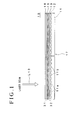
- Figure 1 is a schematic cross-sectional view showing the structure of an optical recording medium that is a preferred embodiment of the present invention.
- an optical recording medium 10 is constituted as a write-once type optical recording medium and includes a substrate 11, a reflective layer 12 formed on the surface of the substrate 11, a second dielectric layer 13 formed on the surface of the reflective layer 12, a second recording layer 32 formed on the surface of the second dielectric layer 13, a first recording layer 31 formed on the surface of the second recording layer 32, a first dielectric layer 15 formed on the surface of the first recording layer 31 and a light transmission layer 16 formed on the surface of the first dielectric layer 15.
- a center hole is formed at a center portion of the optical recording medium 10.
- a laser beam L10 is projected onto the surface of the light transmission layer 16, thereby recording data in the optical recording medium 10 or reproducing data from the optical recording medium 10.
- the substrate 11 serves as a support for ensuring mechanical strength required for the optical recording medium 10.
- the material used to form the substrate 11 is not particularly limited insofar as the substrate 11 can serve as the support of the optical recording medium 10.
- the substrate 11 can be formed of glass, ceramic, resin or the like.
- resin is preferably used for forming the substrate 11 since resin can be easily shaped.
- Illustrative examples of resins suitable for forming the substrate 40 include polycarbonate resin, acrylic resin, epoxy resin, polystyrene resin, polyethylene resin, polypropylene resin, silicone resin, fluoropolymers, acrylonitrile butadiene styrene resin, urethane resin and the like.
- polycarbonate resin is most preferably used for forming the substrate 11 from the viewpoint of easy processing, optical characteristics and the like.
- the substrate 11 has a thickness of about 1.1 mm.
- the shape of the substrate 11 is not particularly limited but is normally disk-like, card-like or sheet-like.
- grooves 11a and lands 11b are alternately formed on the surface of the substrate 11.
- the grooves 11a and/or lands 11b serve as a guide track for the laser beam L10 when data are to be recorded or when data are to be reproduced.
- the reflective layer 12 serves to reflect the laser beam L10 entering through the light transmission layer 16 so as to emit it from the light transmission layer 16.
- the thickness of the reflective layer 12 is not particularly limited but is preferably from 10 nm to 300 nm, more preferably from 20 nm to 200 nm.
- the material used to form the reflective layer 12 is not particularly limited insofar as it can reflect a laser beam, and the reflective layer 12 can be formed of Mg, Al, Ti, Cr, Fe, Co, Ni, Cu, Zn, Ge, Ag, Pt, Au and the like. Among these materials, it is preferable to form the reflective layer 12 of a metal material having a high reflection characteristic, such as Al, Au, Ag, Cu or alloy containing at least one of these metals, such as alloy of Al and Ti.
- a metal material having a high reflection characteristic such as Al, Au, Ag, Cu or alloy containing at least one of these metals, such as alloy of Al and Ti.
- the reflective layer 12 is provided in order to increase the difference in reflection coefficient between a recorded region and an unrecorded region by a multiple interference effect when the laser beam L10 is used to optically reproduce data from the first recording layer 31 and the second recording layer 32, thereby obtaining a higher reproduced signal (C/N ratio).
- the first dielectric layer 15 and the second dielectric layer 13 serve to protect the first recording layer 31 and the second recording layer 32. Degradation of optically recorded data can be prevented over a long period by the first dielectric layer 15 and the second dielectric layer 13. Further, since the second dielectric layer 13 also serves to prevent the substrate 11 and the like from being deformed by heat, it is possible to effectively prevent jitter and the like from becoming worse due to the deformation of the substrate 11 and the like.
- the dielectric material used to form the first dielectric layer 15 and the second dielectric layer 13 is not particularly limited insofar as it is transparent and the first dielectric layer 15 and the second dielectric layer 13 can be formed of a dielectric material containing oxide, sulfide, nitride or a combination thereof, for example, as a primary component.
- the first dielectric layer 15 and the second dielectric layer 13 in order to prevent the substrate 11 and the like from being deformed by heat and thus protect the first recording layer 31 and the second recording layer 32, it is preferable for the first dielectric layer 15 and the second dielectric layer 13 to contain at least one kind of dielectric material selected from the group consisting of Al 2 O 3 , AlN, ZnO, ZnS, GeN, GeCrN, CeO, SiO, SiO 2 , SiN and SiC as a primary component and it is more preferable for the first dielectric layer 15 and the second dielectric layer 13 to contain ZnS • SiO 2 as a primary component.
- the first dielectric layer 15 and the second dielectric layer 13 may be formed of the same dielectric material or of different dielectric materials. Moreover, at least one of the first dielectric layer 15 and the second dielectric layer 13 may have a multi-layered structure including a plurality of dielectric films.
- a dielectric layer contains a certain dielectric material as a primary component means that the dielectric material is maximum among dielectric materials contained in the dielectric layer.
- ZnS • SiO 2 means a mixture of ZnS and SiO 2 .
- the thickness of the first dielectric layer 15 and the second dielectric layer 13 is not particularly limited but is preferably from 3 nm to 200 nm. If the first dielectric layer 15 or the second dielectric layer 13 is thinner than 3 nm, it is difficult to obtain the above-described advantages. On the other hand, if the first dielectric layer 15 or the second dielectric layer 13 is thicker than 200 nm, it takes a long time to form the first dielectric layers 15 and the second dielectric layers 13, thereby lowering the productivity of the optical recording medium 10, and cracks may be generated in the optical recording medium 10 owing to stress present in the first dielectric layers 15 and/or the second dielectric layer 13.
- the first recording layer 31 and the second recording layer 32 are adapted for recording data therein.
- the first recording layer 31 is disposed on the side of the light transmission layer 16 and the second recording layer 32 is disposed on the side of the substrate 11.
- the first recording layer 31 contains an element selected from the group consisting of Si, Ge, C and Al as a primary component and the second recording layer 32 contains Zn as a primary component.
- the first recording layer 31 In order to thoroughly improve the C/N ratio of the reproduced signal, it is particularly preferable for the first recording layer 31 to contain Si as a primary component.
- the second recording layer 32 containing Zn as a primary component it is preferable to add at least one kind of an element selected from the group consisting of Mg, Cu and Al to the second recording layer 32 containing Zn as a primary component.
- at least one kind of an element selected from the group consisting of Mg, Cu and Al is added to the second recording layer 32 containing Zn as a primary component, the surface smoothness of the second recording layer 32 can be much more improved and the noise level of the reproduced signal can be further suppressed.
- the optical recording medium 10 it is possible to improve the storage reliability and recording sensitivity of the optical recording medium 10 by adding at least one element selected from the group consisting of Mg, Cu and Al to the second recording layer 32 containing Zn as a primary component.
- Mg, Cu and Al put only a light load on the environment and, therefore, there is no risk of harm to the global atmosphere.
- the amount of Mg, Cu or Al to be added to the second recording layer 32 is preferably equal to or more than 1 atomic % and less than 50 atomic %.
- Mg When Mg is added to the second recording layer 32, it is preferable to add Mg so that the amount thereof is equal to or more than 24 atomic % and less than 50 atomic %, and when Cu is added to the second recording layer 32, it is preferable to add Cu so that the amount thereof is equal to or more than 17 atomic % and less than 50 atomic %.
- Al when Al is added to the second recording layer 32, it is preferable to add Al so that the amount thereof is equal to or more than 24 atomic % and less than 50 atomic %.
- the surface smoothness of the first recording layer 31 irradiated with the laser beam L10 becomes worse as the total thickness of the first recording layer 31 and the second recording layer 32 becomes thicker. As a result, the noise level of the reproduced signal becomes higher and the recording sensitivity is lowered. On the other hand, in the case where the total thickness of the first recording layer 31 and the second recording layer 32 is too small, the change in reflection coefficient between before and after irradiation with the laser beam L10 is small, so that a reproduced signal having high strength (C/N ratio) cannot be obtained. Moreover, it becomes difficult to control the thickness of the first recording layer 31 and the second recording layer 32.
- the first recording layer 31 and the second recording layer 32 are formed so that the total thickness thereof is from 2 nm to 30 nm.
- the total thickness of the first recording layer 31 and the second recording layer 32 is preferably from 2 nm to 24 nm and more preferably 2 nm to 12 nm.
- the first recording layer 31 and the second recording layer 32 so that the total thickness thereof is 2 nm to 24 nm and preferably 2 nm to 12 nm.
- the individual thicknesses of the first recording layer 31 and the second recording layer 32 are not particularly limited but in order to considerably improve the recording sensitivity and greatly increase the change in reflection coefficient between before and after irradiation with the laser beam L10, the thickness of the first recording layer 31 is preferably from 1 nm to 30 nm and the thickness of the second recording layer 32 is preferably from 1 nm to 30 nm. Further, it is preferable to define the ratio of the thickness of the first recording layer 31 to the thickness of the second recording layer 32 (thickness of first recording layer 31 / thickness of second recording layer 32) to be from 0.2 to 5.0.
- the light transmission layer 16 serves to transmit a laser beam L10 and preferably has a thickness of 10 ⁇ m to 300 ⁇ m. More preferably, the light transmission layer 16 has a thickness of 50 pm to 150 ⁇ m.
- the material used to form the light transmission layer 16 is not particularly limited but in the case where the light transmission layer 16 is to be formed by the spin coating process or the like, ultraviolet ray curable resin, electron beam curable resin or the like is preferably used. More preferably, the light transmission layer 16 is formed of ultraviolet ray curable resin.
- the light transmission layer 16 may be formed by adhering a sheet made of light transmittable resin to the surface of the first dielectric layer 15 using an adhesive agent.
- the optical recording medium 10 having the above-described configuration can, for example, be fabricated in the following manner.
- the reflective layer 12 is first formed on the surface of the substrate 11 formed with the grooves 11a and lands 11b.
- the reflective layer 12 can be formed by a gas phase growth process using chemical species containing elements for forming the reflective layer 12.
- gas phase growth processes include vacuum deposition process, sputtering process and the like.
- the second dielectric layer 13 is then formed on surface of the reflective layer 12.
- the second dielectric layer 13 can be also formed by a gas phase growth process using chemical species containing elements for forming the second dielectric layer 13.
- gas phase growth processes include vacuum deposition process, sputtering process and the like.
- the second recording layer 32 is further formed on the second dielectric layer 13.
- the second recording layer 32 can be also formed by a gas phase growth process using chemical species containing elements for forming the second recording layer 32.
- the first recording layer 31 is then formed on the second recording layer 32.
- the first recording layer 31 can be also formed by a gas phase growth process using chemical species containing elements for forming the first recording layer 31.
- the first recording layer 31 and the second recording layer 32 are formed so that the total thickness thereof is from 2 nm to 30 nm, it is possible to improve the surface smoothness of the first recording layer 31.
- the first dielectric layer 15 is then formed on the first recording layer 31.
- the first dielectric layer 15 can be also formed by a gas phase growth process using chemical species containing elements for forming the first dielectric layer 15.
- the light transmission layer 16 is formed on the first dielectric layer 15.
- the light transmission layer 16 can be formed, for example, by applying an acrylic ultraviolet ray curable resin or epoxy ultraviolet ray curable resin adjusted to an appropriate viscosity onto the surface of the second dielectric layer 15 by spin coating to form a coating layer and irradiating the coating layer with ultraviolet rays to cure the coating layer.
- the optical recording medium 10 was fabricated.
- Data are recorded in the optical recording medium 10 of the above-described configuration, in the following manner, for example.
- the first recording layer 31 and the second recording layer 32 are first irradiated via the light transmission layer 16 with a laser beam L10 having predetermined power.
- a laser beam L10 having a wavelength ⁇ of 450 nm or shorter onto the optical recording medium 10 via an objective lens (not shown) having a numerical aperture NA of 0.7 or more and it is more preferable that ⁇ /NA be equal to or smaller than 640 nm.
- a laser beam L10 having a wavelength ⁇ of 405 nm is projected onto the optical recording medium 10 via an objective lens having a numerical aperture NA of 0.85.
- the power of the laser beam L10 is set to be equal to or higher than 1.5 mW at the surface of the light transmission layer 16.
- the reflection coefficient of the region markedly changes. Since the reflection coefficient of the thus formed mixed region M is therefore greatly different from that of the region surrounding the mixed region M, it is possible to obtain a high reproduced signal (C/N ratio) when optically recorded information is reproduced.
- the first recording layer 31 and the second recording layer 32 are heated by the laser beam L10.
- the first dielectric layer 15 and the second dielectric layer 13 are disposed outward of the first recording layer 31 and the second recording layer 32. Deformation of the substrate 11 and the light transmission layer 16 by heat is therefore effectively prevented.
- the first recording layer 31 contains an element selected from the group consisting of Si, Ge, C and Al as a primary component and the second recording layer 32 contains Zn as a primary component.
- the laser beam L10 of predetermined power is projected onto the first recording layer 31 and the second recording layer 32 via the light transmission layer 16
- the element contained in the first recording layer 31 as a primary component and the element contained in the second recording layer 32 as a primary component are mixed at the region irradiated with the laser beam L10 and, as shown in Figure 2(b)
- a mixed region M composed of a mixture of the primary component element of the first recording layer 31 and the primary component element of the second recording layer 32 is formed. Since the reflection coefficient of the thus formed mixed region M is therefore greatly different from that of the region surrounding the mixed region M, it is possible to obtain a high reproduced signal (C/N ratio) when optically recorded information is reproduced.
- the surface smoothness of the first recording layer 31 irradiated with the laser beam L10 becomes worse as the total thickness of the first recording layer 31 and the second recording layer 32 becomes thicker. As a result, the noise level of the reproduced signal becomes higher and recording sensitivity is lowered.
- the total thickness of the first recording layer 31 and the second recording layer 32 is too small, the change in reflection coefficient between before and after irradiation with the laser beam L10 is so small that a reproduced signal having high strength (C/N ratio) cannot be obtained. Moreover, it becomes difficult to control the thickness of the first recording layer 31 and the second recording layer 32.
- the first recording layer 31 and the second recording layer 32 are formed so that the total thickness thereof is from 2 nm to 30 nm, the surface smoothness of the first recording layer 31 can be improved. Therefore, it is possible to reduce the noise level of the reproduced signal, improve the recording sensitivity and further obtain a reproduced signal having high strength (C/N ratio).
- the element contained in the first recording layer 31 as a primary component and the element contained in the second recording layer 32 as a primary component put only a light load on the environment, there is no risk of harm to the global atmosphere.
- An optical recording medium was fabricated in the following manner.
- a polycarbonate substrate having a thickness of 1.1 mm and a diameter of 120 mm was first set on a sputtering apparatus. Then, a reflective layer containing the mixture of Ag, Pd and Cu and having a thickness of 100 nm, a second dielectric layer containing a mixture of ZnS and SiO 2 and having a thickness of 28 nm, a second recording layer containing Zn as a primary component and having a thickness of 4 nm, a first recording layer containing Si as a primary component and having a thickness of 8 nm and a first dielectric layer containing the mixture of ZnS and SiO 2 and having a thickness of 22 nm were sequentially formed on the polycarbonate substrate using the sputtering process.
- the mole ratio of ZnS to SiO 2 in the mixture of ZnS and SiO 2 contained in the first dielectric layer and the second dielectric layer was 80:20.
- the first dielectric layer was coated using the spin coating method with a resin solution prepared by dissolving acrylic ultraviolet ray curable resin in a solvent to form a coating layer and the coating layer was irradiated with ultraviolet rays, thereby curing the acrylic ultraviolet ray curable resin to form a light transmission layer having a thickness of 100 pm, thereby fabrication an optical recording medium sample #1-1.
- An optical recording medium sample #1-2 was fabricated in a similar manner, except that that a first recording layer having a thickness of 6 nm and a second recording layer having a thickness of 6 nm were formed.
- an optical recording medium sample #1-3 was fabricated in a similar manner, except that that a first recording layer having a thickness of 8 nm and a second recording layer having a thickness of 4 nm were formed.
- Optical recording medium samples #2-1 to #2-3 were fabricated in the manner of Working Example 1, except that a first recording layer containing Ge as the primary component was formed.
- Optical recording medium samples #3-1 to #3-3 were fabricated in the manner of Working Example 1, except that a first recording layer containing C as the primary component was formed.
- Optical recording medium samples #4-1 to #4-3 were fabricated in the manner of Working Example 1, except that a first recording layer containing Al as the primary component was formed.
- Optical recording medium samples #5-1 to #5-3 were fabricated in the manner of Working Example 1, except that a first recording layer containing Zn as the primary component and a second recording layer containing Si as the primary component were formed.
- Optical recording medium samples #6-1 to #6-3 were fabricated in the manner of Working Example 1, except that a first recording layer containing Zn as the primary component and a second recording layer containing Ge as the primary component were formed.
- Optical recording medium samples #7-1 to #7-3 were fabricated in the manner of Working Example 1, except that a first recording layer containing Zn as the primary component and a second recording layer containing C as the primary component were formed.
- Optical recording medium samples #8-1 to #8-3 were fabricated in the manner of Working Example 1, except that a first recording layer containing Zn as the primary component and a second recording layer containing Al as the primary component were formed.
- Comparative optical recording medium samples #1-1 to #1-3 were fabricated in the manner of Working Example 1, except that a first recording layer containing W as a primary component was formed.
- Comparative optical recording medium samples #2-1 to #2-3 were fabricated in the manner of Working Example 1, except that a first recording layer containing Zn as a primary component and a second recording layer containing W as a primary component were formed.
- optical recording medium samples fabricated in accordance with Working Examples 1 to 8 and Comparative Examples 1 and 2 were sequentially set in a DDU1000 optical recording medium evaluation apparatus manufactured by Pulstec Industrial Co., Ltd. and data was optically recorded therein under the following conditions.
- a blue laser beam having a wavelength of 405 nm was employed as the laser beam for recording data and the laser beam was condensed onto each of the optical recording medium samples via the light transmission layer using an objective lens whose numerical aperture was 0.85, and data were optically recorded therein under the following recording signal conditions.
- optical recording of data was conducted by varying the power of the laser beam for each optical recording medium sample of the respective Working Examples and Comparative Examples.
- the recording signal conditions were as follows. Modulation Code: (1.7) RLL Channel Bit Length: 0.12 ⁇ m Recording Linear Velocity: 5.3 m/sec Channel Clock: 66 MHz Recording Signal: 8 T
- the wavelength of the laser beam was set at 405 nm
- the numerical aperture of the objective lens was set at 0.85
- the power of the laser beam was set at 0.3 mW.
- the power of the laser beam was defined as the power of the laser beam on the surface of the light transmission layer.
- the maximum C/N ratio and the power of the laser beam at which the reproduced signal having the maximum C/N ratio was obtained were measured for each of the optical recording medium samples.
- the maximum power of the laser beam of the optical recording medium evaluating apparatus used for the experiment was 10.0 mW. Therefore, when the C/N ratio did not saturate even though the power of the laser beam was increased up to 10.0 mW, it was deemed that the power of the laser at which the reproduced signal having the maximum C/N ratio would be obtained exceeded 10.0 mW. This is indicated by designating the power value of the laser beam as 10.0 mW affixed with an asterisk.
- the power of the laser beam at which the reproduced signal having the maximum C/N ratio was obtained was less than 10 mW in each of the optical recording medium samples fabricated in accordance with Working Examples 1 to 3 and 5 to 7, demonstrating that the optical recording medium samples fabricated in accordance with Working Examples 1 to 3 and 5 to 7 had excellent recording sensitivity.
- An optical recording medium was fabricated similarly to Working Example 1, except that a second recording layer having a thickness of 2 nm and a first recording layer having a thickness of 2 nm were formed.
- An optical recording medium was fabricated similarly to Working Example 1, except that a second recording layer having a thickness of 6 nm and a first recording layer having a thickness of 6 nm were formed.
- An optical recording medium was fabricated similarly to Working Example 1, except that a second recording layer having a thickness of 8 nm and a first recording layer having a thickness of 8 nm were formed.
- An optical recording medium was fabricated similarly to Working Example 1, except that a second recording layer having a thickness of 12 nm and a first recording layer having a thickness of 12 nm were formed.
- An optical recording medium was fabricated similarly to Working Example 1, except that a second recording layer having a thickness of 15 nm and a first recording layer having a thickness of 15 nm were formed.
- An optical recording medium was fabricated similarly to Working Example 1, except that a second recording layer having a thickness of 20 nm and a first recording layer having a thickness of 20 nm were formed.
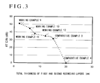
- a 9 mW laser beam was used to record data in the optical recording medium of Working Example 11, whose reproduced signal had a C/N ratio lower than 40 dB when an 8 mW laser beam was used to record data and the C/N ratio of an 8T signal was measured.
- a 10 mW laser beam was used to record data in the optical recording media whose reproduced signals had C/N ratios lower than 40 dB when an 8 mW laser beam was used to record data and the C/N ratio of an 8T signal was measured for each of the optical recording media.
- the C/N ratio of the reproduced signal was lower than 40 dB in the optical recording media of Comparative Examples 3 and 4 in each of which the total thickness of the first recording layer and the second recording layer was equal to or more than 30 nm even when the power of the laser beam used for recording data was increased.
- the C/N ratio of the reproduced signal could be increased to higher than 40 dB by increasing the power of the laser beam used for recording data in each of the optical recording media of Working Examples 11 and 12 in each of which the total thickness of the first recording layer and the second recording layer was equal to or less than 24 nm.
- An optical recording medium was fabricated in the manner of Working Example 1, except that a second recording layer having a thickness of 5 nm and a first recording layer having a thickness of 5 nm were formed.
- An optical recording medium was fabricated in the manner of Working Example 13, except that Mg was added to a second recording layer containing Zn as a primary component.
- An optical recording medium was fabricated in the manner of Working Example 13, except that Al was added to a second recording layer containing Zn as a primary component.
- An optical recording medium was fabricated in the manner of Working Example 13, except that Cu was added to a second recording layer containing Zn as a primary component.
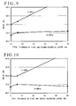
- the noise of an unrecorded region of each of the optical recording media fabricated in accordance with Working Examples 13 to 16 was measured at frequency bands of 16.5 MHz and 4.1 MHz.
- An optical recording medium was fabricated in the manner of Working Example 1, except that a first recording layer containing Si as a primary component and having a thickness of 6 nm was formed and that a second recording layer contained Zn as a primary component and 36 atomic % of Cu added thereto and having a thickness of 6 nm was formed.
- An optical recording medium was fabricated in the manner of Working Example 17, except that a first recording layer having a thickness of 8 nm and a second recording layer having a thickness of 8 nm were formed.
- An optical recording medium was fabricated in the manner of Working Example 17, except that a first recording layer having a thickness of 12 nm and a second recording layer having a thickness of 12 nm were formed.
- An optical recording medium was fabricated in the manner of Working Example 17, except that a first recording layer having a thickness of 15 nm and a second recording layer having a thickness of 15 nm were formed.
- An optical recording medium was fabricated in the manner of Working Example 17, except that a first recording layer having a thickness of 20 nm and a second recording layer having a thickness of 20 nm were formed.
- An optical recording medium sample #A-1 was fabricated in the following manner.
- a polycarbonate substrate having a thickness of 0.6 mm and a diameter of 120 mm was first set on a sputtering apparatus. Then, a second dielectric layer containing a mixture of ZnS and SiO 2 and having a thickness of 60 nm, a second recording layer containing Zn as a primary component and having a thickness of 5 nm, a first recording layer containing Si as a primary component and having a thickness of 5 nm and a first dielectric layer containing the mixture of ZnS and SiO 2 and having a thickness of 60 nm were sequentially formed on the polycarbonate substrate using the sputtering process.
- the mole ratio of ZnS to SiO 2 in the mixture of ZnS and SiO 2 contained in the first dielectric layer and the second dielectric layer was 80:20.
- An optical recording medium sample #A-2 was fabricated in the same manner of the optical recording medium sample #A-1, except that a first recording layer having a thickness of 50 nm and a second recording layer having a thickness of 50 nm were formed.
- An optical recording medium sample #B-1 was fabricated in the manner of Working Example 21, except that a first recording layer containing Zn as a primary component and a second recording layer containing Si as a primary component were formed.
- An optical recording medium sample #B-1 was fabricated in the manner of Comparative Example 6, except that a first recording layer containing Si as a primary component and a second recording layer containing Zn as a primary component were formed.
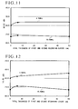
- a laser beam having a wavelength of 635 nm and condensed by an objective lens having a numerical aperture of 0.6 was projected onto each of the optical recording medium samples #A-1, #A-2, #B-1 and #B-2 from the side of the light transmission layer formed by adhering the polycarbonate board and noise at the frequency bands of 16.5 MHz and 4.1 MHz of an unrecorded region of each of the optical recording medium samples was measured at a linear rate of 5.3 m/sec.
- the power of the laser beam was 1.0 mW.
- optical recording medium samples #A-1, #A-2, #B-1 and #B-2 were fabricated in the manner of Working Example 21, Comparative Example 6, Working Example 22 and Comparative Example 7.
- noise at the frequency bands of 16.5 MHz and 4.1 MHz of an unrecorded region of each of the optical recording medium samples was measured in the manner of Working Example 21, Comparative Example 6, Working Example 22 and Comparative Example 7, except that the laser beam was projected onto each of optical recording medium samples via the polycarbonate substrate.
- first recording layer 31 and the second recording layer 32 are formed in contact with each other in the above described embodiment and working examples, it is not absolutely necessary to form the first recording layer 31 and the second recording layer 32 in contact with each other but it is sufficient for the second recording layer 32 to be so located in the vicinity of the first recording layer 31 as to enable formation of a mixed region including the primary component element of the first recording layer 31 and the primary component element of the second recording layer 32 when the region is irradiated with a laser beam. Further, one or more other layers such as a dielectric layer may be interposed between the first recording layer 31 and the second recording layer 32.
- the optical recording medium 10 in the above described embodiment and working examples includes the first recording layer 31 and the second recording layer 32
- the optical recording medium may include one or more recording layers containing an element selected from the group consisting of Si, Ge, C, Sn, Zn, and Cu as a primary component or one or more recording layers containing Al as a primary element, in addition to the first recording layer 31 and the second recording layer 32.
- first recording layer 31 is disposed on the side of the light transmission layer 16 and the second recording layer 32 is disposed on the side of the substrate 11 in the above described embodiment and working examples, it is possible to dispose the first recording layer 31 on the side of the substrate 11 and the second recording layer 32 on the side of the light transmission layer 16.
- the optical recording medium 10 in the above described embodiment and working examples includes the first dielectric layer 15 and the second dielectric layer 13 and the first recording layer 31 and the second recording layer 32 are disposed between the first dielectric layer 15 and the second dielectric layer 13.
- the optical recording medium 10 may include no dielectric layer.
- the optical recording medium 10 may include a single dielectric layer and in such case the dielectric layer may be disposed on either the side of the substrate 11 or the side of the light transmission layer 16 with respect to the first recording layer 31 and the second recording layer 32.
- first recording layer 31 and the second recording layer 32 are formed so as to have the same thickness in the above described embodiment and working examples, it is not absolutely necessary to form the first recording layer 31 and the second recording layer 32 so as to have the same thickness.
- the optical recording medium 10 is provided with the reflective layer 12, if the level of reflected light in the mixed region formed by the mixing an element contained in the first recording layer as a primary component and Zn contained in the second recording layer as a primary component and the level of reflected light in regions onto which the laser beam was not projected greatly differ from each other, the reflective layer may be omitted.
- an optical recording medium constituted so as to record data therein and reproduce data therefrom by projecting a laser beam onto the side opposite to a substrate, including two or more recording layers and being capable of decreasing a noise level and improving a C/N ratio in a reproduced signal.
- optical recording medium which can be fabricated with materials that put minimal load on the environment and has a high long term storage reliability.
Landscapes
- Chemical & Material Sciences (AREA)
- Inorganic Chemistry (AREA)
- Optical Record Carriers And Manufacture Thereof (AREA)
- Thermal Transfer Or Thermal Recording In General (AREA)
Abstract
Description
where at least one kind of an element selected from the group consisting of Mg, Cu and Al is added to the second recording layer 32 containing Zn as a primary component, the surface smoothness of the second recording layer 32 can be much more improved and the noise level of the reproduced signal can be further suppressed.
Modulation Code: (1.7) RLL
Channel Bit Length: 0.12 µm
Recording Linear Velocity: 5.3 m/sec
Channel Clock: 66 MHz
Recording Signal: 8 T
were then reproduced using the optical recording medium evaluation apparatus mentioned above and the C/N ratio of the reproduced signal was measured. When data were reproduced, the wavelength of the laser beam was set at 405 nm, the numerical aperture of the objective lens was set at 0.85 and the power of the laser beam was set at 0.3 mW. The power of the laser beam was defined as the power of the laser beam on the surface of the light transmission layer.
| First Recording Layer | Second Recording Layer | BT C/N (dB) | Judgement | Laser Power (mW) | Judgement | |
| Working Example 1 | Si | Zn | 42.3 | o ○ | 6 | o ○ |
| Working Example 2 | Ge | Zn | 43.1 | o ○ | 5 | o ○ |
| Working Example 3 | C | Zn | 44.5 | o ○ | 8 | o ○ |
| Working Example 4 | Al | Zn | 31.6 | ○ | 10* | ○ |
| Working Example 5 | Zn | Si | 35.3 | ○ | 8 | o ○ |
| Working Example 6 | Zn | Ge | 51.3 | o ○ | 8 | o ○ |
| Working Example 7 | Zn | C | 46.9 | o ○ | 8 | o ○ |
| Working Example 8 | Zn | Al | 43.8 | o ○ | 10* | ○ |
| Comparative Example 1 | W | Zn | Unmeasurable | × | 10* | - |
| Comparative Examples 2 | Zn | W | Unmeasurable | × | 10* | - |
Claims (22)
- An optical recording medium comprising a substrate, a first recording layer formed on the substrate and containing an element selected from the group consisting of Si, Ge, C and Al as a primary component, and a second recording layer located in the vicinity of the first recording layer and containing Zn as a primary component, the optical recording medium being constituted to be irradiated by a laser beam projected onto the side opposite from the substrate and the total thickness of the first recording layer and the second recording layer being equal to or thinner than 30 nm.
- An optical recording medium in accordance with Claim 1 wherein the second recording layer is formed so as to be in contact with the first recording layer.
- An optical recording medium in accordance with Claim 1 or 2 wherein the first recording layer contains an element selected from the group consisting of Si, Ge and C as a primary component.
- An optical recording medium in accordance with any one of Claims 1 to 3 wherein at least one kind of an element selected from the group consisting of Mg, Cu and Al is added to the second recording layer.
- An optical recording medium in accordance with any one of Claims 1 to 4 wherein the first recording layer and the second recording layer are formed so that the total thickness thereof is equal to or thicker than 2 nm.
- An optical recording medium in accordance with Claim 5 wherein the first recording layer and the second recording layer are formed so that the total thickness thereof is 2nm to 24 nm.
- An optical recording medium in accordance with Claim 6 wherein the first recording layer and the second recording layer are formed so that the total thickness thereof is 2nm to 12 nm.
- An optical recording medium in accordance with any one of Claims 1 to 7 which further comprises a light transmission layer provided on a side opposite to the substrate with respect to the first recording layer and the second recording layer, a first dielectric layer provided between the light transmission layer and the first recording layer and the second recording layer, and a second dielectric layer provided between the first recording layer and the second recording layer and the substrate.
- An optical recording medium in accordance with Claim 8 which further comprises a reflective layer provided between the substrate and the second dielectric layer.
- An optical recording medium in accordance with any one of Claims 1 to 9 which is constituted as a write-once type optical recording medium.
- A method for optically recording data comprising a step of projecting a laser beam of predetermined power onto the side opposite from a substrate of an optical recording medium comprising a substrate, a first recording layer formed on the substrate and containing an element selected from the group consisting of Si, Ge, C and Al as a primary component, and a second recording layer located in the vicinity of the first recording layer and containing Zn as a primary component, the optical recording medium being constituted to be irradiated by a laser beam projected onto the side opposite from the substrate and the total thickness of the first recording layer and the second recording layer being equal to or thinner than 30 nm.
- A method for optically recording data in accordance with Claim 11 wherein the second recording layer is formed so as to be in contact with the first recording layer.
- A method for optically recording data in accordance with Claim 11 or 12 wherein the first recording layer contains an element selected from the group consisting of Si, Ge and C as a primary component.
- A method for optically recording data in accordance with any one of Claims 11 to 13 wherein at least one kind of an element selected from the group consisting of Mg, Cu and Al is added to the second recording layer.
- A method for optically recording data in accordance with any one of Claims 11 to 14 wherein the first recording layer and the second recording layer are formed so that the total thickness thereof is equal to or thicker than 2 nm.
- A method for optically recording data in accordance with Claim 15 wherein the first recording layer and the second recording layer are formed so that the total thickness thereof is 2nm to 24 nm.
- A method for optically recording data in accordance with Claim 16 wherein the first recording layer and the second recording layer are formed so that the total thickness thereof is 2nm to 12 nm.
- A method for optically recording data in accordance with any one of Claims 11 to 17 wherein the optical recording medium further comprises a light transmission layer provided on a side opposite to the substrate with respect to the first recording layer and the second recording layer, a first dielectric layer provided between the light transmission layer and the first recording layer and the second recording layer, and a second dielectric layer provided between the first recording layer and the second recording layer and the substrate.
- A method for optically recording data in accordance with Claim 18 wherein the optical recording medium further comprises a reflective layer provided between the substrate and the second dielectric layer.
- A method for optically recording data in accordance with any one of Claims 11 to 19 wherein the optical recording medium is constituted as a write-once type optical recording medium.
- A method for optically recording data in accordance with any one of Claims 11 to 21 which comprises a step of projecting a laser beam having a wavelength of 450 nm or shorter onto the optical recording medium, thereby recording data in the first recording layer and the second recording layer.
- A method for optically recording data in accordance with Claim 21 which comprises steps of employing an objective lens and a laser beam whose numerical aperture NA and wavelength λ satisfy λ/NA ≤ 640 nm, and projecting the laser beam onto the optical recording medium via the objective lens, thereby recording data in the first recording layer and the second recording layer.
Applications Claiming Priority (2)
| Application Number | Priority Date | Filing Date | Title |
|---|---|---|---|
| JP2002128033 | 2002-04-30 | ||
| JP2002128033 | 2002-04-30 |
Publications (2)
| Publication Number | Publication Date |
|---|---|
| EP1359576A2 true EP1359576A2 (en) | 2003-11-05 |
| EP1359576A3 EP1359576A3 (en) | 2005-03-16 |
Family
ID=29208196
Family Applications (1)
| Application Number | Title | Priority Date | Filing Date |
|---|---|---|---|
| EP03009702A Withdrawn EP1359576A3 (en) | 2002-04-30 | 2003-04-30 | Optical recording medium and method for optically recording data on the same |
Country Status (5)
| Country | Link |
|---|---|
| US (1) | US6996055B2 (en) |
| EP (1) | EP1359576A3 (en) |
| KR (1) | KR20030086411A (en) |
| CN (1) | CN1220195C (en) |
| TW (1) | TWI254302B (en) |
Families Citing this family (21)
| Publication number | Priority date | Publication date | Assignee | Title |
|---|---|---|---|---|
| TWI254934B (en) * | 2002-04-26 | 2006-05-11 | Tdk Corp | Optical recording medium and method for optically recording data in the same |
| US20040038080A1 (en) * | 2002-07-01 | 2004-02-26 | Tdk Corporation | Optical recording medium and method for recording data in the same |
| JP4092147B2 (en) * | 2002-07-04 | 2008-05-28 | Tdk株式会社 | Optical recording medium and optical recording method |
| US20040076907A1 (en) * | 2002-10-22 | 2004-04-22 | Tdk Corporation | Optical recording medium and method for manufacturing the same |
| US7781146B2 (en) * | 2002-11-22 | 2010-08-24 | Tdk Corporation | Optical recording medium |
| TWI220523B (en) * | 2003-05-26 | 2004-08-21 | Ritek Corp | Write once recording medium |
| JP2005044396A (en) * | 2003-07-23 | 2005-02-17 | Tdk Corp | Optical information recording medium |
| JP2005071402A (en) * | 2003-08-25 | 2005-03-17 | Tdk Corp | Optical information recording medium |
| KR100694047B1 (en) * | 2004-05-17 | 2007-03-12 | 삼성전자주식회사 | Information storage medium and information recording and reproducing device |
| US7149119B2 (en) * | 2004-09-30 | 2006-12-12 | Matrix Semiconductor, Inc. | System and method of controlling a three-dimensional memory |
| US20070003731A1 (en) * | 2005-06-29 | 2007-01-04 | Micron Technology, Inc. | Gold-semiconductor phase change memory for archival data storage |
| KR100634667B1 (en) * | 2005-08-05 | 2006-10-13 | 엘지전자 주식회사 | Optical recording media |
| US20070092681A1 (en) * | 2005-10-20 | 2007-04-26 | Shuy Geoffrey W | Generating optical contrast using thin layers |
| US20080057257A2 (en) * | 2005-10-20 | 2008-03-06 | Lanyo Technology Co., Ltd. | Contrast Enhancement for Optical Recording |
| US20080057256A2 (en) * | 2005-10-20 | 2008-03-06 | Lanyo Technology Co., Ltd. | Micro-Resonant Structure for Optical Recording |
| US20080056088A2 (en) * | 2005-10-20 | 2008-03-06 | Lanyo Technology Co., Ltd. | Multiple Recording Structures for Optical Recording |
| CN101375333B (en) * | 2005-10-20 | 2013-02-13 | 连宥科技股份有限公司 | Optical contrast using thin layers |
| US20080056089A2 (en) * | 2005-10-20 | 2008-03-06 | Lanyo Technology Co., Ltd. | Generating Optical Contrast Using Thin Layers |
| TW200727289A (en) * | 2006-01-13 | 2007-07-16 | Daxon Technology Inc | Optical storage medium, manufacturing method of recording layer thereof, and recording method thereof |
| TWI328226B (en) * | 2006-08-30 | 2010-08-01 | Cmc Magnetics Corp | The recordable optical recording media |
| US20100110860A1 (en) * | 2008-11-03 | 2010-05-06 | Brigham Young University | Data storage media containing magnesium metal layer |
Family Cites Families (62)
| Publication number | Priority date | Publication date | Assignee | Title |
|---|---|---|---|---|
| US3959799A (en) * | 1974-09-09 | 1976-05-25 | International Business Machines Corporation | Information storage by laser beam initiated reactions |
| US4357616A (en) * | 1979-03-26 | 1982-11-02 | Hitachi, Ltd. | Recording medium |
| JPS5722095A (en) | 1980-07-15 | 1982-02-04 | Nec Corp | Laser beam recording material |
| JPS5727788A (en) | 1980-07-25 | 1982-02-15 | Asahi Chem Ind Co Ltd | Information recording member |
| JPS5816890A (en) | 1981-06-22 | 1983-01-31 | インタ−ナシヨナル・ビジネス・マシ−ンズ・コ−ポレ−シヨン | Optical memory storage medium |
| DE3364607D1 (en) * | 1982-03-15 | 1986-08-28 | Toshiba Kk | Optical type information recording medium |
| US4477819A (en) * | 1982-06-14 | 1984-10-16 | International Business Machines Corporation | Optical recording medium |
| JPS59225992A (en) | 1983-06-06 | 1984-12-19 | Dainippon Ink & Chem Inc | Optical recording medium |
| JPS6028045A (en) * | 1983-07-25 | 1985-02-13 | Sony Corp | Information recording medium |
| JPS60160036A (en) | 1984-01-28 | 1985-08-21 | Toshiba Corp | Optical disk |
| JPS60187933A (en) * | 1984-03-07 | 1985-09-25 | Toshiba Corp | Optical recording and reproducing device |
| JPS60208289A (en) | 1984-03-31 | 1985-10-19 | Dainippon Printing Co Ltd | optical recording material |
| US4670345A (en) * | 1985-02-22 | 1987-06-02 | Asahi Kasei Kogyo Kabushiki Kaisha | Information recording medium |
| JPH0695388B2 (en) * | 1985-06-14 | 1994-11-24 | 株式会社東芝 | Information recording medium |
| JPS62204442A (en) | 1986-03-03 | 1987-09-09 | Toshiba Corp | Optical recording medium and its recording method |
| JPS62245545A (en) | 1986-04-17 | 1987-10-26 | Victor Co Of Japan Ltd | Information recording medium |
| EP0288570B1 (en) * | 1986-10-29 | 1995-06-14 | Dai Nippon Insatsu Kabushiki Kaisha | Draw type optical recording medium |
| JPH01158633A (en) | 1987-12-15 | 1989-06-21 | Toshiba Corp | Information recording medium |
| JPH02152029A (en) | 1988-12-02 | 1990-06-12 | Daicel Chem Ind Ltd | Optical information recording medium |
| JPH0486283A (en) | 1990-07-30 | 1992-03-18 | Sharp Corp | Optical recording material and optical disk |
| EP0474311A1 (en) | 1990-09-06 | 1992-03-11 | Hitachi Maxell Ltd. | Optical data recording medium, method for writing and reading data and apparatus for recording data |
| JP2813844B2 (en) * | 1990-11-22 | 1998-10-22 | ティーディーケイ株式会社 | Optical recording medium |
| JP3163302B2 (en) | 1990-12-29 | 2001-05-08 | 日立マクセル株式会社 | Optical information recording medium and information recording / reproducing method |
| JPH0677510A (en) * | 1992-08-24 | 1994-03-18 | Canon Inc | Photovoltaic element |
| JPH06171236A (en) | 1992-10-05 | 1994-06-21 | Ricoh Co Ltd | Optical recording medium |
| JPH06139621A (en) * | 1992-10-29 | 1994-05-20 | Matsushita Electric Ind Co Ltd | Optical recording medium |
| KR0153033B1 (en) * | 1993-06-18 | 1998-12-15 | 가나이 쯔또무 | Thin film and information recording medium for information recording |
| US5458941A (en) * | 1994-06-09 | 1995-10-17 | Minnesota Mining And Manufacturing Company | Optical recording medium exhibiting eutectic phase equilbria |
| JPH08235641A (en) * | 1995-02-27 | 1996-09-13 | Sony Corp | Optical recording medium and its manufacturing method |
| JP3026327B2 (en) | 1996-07-25 | 2000-03-27 | インダストリアル テクノロジー リサーチ インスティチュート | Write-once optical disc and optical recording medium |
| EP0822543A1 (en) | 1996-07-30 | 1998-02-04 | Industrial Technology Research Institute | Write-once-read-many optical disk |
| US5914214A (en) * | 1996-12-06 | 1999-06-22 | Matsushita Electric Industrial Co., Ltd. | Method for manufacturing an optical information recording medium |
| US6033752A (en) * | 1997-05-22 | 2000-03-07 | Kao Corporation | Optical recording medium and method for recording optical information |
| DE69808240T2 (en) | 1997-10-17 | 2003-06-26 | Kabushiki Kaisha Toyota Chuo Kenkyusho, Aichi | STORAGE ELEMENT |
| JPH11240252A (en) * | 1997-12-22 | 1999-09-07 | Tdk Corp | Photorecording medium |
| KR100598755B1 (en) * | 1998-02-24 | 2006-07-11 | 소니 가부시끼 가이샤 | Optical recording media |
| US6210860B1 (en) * | 1998-04-09 | 2001-04-03 | Kabushiki Kaisha Toyota Chuo Kenkyusho | Recording medium |
| US6254966B1 (en) * | 1998-08-04 | 2001-07-03 | Victor Company Of Japan, Ltd. | Information recording mediums, supporter used in the mediums, manufacture methods of the supporter, manufacturing apparatus of the supporter and stampers for producing the mediums |
| TW448443B (en) | 1998-08-05 | 2001-08-01 | Matsushita Electric Industrial Co Ltd | Optical information storage media and production method as well as the storage reproducing method and device |
| JP2000187884A (en) | 1998-12-21 | 2000-07-04 | Ricoh Co Ltd | Optical recording medium |
| JP2000235732A (en) | 1999-02-12 | 2000-08-29 | Sony Corp | Multilayer optical disc |
| WO2001016947A1 (en) * | 1999-08-31 | 2001-03-08 | Kabushiki Kaisha Toshiba | Optical disk, and method and apparatus for reading data from optical disk |
| JP4339999B2 (en) | 1999-12-20 | 2009-10-07 | パナソニック株式会社 | Optical information recording medium, manufacturing method thereof, recording / reproducing method, and recording / reproducing apparatus |
| TW527585B (en) * | 2000-02-21 | 2003-04-11 | Ind Tech Res Inst | Compact disk device, access method of compact disk, and the compact disk |
| EP1139340B1 (en) | 2000-03-29 | 2004-06-16 | TDK Corporation | Optical recording medium having an oriented silver reflecting layer |
| JP2001344824A (en) * | 2000-03-30 | 2001-12-14 | Tdk Corp | Method for producing optical recording medium and optical recording medium |
| JP2001307393A (en) * | 2000-04-25 | 2001-11-02 | Canon Inc | Magneto-optical reproducing device |
| JP2002157737A (en) | 2000-05-12 | 2002-05-31 | Tdk Corp | Optical recording method and optical recording medium |
| FR2809856B1 (en) | 2000-05-30 | 2002-07-12 | Commissariat Energie Atomique | IRREVERSIBLE OPTICAL RECORDING MEDIA |
| CN1151500C (en) | 2000-06-20 | 2004-05-26 | 财团法人工业技术研究院 | Recordable optical recording medium film and its matching material |
| TW575873B (en) | 2000-07-13 | 2004-02-11 | Matsushita Electric Industrial Co Ltd | Information recording medium, method for producing the same, and recording/reproducing method using the same |
| JP2002050053A (en) | 2000-08-01 | 2002-02-15 | Tdk Corp | Optical information medium |
| JP2002104317A (en) | 2000-09-27 | 2002-04-10 | Strapack Corp | Packing machine |
| JP2002120458A (en) | 2000-10-13 | 2002-04-23 | Ricoh Co Ltd | Write-once optical recording medium |
| TWI246681B (en) * | 2000-12-15 | 2006-01-01 | Koninkl Philips Electronics Nv | Optical information medium and its use |
| JP2002269808A (en) | 2001-03-09 | 2002-09-20 | Ricoh Co Ltd | Optical information recording medium |
| JP2003054135A (en) | 2001-06-05 | 2003-02-26 | Tdk Corp | Optical recording medium and optical recording method |
| JP2003085778A (en) | 2001-06-29 | 2003-03-20 | Sony Corp | Optical recording / reproducing medium, mother stamper for manufacturing optical recording / reproducing medium, and optical recording / reproducing device |
| TWI254301B (en) * | 2002-04-05 | 2006-05-01 | Tdk Corp | Optical recording medium and method for optically recording information in the same |
| TWI254934B (en) * | 2002-04-26 | 2006-05-11 | Tdk Corp | Optical recording medium and method for optically recording data in the same |
| JP4092147B2 (en) * | 2002-07-04 | 2008-05-28 | Tdk株式会社 | Optical recording medium and optical recording method |
| JP4084674B2 (en) * | 2003-01-28 | 2008-04-30 | Tdk株式会社 | Optical recording medium |
-
2003
- 2003-04-29 CN CNB031423159A patent/CN1220195C/en not_active Expired - Fee Related
- 2003-04-29 US US10/425,571 patent/US6996055B2/en not_active Expired - Fee Related
- 2003-04-30 TW TW092110199A patent/TWI254302B/en not_active IP Right Cessation
- 2003-04-30 EP EP03009702A patent/EP1359576A3/en not_active Withdrawn
- 2003-04-30 KR KR10-2003-0027532A patent/KR20030086411A/en not_active Ceased
Also Published As
| Publication number | Publication date |
|---|---|
| TWI254302B (en) | 2006-05-01 |
| EP1359576A3 (en) | 2005-03-16 |
| US6996055B2 (en) | 2006-02-07 |
| TW200401282A (en) | 2004-01-16 |
| CN1455401A (en) | 2003-11-12 |
| CN1220195C (en) | 2005-09-21 |
| KR20030086411A (en) | 2003-11-10 |
| US20030231577A1 (en) | 2003-12-18 |
Similar Documents
| Publication | Publication Date | Title |
|---|---|---|
| US7479363B2 (en) | Optical recording medium and method for optically recording data in the same | |
| US6996055B2 (en) | Optical recording medium and method for optically recording data in the same | |
| US7276274B2 (en) | Optical recording medium and method for recording and reproducing data | |
| US7018695B2 (en) | Optical recording medium | |
| US20040157158A1 (en) | Optical recording medium | |
| US6929840B2 (en) | Optical recording medium, method for manufacturing the same and target used for sputtering process | |
| EP1351230A2 (en) | Optical recording medium and method for optically recording information on the same | |
| EP1394786A1 (en) | Optical recording medium and method for optically recording data in the same | |
| US7014903B2 (en) | Optical recording medium | |
| US7018694B2 (en) | Optical recording medium, method for manufacturing the same and target used for sputtering process | |
| US7231649B2 (en) | Optical recording medium and method for optically recording data in the same | |
| US20040076907A1 (en) | Optical recording medium and method for manufacturing the same | |
| US7781146B2 (en) | Optical recording medium | |
| KR100731472B1 (en) | Optical record reproducing method and optical recording medium | |
| KR20030094051A (en) | Optical recording and playback method, and optical recording media | |
| US20070122583A1 (en) | Optical recording disc and method for manufacturing optical recording disc | |
| JP4084695B2 (en) | Optical recording medium and optical recording method | |
| JP4105589B2 (en) | Optical recording medium and optical recording method | |
| JP4319456B2 (en) | Optical recording medium and optical recording method |
Legal Events
| Date | Code | Title | Description |
|---|---|---|---|
| PUAI | Public reference made under article 153(3) epc to a published international application that has entered the european phase |
Free format text: ORIGINAL CODE: 0009012 |
|
| AK | Designated contracting states |
Kind code of ref document: A2 Designated state(s): AT BE BG CH CY CZ DE DK EE ES FI FR GB GR HU IE IT LI LU MC NL PT RO SE SI SK TR |
|
| AX | Request for extension of the european patent |
Extension state: AL LT LV MK |
|
| PUAL | Search report despatched |
Free format text: ORIGINAL CODE: 0009013 |
|
| AK | Designated contracting states |
Kind code of ref document: A3 Designated state(s): AT BE BG CH CY CZ DE DK EE ES FI FR GB GR HU IE IT LI LU MC NL PT RO SE SI SK TR |
|
| AX | Request for extension of the european patent |
Extension state: AL LT LV MK |
|
| RIC1 | Information provided on ipc code assigned before grant |
Ipc: 7G 11B 7/0045 B Ipc: 7G 11B 7/24 A |
|
| 17P | Request for examination filed |
Effective date: 20050615 |
|
| AKX | Designation fees paid |
Designated state(s): AT BE BG CH CY CZ DE DK EE ES FI FR GB GR HU IE IT LI LU MC NL PT RO SE SI SK TR |
|
| STAA | Information on the status of an ep patent application or granted ep patent |
Free format text: STATUS: THE APPLICATION IS DEEMED TO BE WITHDRAWN |
|
| 18D | Application deemed to be withdrawn |
Effective date: 20051125 |