EP1357613A2 - Efficient electroluminescent device - Google Patents
Efficient electroluminescent device Download PDFInfo
- Publication number
- EP1357613A2 EP1357613A2 EP03076076A EP03076076A EP1357613A2 EP 1357613 A2 EP1357613 A2 EP 1357613A2 EP 03076076 A EP03076076 A EP 03076076A EP 03076076 A EP03076076 A EP 03076076A EP 1357613 A2 EP1357613 A2 EP 1357613A2
- Authority
- EP
- European Patent Office
- Prior art keywords
- compound
- host
- light emitting
- layer
- emitting layer
- Prior art date
- Legal status (The legal status is an assumption and is not a legal conclusion. Google has not performed a legal analysis and makes no representation as to the accuracy of the status listed.)
- Withdrawn
Links
- 239000002019 doping agent Substances 0.000 claims abstract description 34
- 150000001875 compounds Chemical class 0.000 claims abstract description 24
- YTUILTQRCVAYNB-UHFFFAOYSA-N 101686-49-1 Chemical group C=12C3=CC=CC2=CC=CC=1C1=CC=C2C4=CC=CC=C4C4=CC=C3C1=C42 YTUILTQRCVAYNB-UHFFFAOYSA-N 0.000 claims abstract description 10
- -1 indenoperylene compound Chemical class 0.000 claims description 99
- 239000000463 material Substances 0.000 claims description 52
- 125000001424 substituent group Chemical group 0.000 claims description 32
- TVIVIEFSHFOWTE-UHFFFAOYSA-K tri(quinolin-8-yloxy)alumane Chemical compound [Al+3].C1=CN=C2C([O-])=CC=CC2=C1.C1=CN=C2C([O-])=CC=CC2=C1.C1=CN=C2C([O-])=CC=CC2=C1 TVIVIEFSHFOWTE-UHFFFAOYSA-K 0.000 claims description 21
- 125000003118 aryl group Chemical group 0.000 claims description 19
- OBAJPWYDYFEBTF-UHFFFAOYSA-N 2-tert-butyl-9,10-dinaphthalen-2-ylanthracene Chemical compound C1=CC=CC2=CC(C3=C4C=CC=CC4=C(C=4C=C5C=CC=CC5=CC=4)C4=CC=C(C=C43)C(C)(C)C)=CC=C21 OBAJPWYDYFEBTF-UHFFFAOYSA-N 0.000 claims description 17
- 229910052739 hydrogen Inorganic materials 0.000 claims description 10
- 239000001257 hydrogen Substances 0.000 claims description 10
- UFHFLCQGNIYNRP-UHFFFAOYSA-N Hydrogen Chemical compound [H][H] UFHFLCQGNIYNRP-UHFFFAOYSA-N 0.000 claims description 8
- MWPLVEDNUUSJAV-UHFFFAOYSA-N anthracene Natural products C1=CC=CC2=CC3=CC=CC=C3C=C21 MWPLVEDNUUSJAV-UHFFFAOYSA-N 0.000 claims description 8
- SIKJAQJRHWYJAI-UHFFFAOYSA-N benzopyrrole Natural products C1=CC=C2NC=CC2=C1 SIKJAQJRHWYJAI-UHFFFAOYSA-N 0.000 claims description 8
- 229910052799 carbon Inorganic materials 0.000 claims description 8
- OKTJSMMVPCPJKN-UHFFFAOYSA-N Carbon Chemical compound [C] OKTJSMMVPCPJKN-UHFFFAOYSA-N 0.000 claims description 7
- 125000005842 heteroatom Chemical group 0.000 claims description 5
- 230000000903 blocking effect Effects 0.000 claims description 3
- GEQBRULPNIVQPP-UHFFFAOYSA-N 2-[3,5-bis(1-phenylbenzimidazol-2-yl)phenyl]-1-phenylbenzimidazole Chemical compound C1=CC=CC=C1N1C2=CC=CC=C2N=C1C1=CC(C=2N(C3=CC=CC=C3N=2)C=2C=CC=CC=2)=CC(C=2N(C3=CC=CC=C3N=2)C=2C=CC=CC=2)=C1 GEQBRULPNIVQPP-UHFFFAOYSA-N 0.000 claims description 2
- 125000004122 cyclic group Chemical group 0.000 claims description 2
- 239000010410 layer Substances 0.000 description 80
- 229910052751 metal Inorganic materials 0.000 description 16
- 239000002184 metal Substances 0.000 description 16
- 125000004432 carbon atom Chemical group C* 0.000 description 14
- IJGRMHOSHXDMSA-UHFFFAOYSA-N nitrogen Substances N#N IJGRMHOSHXDMSA-UHFFFAOYSA-N 0.000 description 13
- YXFVVABEGXRONW-UHFFFAOYSA-N Toluene Chemical compound CC1=CC=CC=C1 YXFVVABEGXRONW-UHFFFAOYSA-N 0.000 description 12
- 239000000758 substrate Substances 0.000 description 12
- 229910052715 tantalum Inorganic materials 0.000 description 12
- GUVRBAGPIYLISA-UHFFFAOYSA-N tantalum atom Chemical compound [Ta] GUVRBAGPIYLISA-UHFFFAOYSA-N 0.000 description 12
- YBYIRNPNPLQARY-UHFFFAOYSA-N 1H-indene Chemical compound C1=CC=C2CC=CC2=C1 YBYIRNPNPLQARY-UHFFFAOYSA-N 0.000 description 11
- 125000000217 alkyl group Chemical group 0.000 description 11
- 238000000151 deposition Methods 0.000 description 10
- 230000008021 deposition Effects 0.000 description 10
- 125000004429 atom Chemical group 0.000 description 9
- 239000012044 organic layer Substances 0.000 description 9
- 125000005259 triarylamine group Chemical group 0.000 description 9
- 125000000623 heterocyclic group Chemical group 0.000 description 8
- 230000006872 improvement Effects 0.000 description 8
- 229910052757 nitrogen Inorganic materials 0.000 description 8
- QVGXLLKOCUKJST-UHFFFAOYSA-N atomic oxygen Chemical compound [O] QVGXLLKOCUKJST-UHFFFAOYSA-N 0.000 description 7
- 238000005401 electroluminescence Methods 0.000 description 7
- 229910052760 oxygen Inorganic materials 0.000 description 7
- 239000001301 oxygen Substances 0.000 description 7
- MCJGNVYPOGVAJF-UHFFFAOYSA-N quinolin-8-ol Chemical compound C1=CN=C2C(O)=CC=CC2=C1 MCJGNVYPOGVAJF-UHFFFAOYSA-N 0.000 description 7
- YMWUJEATGCHHMB-UHFFFAOYSA-N Dichloromethane Chemical compound ClCCl YMWUJEATGCHHMB-UHFFFAOYSA-N 0.000 description 6
- UFWIBTONFRDIAS-UHFFFAOYSA-N Naphthalene Chemical compound C1=CC=CC2=CC=CC=C21 UFWIBTONFRDIAS-UHFFFAOYSA-N 0.000 description 6
- 230000000052 comparative effect Effects 0.000 description 6
- NBVXSUQYWXRMNV-UHFFFAOYSA-N fluoromethane Chemical compound FC NBVXSUQYWXRMNV-UHFFFAOYSA-N 0.000 description 6
- WIAWDMBHXUZQGV-UHFFFAOYSA-N heptacyclo[13.10.1.12,6.011,26.017,25.018,23.010,27]heptacosa-1(25),2,4,6(27),7,9,11,13,15(26),17,19,21,23-tridecaene Chemical group C=12C3=CC=CC2=CC=CC=1C1=CC=CC2=C1C3=C1C=C3C=CC=CC3=C1C2 WIAWDMBHXUZQGV-UHFFFAOYSA-N 0.000 description 6
- 238000002347 injection Methods 0.000 description 6
- 239000007924 injection Substances 0.000 description 6
- 239000011777 magnesium Substances 0.000 description 6
- 125000002080 perylenyl group Chemical group C1(=CC=C2C=CC=C3C4=CC=CC5=CC=CC(C1=C23)=C45)* 0.000 description 6
- 230000006798 recombination Effects 0.000 description 6
- 238000005215 recombination Methods 0.000 description 6
- 239000007983 Tris buffer Substances 0.000 description 5
- 125000003545 alkoxy group Chemical group 0.000 description 5
- 125000000732 arylene group Chemical group 0.000 description 5
- 239000010406 cathode material Substances 0.000 description 5
- 239000011521 glass Substances 0.000 description 5
- 229910052749 magnesium Inorganic materials 0.000 description 5
- 125000001997 phenyl group Chemical group [H]C1=C([H])C([H])=C(*)C([H])=C1[H] 0.000 description 5
- 239000000126 substance Substances 0.000 description 5
- XLYOFNOQVPJJNP-UHFFFAOYSA-N water Substances O XLYOFNOQVPJJNP-UHFFFAOYSA-N 0.000 description 5
- LFQSCWFLJHTTHZ-UHFFFAOYSA-N Ethanol Chemical compound CCO LFQSCWFLJHTTHZ-UHFFFAOYSA-N 0.000 description 4
- NRCMAYZCPIVABH-UHFFFAOYSA-N Quinacridone Chemical class N1C2=CC=CC=C2C(=O)C2=C1C=C1C(=O)C3=CC=CC=C3NC1=C2 NRCMAYZCPIVABH-UHFFFAOYSA-N 0.000 description 4
- HEDRZPFGACZZDS-MICDWDOJSA-N Trichloro(2H)methane Chemical compound [2H]C(Cl)(Cl)Cl HEDRZPFGACZZDS-MICDWDOJSA-N 0.000 description 4
- 229910052782 aluminium Inorganic materials 0.000 description 4
- XAGFODPZIPBFFR-UHFFFAOYSA-N aluminium Chemical compound [Al] XAGFODPZIPBFFR-UHFFFAOYSA-N 0.000 description 4
- REDXJYDRNCIFBQ-UHFFFAOYSA-N aluminium(3+) Chemical compound [Al+3] REDXJYDRNCIFBQ-UHFFFAOYSA-N 0.000 description 4
- 125000004104 aryloxy group Chemical group 0.000 description 4
- 238000011156 evaluation Methods 0.000 description 4
- AMGQUBHHOARCQH-UHFFFAOYSA-N indium;oxotin Chemical compound [In].[Sn]=O AMGQUBHHOARCQH-UHFFFAOYSA-N 0.000 description 4
- 238000000034 method Methods 0.000 description 4
- 239000000203 mixture Substances 0.000 description 4
- IBHBKWKFFTZAHE-UHFFFAOYSA-N n-[4-[4-(n-naphthalen-1-ylanilino)phenyl]phenyl]-n-phenylnaphthalen-1-amine Chemical group C1=CC=CC=C1N(C=1C2=CC=CC=C2C=CC=1)C1=CC=C(C=2C=CC(=CC=2)N(C=2C=CC=CC=2)C=2C3=CC=CC=C3C=CC=2)C=C1 IBHBKWKFFTZAHE-UHFFFAOYSA-N 0.000 description 4
- 125000001624 naphthyl group Chemical group 0.000 description 4
- 229910052709 silver Inorganic materials 0.000 description 4
- 238000012546 transfer Methods 0.000 description 4
- 238000005160 1H NMR spectroscopy Methods 0.000 description 3
- QGJOPFRUJISHPQ-UHFFFAOYSA-N Carbon disulfide Chemical compound S=C=S QGJOPFRUJISHPQ-UHFFFAOYSA-N 0.000 description 3
- XPDWGBQVDMORPB-UHFFFAOYSA-N Fluoroform Chemical group FC(F)F XPDWGBQVDMORPB-UHFFFAOYSA-N 0.000 description 3
- GYHNNYVSQQEPJS-UHFFFAOYSA-N Gallium Chemical compound [Ga] GYHNNYVSQQEPJS-UHFFFAOYSA-N 0.000 description 3
- NINIDFKCEFEMDL-UHFFFAOYSA-N Sulfur Chemical compound [S] NINIDFKCEFEMDL-UHFFFAOYSA-N 0.000 description 3
- QCWXUUIWCKQGHC-UHFFFAOYSA-N Zirconium Chemical compound [Zr] QCWXUUIWCKQGHC-UHFFFAOYSA-N 0.000 description 3
- 125000002947 alkylene group Chemical group 0.000 description 3
- 239000010405 anode material Substances 0.000 description 3
- 125000005605 benzo group Chemical group 0.000 description 3
- 230000015572 biosynthetic process Effects 0.000 description 3
- 238000005229 chemical vapour deposition Methods 0.000 description 3
- 239000004020 conductor Substances 0.000 description 3
- 239000008367 deionised water Substances 0.000 description 3
- 229910021641 deionized water Inorganic materials 0.000 description 3
- 239000003599 detergent Substances 0.000 description 3
- 229910052733 gallium Inorganic materials 0.000 description 3
- 229910052736 halogen Inorganic materials 0.000 description 3
- 150000002367 halogens Chemical class 0.000 description 3
- 238000004519 manufacturing process Methods 0.000 description 3
- 229960003540 oxyquinoline Drugs 0.000 description 3
- CSHWQDPOILHKBI-UHFFFAOYSA-N peryrene Natural products C1=CC(C2=CC=CC=3C2=C2C=CC=3)=C3C2=CC=CC3=C1 CSHWQDPOILHKBI-UHFFFAOYSA-N 0.000 description 3
- 125000000843 phenylene group Chemical group C1(=C(C=CC=C1)*)* 0.000 description 3
- 125000003367 polycyclic group Chemical group 0.000 description 3
- 238000002360 preparation method Methods 0.000 description 3
- 239000000243 solution Substances 0.000 description 3
- 229910052717 sulfur Inorganic materials 0.000 description 3
- 239000011593 sulfur Substances 0.000 description 3
- 229910052726 zirconium Inorganic materials 0.000 description 3
- LQRAULANJCQXAM-UHFFFAOYSA-N 1-n,5-n-dinaphthalen-1-yl-1-n,5-n-diphenylnaphthalene-1,5-diamine Chemical compound C1=CC=CC=C1N(C=1C2=CC=CC(=C2C=CC=1)N(C=1C=CC=CC=1)C=1C2=CC=CC=C2C=CC=1)C1=CC=CC2=CC=CC=C12 LQRAULANJCQXAM-UHFFFAOYSA-N 0.000 description 2
- 239000005725 8-Hydroxyquinoline Substances 0.000 description 2
- VIZUPBYFLORCRA-UHFFFAOYSA-N 9,10-dinaphthalen-2-ylanthracene Chemical class C12=CC=CC=C2C(C2=CC3=CC=CC=C3C=C2)=C(C=CC=C2)C2=C1C1=CC=C(C=CC=C2)C2=C1 VIZUPBYFLORCRA-UHFFFAOYSA-N 0.000 description 2
- XKRFYHLGVUSROY-UHFFFAOYSA-N Argon Chemical compound [Ar] XKRFYHLGVUSROY-UHFFFAOYSA-N 0.000 description 2
- ZOXJGFHDIHLPTG-UHFFFAOYSA-N Boron Chemical compound [B] ZOXJGFHDIHLPTG-UHFFFAOYSA-N 0.000 description 2
- PXGOKWXKJXAPGV-UHFFFAOYSA-N Fluorine Chemical compound FF PXGOKWXKJXAPGV-UHFFFAOYSA-N 0.000 description 2
- WHXSMMKQMYFTQS-UHFFFAOYSA-N Lithium Chemical compound [Li] WHXSMMKQMYFTQS-UHFFFAOYSA-N 0.000 description 2
- FYYHWMGAXLPEAU-UHFFFAOYSA-N Magnesium Chemical compound [Mg] FYYHWMGAXLPEAU-UHFFFAOYSA-N 0.000 description 2
- CSNNHWWHGAXBCP-UHFFFAOYSA-L Magnesium sulfate Chemical compound [Mg+2].[O-][S+2]([O-])([O-])[O-] CSNNHWWHGAXBCP-UHFFFAOYSA-L 0.000 description 2
- KDLHZDBZIXYQEI-UHFFFAOYSA-N Palladium Chemical compound [Pd] KDLHZDBZIXYQEI-UHFFFAOYSA-N 0.000 description 2
- 229920001609 Poly(3,4-ethylenedioxythiophene) Polymers 0.000 description 2
- KAESVJOAVNADME-UHFFFAOYSA-N Pyrrole Chemical compound C=1C=CNC=1 KAESVJOAVNADME-UHFFFAOYSA-N 0.000 description 2
- VYPSYNLAJGMNEJ-UHFFFAOYSA-N Silicium dioxide Chemical compound O=[Si]=O VYPSYNLAJGMNEJ-UHFFFAOYSA-N 0.000 description 2
- CDBYLPFSWZWCQE-UHFFFAOYSA-L Sodium Carbonate Chemical compound [Na+].[Na+].[O-]C([O-])=O CDBYLPFSWZWCQE-UHFFFAOYSA-L 0.000 description 2
- XLOMVQKBTHCTTD-UHFFFAOYSA-N Zinc monoxide Chemical compound [Zn]=O XLOMVQKBTHCTTD-UHFFFAOYSA-N 0.000 description 2
- 230000008901 benefit Effects 0.000 description 2
- 229910052796 boron Inorganic materials 0.000 description 2
- IAQRGUVFOMOMEM-UHFFFAOYSA-N but-2-ene Chemical compound CC=CC IAQRGUVFOMOMEM-UHFFFAOYSA-N 0.000 description 2
- OSGAYBCDTDRGGQ-UHFFFAOYSA-L calcium sulfate Chemical compound [Ca+2].[O-]S([O-])(=O)=O OSGAYBCDTDRGGQ-UHFFFAOYSA-L 0.000 description 2
- 125000002837 carbocyclic group Chemical group 0.000 description 2
- 125000001309 chloro group Chemical group Cl* 0.000 description 2
- ORTQZVOHEJQUHG-UHFFFAOYSA-L copper(II) chloride Chemical compound Cl[Cu]Cl ORTQZVOHEJQUHG-UHFFFAOYSA-L 0.000 description 2
- 125000000753 cycloalkyl group Chemical group 0.000 description 2
- 230000003247 decreasing effect Effects 0.000 description 2
- 239000000975 dye Substances 0.000 description 2
- 238000005538 encapsulation Methods 0.000 description 2
- 125000001495 ethyl group Chemical group [H]C([H])([H])C([H])([H])* 0.000 description 2
- 230000008020 evaporation Effects 0.000 description 2
- 238000001704 evaporation Methods 0.000 description 2
- 239000010408 film Substances 0.000 description 2
- GVEPBJHOBDJJJI-UHFFFAOYSA-N fluoranthene Chemical compound C1=CC(C2=CC=CC=C22)=C3C2=CC=CC3=C1 GVEPBJHOBDJJJI-UHFFFAOYSA-N 0.000 description 2
- 229910052731 fluorine Inorganic materials 0.000 description 2
- 239000011737 fluorine Substances 0.000 description 2
- 125000001153 fluoro group Chemical group F* 0.000 description 2
- 125000002541 furyl group Chemical group 0.000 description 2
- 230000004927 fusion Effects 0.000 description 2
- 150000004820 halides Chemical class 0.000 description 2
- BHEPBYXIRTUNPN-UHFFFAOYSA-N hydridophosphorus(.) (triplet) Chemical compound [PH] BHEPBYXIRTUNPN-UHFFFAOYSA-N 0.000 description 2
- 150000002431 hydrogen Chemical class 0.000 description 2
- 229910052738 indium Inorganic materials 0.000 description 2
- APFVFJFRJDLVQX-UHFFFAOYSA-N indium atom Chemical compound [In] APFVFJFRJDLVQX-UHFFFAOYSA-N 0.000 description 2
- 229910052744 lithium Inorganic materials 0.000 description 2
- 238000004020 luminiscence type Methods 0.000 description 2
- 239000011159 matrix material Substances 0.000 description 2
- 229910044991 metal oxide Inorganic materials 0.000 description 2
- 150000004706 metal oxides Chemical class 0.000 description 2
- UHVLDCDWBKWDDN-UHFFFAOYSA-N n-phenyl-n-[4-[4-(n-pyren-2-ylanilino)phenyl]phenyl]pyren-2-amine Chemical group C1=CC=CC=C1N(C=1C=C2C=CC3=CC=CC4=CC=C(C2=C43)C=1)C1=CC=C(C=2C=CC(=CC=2)N(C=2C=CC=CC=2)C=2C=C3C=CC4=CC=CC5=CC=C(C3=C54)C=2)C=C1 UHVLDCDWBKWDDN-UHFFFAOYSA-N 0.000 description 2
- 239000011368 organic material Substances 0.000 description 2
- NFHFRUOZVGFOOS-UHFFFAOYSA-N palladium;triphenylphosphane Chemical compound [Pd].C1=CC=CC=C1P(C=1C=CC=CC=1)C1=CC=CC=C1.C1=CC=CC=C1P(C=1C=CC=CC=1)C1=CC=CC=C1.C1=CC=CC=C1P(C=1C=CC=CC=1)C1=CC=CC=C1.C1=CC=CC=C1P(C=1C=CC=CC=1)C1=CC=CC=C1 NFHFRUOZVGFOOS-UHFFFAOYSA-N 0.000 description 2
- BASFCYQUMIYNBI-UHFFFAOYSA-N platinum Chemical compound [Pt] BASFCYQUMIYNBI-UHFFFAOYSA-N 0.000 description 2
- 229920003227 poly(N-vinyl carbazole) Polymers 0.000 description 2
- 125000004076 pyridyl group Chemical group 0.000 description 2
- 125000002943 quinolinyl group Chemical group N1=C(C=CC2=CC=CC=C12)* 0.000 description 2
- 239000000741 silica gel Substances 0.000 description 2
- 229910002027 silica gel Inorganic materials 0.000 description 2
- 229960001866 silicon dioxide Drugs 0.000 description 2
- 239000007787 solid Substances 0.000 description 2
- 239000002904 solvent Substances 0.000 description 2
- 238000004544 sputter deposition Methods 0.000 description 2
- 238000000859 sublimation Methods 0.000 description 2
- 230000008022 sublimation Effects 0.000 description 2
- 125000000999 tert-butyl group Chemical group [H]C([H])([H])C(*)(C([H])([H])[H])C([H])([H])[H] 0.000 description 2
- 125000001544 thienyl group Chemical group 0.000 description 2
- 239000010409 thin film Substances 0.000 description 2
- 125000004149 thio group Chemical group *S* 0.000 description 2
- 229910052723 transition metal Inorganic materials 0.000 description 2
- 150000003624 transition metals Chemical class 0.000 description 2
- PFNQVRZLDWYSCW-UHFFFAOYSA-N (fluoren-9-ylideneamino) n-naphthalen-1-ylcarbamate Chemical compound C12=CC=CC=C2C2=CC=CC=C2C1=NOC(=O)NC1=CC=CC2=CC=CC=C12 PFNQVRZLDWYSCW-UHFFFAOYSA-N 0.000 description 1
- BRSRUYVJULRMRQ-UHFFFAOYSA-N 1-phenylanthracene Chemical class C1=CC=CC=C1C1=CC=CC2=CC3=CC=CC=C3C=C12 BRSRUYVJULRMRQ-UHFFFAOYSA-N 0.000 description 1
- XNCMQRWVMWLODV-UHFFFAOYSA-N 1-phenylbenzimidazole Chemical compound C1=NC2=CC=CC=C2N1C1=CC=CC=C1 XNCMQRWVMWLODV-UHFFFAOYSA-N 0.000 description 1
- 125000002941 2-furyl group Chemical group O1C([*])=C([H])C([H])=C1[H] 0.000 description 1
- MVLOINQUZSPUJS-UHFFFAOYSA-N 2-n,2-n,6-n,6-n-tetrakis(4-methylphenyl)naphthalene-2,6-diamine Chemical compound C1=CC(C)=CC=C1N(C=1C=C2C=CC(=CC2=CC=1)N(C=1C=CC(C)=CC=1)C=1C=CC(C)=CC=1)C1=CC=C(C)C=C1 MVLOINQUZSPUJS-UHFFFAOYSA-N 0.000 description 1
- MATLFWDVOBGZFG-UHFFFAOYSA-N 2-n,2-n,6-n,6-n-tetranaphthalen-1-ylnaphthalene-2,6-diamine Chemical compound C1=CC=C2C(N(C=3C=C4C=CC(=CC4=CC=3)N(C=3C4=CC=CC=C4C=CC=3)C=3C4=CC=CC=C4C=CC=3)C=3C4=CC=CC=C4C=CC=3)=CC=CC2=C1 MATLFWDVOBGZFG-UHFFFAOYSA-N 0.000 description 1
- VXJRNCUNIBHMKV-UHFFFAOYSA-N 2-n,6-n-dinaphthalen-1-yl-2-n,6-n-dinaphthalen-2-ylnaphthalene-2,6-diamine Chemical compound C1=CC=C2C(N(C=3C=C4C=CC(=CC4=CC=3)N(C=3C=C4C=CC=CC4=CC=3)C=3C4=CC=CC=C4C=CC=3)C3=CC4=CC=CC=C4C=C3)=CC=CC2=C1 VXJRNCUNIBHMKV-UHFFFAOYSA-N 0.000 description 1
- KYGSXEYUWRFVNY-UHFFFAOYSA-N 2-pyran-2-ylidenepropanedinitrile Chemical compound N#CC(C#N)=C1OC=CC=C1 KYGSXEYUWRFVNY-UHFFFAOYSA-N 0.000 description 1
- 125000000175 2-thienyl group Chemical group S1C([*])=C([H])C([H])=C1[H] 0.000 description 1
- GOLORTLGFDVFDW-UHFFFAOYSA-N 3-(1h-benzimidazol-2-yl)-7-(diethylamino)chromen-2-one Chemical compound C1=CC=C2NC(C3=CC4=CC=C(C=C4OC3=O)N(CC)CC)=NC2=C1 GOLORTLGFDVFDW-UHFFFAOYSA-N 0.000 description 1
- MBWSEPXTVAGLJS-UHFFFAOYSA-N 3-bromo-7,12-diphenylbenzo[k]fluoranthene Chemical compound C=12C3=CC=CC=1C(Br)=CC=C2C(C(=C1C=CC=CC1=1)C=2C=CC=CC=2)=C3C=1C1=CC=CC=C1 MBWSEPXTVAGLJS-UHFFFAOYSA-N 0.000 description 1
- AHDTYXOIJHCGKH-UHFFFAOYSA-N 4-[[4-(dimethylamino)-2-methylphenyl]-phenylmethyl]-n,n,3-trimethylaniline Chemical compound CC1=CC(N(C)C)=CC=C1C(C=1C(=CC(=CC=1)N(C)C)C)C1=CC=CC=C1 AHDTYXOIJHCGKH-UHFFFAOYSA-N 0.000 description 1
- YXYUIABODWXVIK-UHFFFAOYSA-N 4-methyl-n,n-bis(4-methylphenyl)aniline Chemical compound C1=CC(C)=CC=C1N(C=1C=CC(C)=CC=1)C1=CC=C(C)C=C1 YXYUIABODWXVIK-UHFFFAOYSA-N 0.000 description 1
- MEIBOBDKQKIBJH-UHFFFAOYSA-N 4-methyl-n-[4-[1-[4-(4-methyl-n-(4-methylphenyl)anilino)phenyl]-4-phenylcyclohexyl]phenyl]-n-(4-methylphenyl)aniline Chemical compound C1=CC(C)=CC=C1N(C=1C=CC(=CC=1)C1(CCC(CC1)C=1C=CC=CC=1)C=1C=CC(=CC=1)N(C=1C=CC(C)=CC=1)C=1C=CC(C)=CC=1)C1=CC=C(C)C=C1 MEIBOBDKQKIBJH-UHFFFAOYSA-N 0.000 description 1
- ZOKIJILZFXPFTO-UHFFFAOYSA-N 4-methyl-n-[4-[1-[4-(4-methyl-n-(4-methylphenyl)anilino)phenyl]cyclohexyl]phenyl]-n-(4-methylphenyl)aniline Chemical compound C1=CC(C)=CC=C1N(C=1C=CC(=CC=1)C1(CCCCC1)C=1C=CC(=CC=1)N(C=1C=CC(C)=CC=1)C=1C=CC(C)=CC=1)C1=CC=C(C)C=C1 ZOKIJILZFXPFTO-UHFFFAOYSA-N 0.000 description 1
- LQYYDWJDEVKDGB-UHFFFAOYSA-N 4-methyl-n-[4-[2-[4-[2-[4-(4-methyl-n-(4-methylphenyl)anilino)phenyl]ethenyl]phenyl]ethenyl]phenyl]-n-(4-methylphenyl)aniline Chemical compound C1=CC(C)=CC=C1N(C=1C=CC(C=CC=2C=CC(C=CC=3C=CC(=CC=3)N(C=3C=CC(C)=CC=3)C=3C=CC(C)=CC=3)=CC=2)=CC=1)C1=CC=C(C)C=C1 LQYYDWJDEVKDGB-UHFFFAOYSA-N 0.000 description 1
- QCRMNYVCABKJCM-UHFFFAOYSA-N 5-methyl-2h-pyran Chemical compound CC1=COCC=C1 QCRMNYVCABKJCM-UHFFFAOYSA-N 0.000 description 1
- 125000003341 7 membered heterocyclic group Chemical group 0.000 description 1
- BITWULPDIGXQDL-UHFFFAOYSA-N 9,10-bis[4-(2,2-diphenylethenyl)phenyl]anthracene Chemical class C=1C=C(C=2C3=CC=CC=C3C(C=3C=CC(C=C(C=4C=CC=CC=4)C=4C=CC=CC=4)=CC=3)=C3C=CC=CC3=2)C=CC=1C=C(C=1C=CC=CC=1)C1=CC=CC=C1 BITWULPDIGXQDL-UHFFFAOYSA-N 0.000 description 1
- VIJYEGDOKCKUOL-UHFFFAOYSA-N 9-phenylcarbazole Chemical compound C1=CC=CC=C1N1C2=CC=CC=C2C2=CC=CC=C21 VIJYEGDOKCKUOL-UHFFFAOYSA-N 0.000 description 1
- GJCOSYZMQJWQCA-UHFFFAOYSA-N 9H-xanthene Chemical compound C1=CC=C2CC3=CC=CC=C3OC2=C1 GJCOSYZMQJWQCA-UHFFFAOYSA-N 0.000 description 1
- 229910001316 Ag alloy Inorganic materials 0.000 description 1
- CPELXLSAUQHCOX-UHFFFAOYSA-M Bromide Chemical compound [Br-] CPELXLSAUQHCOX-UHFFFAOYSA-M 0.000 description 1
- WKBOTKDWSSQWDR-UHFFFAOYSA-N Bromine atom Chemical compound [Br] WKBOTKDWSSQWDR-UHFFFAOYSA-N 0.000 description 1
- KAKZBPTYRLMSJV-UHFFFAOYSA-N Butadiene Chemical class C=CC=C KAKZBPTYRLMSJV-UHFFFAOYSA-N 0.000 description 1
- AJDKZWLPPHJPOJ-UHFFFAOYSA-N C=1C=CC=C(Cl)C=1NN(CC)CC(C=1C=CC=CC=1)NC1=CC=CC=C1 Chemical compound C=1C=CC=C(Cl)C=1NN(CC)CC(C=1C=CC=CC=1)NC1=CC=CC=C1 AJDKZWLPPHJPOJ-UHFFFAOYSA-N 0.000 description 1
- TVSXRWNJJYLPGI-UHFFFAOYSA-N CN(c1cc(F)ccc11)c(cc(c(N(C)c2c3ccc(F)c2)c2)C3=O)c2C1=O Chemical compound CN(c1cc(F)ccc11)c(cc(c(N(C)c2c3ccc(F)c2)c2)C3=O)c2C1=O TVSXRWNJJYLPGI-UHFFFAOYSA-N 0.000 description 1
- OYPRJOBELJOOCE-UHFFFAOYSA-N Calcium Chemical compound [Ca] OYPRJOBELJOOCE-UHFFFAOYSA-N 0.000 description 1
- VEXZGXHMUGYJMC-UHFFFAOYSA-M Chloride anion Chemical compound [Cl-] VEXZGXHMUGYJMC-UHFFFAOYSA-M 0.000 description 1
- ZAMOUSCENKQFHK-UHFFFAOYSA-N Chlorine atom Chemical compound [Cl] ZAMOUSCENKQFHK-UHFFFAOYSA-N 0.000 description 1
- YZCKVEUIGOORGS-OUBTZVSYSA-N Deuterium Chemical compound [2H] YZCKVEUIGOORGS-OUBTZVSYSA-N 0.000 description 1
- KKUKTXOBAWVSHC-UHFFFAOYSA-N Dimethylphosphate Chemical compound COP(O)(=O)OC KKUKTXOBAWVSHC-UHFFFAOYSA-N 0.000 description 1
- VGGSQFUCUMXWEO-UHFFFAOYSA-N Ethene Chemical compound C=C VGGSQFUCUMXWEO-UHFFFAOYSA-N 0.000 description 1
- 239000005977 Ethylene Substances 0.000 description 1
- KRHYYFGTRYWZRS-UHFFFAOYSA-M Fluoride anion Chemical compound [F-] KRHYYFGTRYWZRS-UHFFFAOYSA-M 0.000 description 1
- 229910002601 GaN Inorganic materials 0.000 description 1
- JMASRVWKEDWRBT-UHFFFAOYSA-N Gallium nitride Chemical compound [Ga]#N JMASRVWKEDWRBT-UHFFFAOYSA-N 0.000 description 1
- DGAQECJNVWCQMB-PUAWFVPOSA-M Ilexoside XXIX Chemical compound C[C@@H]1CC[C@@]2(CC[C@@]3(C(=CC[C@H]4[C@]3(CC[C@@H]5[C@@]4(CC[C@@H](C5(C)C)OS(=O)(=O)[O-])C)C)[C@@H]2[C@]1(C)O)C)C(=O)O[C@H]6[C@@H]([C@H]([C@@H]([C@H](O6)CO)O)O)O.[Na+] DGAQECJNVWCQMB-PUAWFVPOSA-M 0.000 description 1
- JLVVSXFLKOJNIY-UHFFFAOYSA-N Magnesium ion Chemical compound [Mg+2] JLVVSXFLKOJNIY-UHFFFAOYSA-N 0.000 description 1
- ZOKXTWBITQBERF-UHFFFAOYSA-N Molybdenum Chemical compound [Mo] ZOKXTWBITQBERF-UHFFFAOYSA-N 0.000 description 1
- KWYHDKDOAIKMQN-UHFFFAOYSA-N N,N,N',N'-tetramethylethylenediamine Chemical compound CN(C)CCN(C)C KWYHDKDOAIKMQN-UHFFFAOYSA-N 0.000 description 1
- DWHUCVHMSFNQFI-UHFFFAOYSA-N N-[4-[4-(N-coronen-1-ylanilino)phenyl]phenyl]-N-phenylcoronen-1-amine Chemical group C1=CC=CC=C1N(C=1C2=CC=C3C=CC4=CC=C5C=CC6=CC=C(C7=C6C5=C4C3=C72)C=1)C1=CC=C(C=2C=CC(=CC=2)N(C=2C=CC=CC=2)C=2C3=CC=C4C=CC5=CC=C6C=CC7=CC=C(C8=C7C6=C5C4=C83)C=2)C=C1 DWHUCVHMSFNQFI-UHFFFAOYSA-N 0.000 description 1
- 229910019142 PO4 Inorganic materials 0.000 description 1
- ZLMJMSJWJFRBEC-UHFFFAOYSA-N Potassium Chemical compound [K] ZLMJMSJWJFRBEC-UHFFFAOYSA-N 0.000 description 1
- JUJWROOIHBZHMG-UHFFFAOYSA-N Pyridine Chemical group C1=CC=NC=C1 JUJWROOIHBZHMG-UHFFFAOYSA-N 0.000 description 1
- BUGBHKTXTAQXES-UHFFFAOYSA-N Selenium Chemical compound [Se] BUGBHKTXTAQXES-UHFFFAOYSA-N 0.000 description 1
- XUIMIQQOPSSXEZ-UHFFFAOYSA-N Silicon Chemical compound [Si] XUIMIQQOPSSXEZ-UHFFFAOYSA-N 0.000 description 1
- XBDYBAVJXHJMNQ-UHFFFAOYSA-N Tetrahydroanthracene Natural products C1=CC=C2C=C(CCCC3)C3=CC2=C1 XBDYBAVJXHJMNQ-UHFFFAOYSA-N 0.000 description 1
- HCHKCACWOHOZIP-UHFFFAOYSA-N Zinc Chemical compound [Zn] HCHKCACWOHOZIP-UHFFFAOYSA-N 0.000 description 1
- PTFCDOFLOPIGGS-UHFFFAOYSA-N Zinc dication Chemical compound [Zn+2] PTFCDOFLOPIGGS-UHFFFAOYSA-N 0.000 description 1
- 239000005083 Zinc sulfide Substances 0.000 description 1
- GENZLHCFIPDZNJ-UHFFFAOYSA-N [In+3].[O-2].[Mg+2] Chemical compound [In+3].[O-2].[Mg+2] GENZLHCFIPDZNJ-UHFFFAOYSA-N 0.000 description 1
- 125000002777 acetyl group Chemical group [H]C([H])([H])C(*)=O 0.000 description 1
- 125000002252 acyl group Chemical group 0.000 description 1
- 125000004423 acyloxy group Chemical group 0.000 description 1
- 125000001931 aliphatic group Chemical group 0.000 description 1
- 229910052783 alkali metal Inorganic materials 0.000 description 1
- 150000001340 alkali metals Chemical class 0.000 description 1
- 229910052784 alkaline earth metal Inorganic materials 0.000 description 1
- 229910000287 alkaline earth metal oxide Inorganic materials 0.000 description 1
- 150000001342 alkaline earth metals Chemical class 0.000 description 1
- 125000003342 alkenyl group Chemical group 0.000 description 1
- 125000003282 alkyl amino group Chemical group 0.000 description 1
- PNEYBMLMFCGWSK-UHFFFAOYSA-N aluminium oxide Inorganic materials [O-2].[O-2].[O-2].[Al+3].[Al+3] PNEYBMLMFCGWSK-UHFFFAOYSA-N 0.000 description 1
- VSCWAEJMTAWNJL-UHFFFAOYSA-K aluminium trichloride Chemical compound Cl[Al](Cl)Cl VSCWAEJMTAWNJL-UHFFFAOYSA-K 0.000 description 1
- 150000001412 amines Chemical class 0.000 description 1
- 125000003277 amino group Chemical group 0.000 description 1
- 125000004397 aminosulfonyl group Chemical group NS(=O)(=O)* 0.000 description 1
- 125000005577 anthracene group Chemical group 0.000 description 1
- 150000001454 anthracenes Chemical class 0.000 description 1
- 125000002178 anthracenyl group Chemical group C1(=CC=CC2=CC3=CC=CC=C3C=C12)* 0.000 description 1
- 239000008346 aqueous phase Substances 0.000 description 1
- 229910052786 argon Inorganic materials 0.000 description 1
- 150000004982 aromatic amines Chemical class 0.000 description 1
- 150000004945 aromatic hydrocarbons Chemical group 0.000 description 1
- 238000003491 array Methods 0.000 description 1
- 125000005264 aryl amine group Chemical group 0.000 description 1
- 125000001769 aryl amino group Chemical group 0.000 description 1
- 239000012298 atmosphere Substances 0.000 description 1
- 230000004888 barrier function Effects 0.000 description 1
- 229910001570 bauxite Inorganic materials 0.000 description 1
- 125000001584 benzyloxycarbonyl group Chemical group C(=O)(OCC1=CC=CC=C1)* 0.000 description 1
- 239000011230 binding agent Substances 0.000 description 1
- 239000004305 biphenyl Substances 0.000 description 1
- 125000002529 biphenylenyl group Chemical group C1(=CC=CC=2C3=CC=CC=C3C12)* 0.000 description 1
- GDTBXPJZTBHREO-UHFFFAOYSA-N bromine Substances BrBr GDTBXPJZTBHREO-UHFFFAOYSA-N 0.000 description 1
- 229910052794 bromium Inorganic materials 0.000 description 1
- 125000001246 bromo group Chemical group Br* 0.000 description 1
- 230000005587 bubbling Effects 0.000 description 1
- 125000004744 butyloxycarbonyl group Chemical group 0.000 description 1
- RGKUJDPPZJQSJC-UHFFFAOYSA-N c(cc1)ccc1-[n](c1c2cccc1)c(-c1ccc3-4)c2-c(cc2)c1c3c2-c1cccc2c1c-4ccc2 Chemical compound c(cc1)ccc1-[n](c1c2cccc1)c(-c1ccc3-4)c2-c(cc2)c1c3c2-c1cccc2c1c-4ccc2 RGKUJDPPZJQSJC-UHFFFAOYSA-N 0.000 description 1
- 239000011575 calcium Substances 0.000 description 1
- 229910052791 calcium Inorganic materials 0.000 description 1
- 125000003917 carbamoyl group Chemical group [H]N([H])C(*)=O 0.000 description 1
- 125000006297 carbonyl amino group Chemical group [H]N([*:2])C([*:1])=O 0.000 description 1
- 125000005606 carbostyryl group Chemical group 0.000 description 1
- 125000003178 carboxy group Chemical group [H]OC(*)=O 0.000 description 1
- 239000000919 ceramic Substances 0.000 description 1
- 238000006243 chemical reaction Methods 0.000 description 1
- 239000003795 chemical substances by application Substances 0.000 description 1
- 239000000460 chlorine Substances 0.000 description 1
- 229910052801 chlorine Inorganic materials 0.000 description 1
- 229920001577 copolymer Polymers 0.000 description 1
- 239000013058 crude material Substances 0.000 description 1
- 229960003280 cupric chloride Drugs 0.000 description 1
- 125000004093 cyano group Chemical group *C#N 0.000 description 1
- 125000002993 cycloalkylene group Chemical group 0.000 description 1
- 125000000582 cycloheptyl group Chemical group [H]C1([H])C([H])([H])C([H])([H])C([H])([H])C([H])(*)C([H])([H])C1([H])[H] 0.000 description 1
- 125000000113 cyclohexyl group Chemical group [H]C1([H])C([H])([H])C([H])([H])C([H])(*)C([H])([H])C1([H])[H] 0.000 description 1
- 125000001511 cyclopentyl group Chemical group [H]C1([H])C([H])([H])C([H])([H])C([H])(*)C1([H])[H] 0.000 description 1
- 239000002274 desiccant Substances 0.000 description 1
- 229910052805 deuterium Inorganic materials 0.000 description 1
- 238000011161 development Methods 0.000 description 1
- 230000018109 developmental process Effects 0.000 description 1
- 125000005266 diarylamine group Chemical group 0.000 description 1
- 125000004986 diarylamino group Chemical group 0.000 description 1
- 125000004177 diethyl group Chemical group [H]C([H])([H])C([H])([H])* 0.000 description 1
- XNMQEEKYCVKGBD-UHFFFAOYSA-N dimethylacetylene Natural products CC#CC XNMQEEKYCVKGBD-UHFFFAOYSA-N 0.000 description 1
- JRBPAEWTRLWTQC-UHFFFAOYSA-N dodecylamine Chemical compound CCCCCCCCCCCCN JRBPAEWTRLWTQC-UHFFFAOYSA-N 0.000 description 1
- 238000001035 drying Methods 0.000 description 1
- 125000006575 electron-withdrawing group Chemical group 0.000 description 1
- 238000000295 emission spectrum Methods 0.000 description 1
- 125000003754 ethoxycarbonyl group Chemical group C(=O)(OCC)* 0.000 description 1
- 230000005281 excited state Effects 0.000 description 1
- 238000013213 extrapolation Methods 0.000 description 1
- 239000007850 fluorescent dye Substances 0.000 description 1
- 229920002313 fluoropolymer Polymers 0.000 description 1
- PCHJSUWPFVWCPO-UHFFFAOYSA-N gold Chemical compound [Au] PCHJSUWPFVWCPO-UHFFFAOYSA-N 0.000 description 1
- 229910052737 gold Inorganic materials 0.000 description 1
- 239000010931 gold Substances 0.000 description 1
- 125000005843 halogen group Chemical group 0.000 description 1
- 125000003187 heptyl group Chemical group [H]C([*])([H])C([H])([H])C([H])([H])C([H])([H])C([H])([H])C([H])([H])C([H])([H])[H] 0.000 description 1
- 238000004770 highest occupied molecular orbital Methods 0.000 description 1
- 125000004435 hydrogen atom Chemical group [H]* 0.000 description 1
- 125000002887 hydroxy group Chemical group [H]O* 0.000 description 1
- 238000003384 imaging method Methods 0.000 description 1
- 125000001841 imino group Chemical group [H]N=* 0.000 description 1
- 125000003454 indenyl group Chemical group C1(C=CC2=CC=CC=C12)* 0.000 description 1
- 229910052741 iridium Inorganic materials 0.000 description 1
- GKOZUEZYRPOHIO-UHFFFAOYSA-N iridium atom Chemical compound [Ir] GKOZUEZYRPOHIO-UHFFFAOYSA-N 0.000 description 1
- 238000000608 laser ablation Methods 0.000 description 1
- QDLAGTHXVHQKRE-UHFFFAOYSA-N lichenxanthone Natural products COC1=CC(O)=C2C(=O)C3=C(C)C=C(OC)C=C3OC2=C1 QDLAGTHXVHQKRE-UHFFFAOYSA-N 0.000 description 1
- 125000005647 linker group Chemical group 0.000 description 1
- FQHFBFXXYOQXMN-UHFFFAOYSA-M lithium;quinolin-8-olate Chemical compound [Li+].C1=CN=C2C([O-])=CC=CC2=C1 FQHFBFXXYOQXMN-UHFFFAOYSA-M 0.000 description 1
- 238000004768 lowest unoccupied molecular orbital Methods 0.000 description 1
- 229910052943 magnesium sulfate Inorganic materials 0.000 description 1
- 235000019341 magnesium sulphate Nutrition 0.000 description 1
- 230000000873 masking effect Effects 0.000 description 1
- 238000004949 mass spectrometry Methods 0.000 description 1
- 229910001092 metal group alloy Inorganic materials 0.000 description 1
- 229910001507 metal halide Inorganic materials 0.000 description 1
- 150000005309 metal halides Chemical class 0.000 description 1
- 229910052976 metal sulfide Inorganic materials 0.000 description 1
- 150000002739 metals Chemical class 0.000 description 1
- 125000002496 methyl group Chemical group [H]C([H])([H])* 0.000 description 1
- 125000006216 methylsulfinyl group Chemical group [H]C([H])([H])S(*)=O 0.000 description 1
- 125000004170 methylsulfonyl group Chemical group [H]C([H])([H])S(*)(=O)=O 0.000 description 1
- 229910052750 molybdenum Inorganic materials 0.000 description 1
- 239000011733 molybdenum Substances 0.000 description 1
- 125000001421 myristyl group Chemical group [H]C([*])([H])C([H])([H])C([H])([H])C([H])([H])C([H])([H])C([H])([H])C([H])([H])C([H])([H])C([H])([H])C([H])([H])C([H])([H])C([H])([H])C([H])([H])C([H])([H])[H] 0.000 description 1
- DCZNSJVFOQPSRV-UHFFFAOYSA-N n,n-diphenyl-4-[4-(n-phenylanilino)phenyl]aniline Chemical group C1=CC=CC=C1N(C=1C=CC(=CC=1)C=1C=CC(=CC=1)N(C=1C=CC=CC=1)C=1C=CC=CC=1)C1=CC=CC=C1 DCZNSJVFOQPSRV-UHFFFAOYSA-N 0.000 description 1
- PNDZMQXAYSNTMT-UHFFFAOYSA-N n-(4-naphthalen-1-ylphenyl)-4-[4-(n-(4-naphthalen-1-ylphenyl)anilino)phenyl]-n-phenylaniline Chemical group C1=CC=CC=C1N(C=1C=CC(=CC=1)C=1C2=CC=CC=C2C=CC=1)C1=CC=C(C=2C=CC(=CC=2)N(C=2C=CC=CC=2)C=2C=CC(=CC=2)C=2C3=CC=CC=C3C=CC=2)C=C1 PNDZMQXAYSNTMT-UHFFFAOYSA-N 0.000 description 1
- CLTPAQDLCMKBIS-UHFFFAOYSA-N n-[4-[4-(dinaphthalen-1-ylamino)phenyl]phenyl]-n-naphthalen-1-ylnaphthalen-1-amine Chemical group C1=CC=C2C(N(C=3C=CC(=CC=3)C=3C=CC(=CC=3)N(C=3C4=CC=CC=C4C=CC=3)C=3C4=CC=CC=C4C=CC=3)C=3C4=CC=CC=C4C=CC=3)=CC=CC2=C1 CLTPAQDLCMKBIS-UHFFFAOYSA-N 0.000 description 1
- QKCGXXHCELUCKW-UHFFFAOYSA-N n-[4-[4-(dinaphthalen-2-ylamino)phenyl]phenyl]-n-naphthalen-2-ylnaphthalen-2-amine Chemical group C1=CC=CC2=CC(N(C=3C=CC(=CC=3)C=3C=CC(=CC=3)N(C=3C=C4C=CC=CC4=CC=3)C=3C=C4C=CC=CC4=CC=3)C3=CC4=CC=CC=C4C=C3)=CC=C21 QKCGXXHCELUCKW-UHFFFAOYSA-N 0.000 description 1
- TXDKXSVLBIJODL-UHFFFAOYSA-N n-[4-[4-(n-anthracen-9-ylanilino)phenyl]phenyl]-n-phenylanthracen-9-amine Chemical group C1=CC=CC=C1N(C=1C2=CC=CC=C2C=C2C=CC=CC2=1)C1=CC=C(C=2C=CC(=CC=2)N(C=2C=CC=CC=2)C=2C3=CC=CC=C3C=C3C=CC=CC3=2)C=C1 TXDKXSVLBIJODL-UHFFFAOYSA-N 0.000 description 1
- OMQCLPPEEURTMR-UHFFFAOYSA-N n-[4-[4-(n-fluoranthen-8-ylanilino)phenyl]phenyl]-n-phenylfluoranthen-8-amine Chemical group C1=CC=CC=C1N(C=1C=C2C(C=3C=CC=C4C=CC=C2C=34)=CC=1)C1=CC=C(C=2C=CC(=CC=2)N(C=2C=CC=CC=2)C=2C=C3C(C=4C=CC=C5C=CC=C3C=45)=CC=2)C=C1 OMQCLPPEEURTMR-UHFFFAOYSA-N 0.000 description 1
- BLFVVZKSHYCRDR-UHFFFAOYSA-N n-[4-[4-(n-naphthalen-2-ylanilino)phenyl]phenyl]-n-phenylnaphthalen-2-amine Chemical group C1=CC=CC=C1N(C=1C=C2C=CC=CC2=CC=1)C1=CC=C(C=2C=CC(=CC=2)N(C=2C=CC=CC=2)C=2C=C3C=CC=CC3=CC=2)C=C1 BLFVVZKSHYCRDR-UHFFFAOYSA-N 0.000 description 1
- LUBWJINDFCNHLI-UHFFFAOYSA-N n-[4-[4-(n-perylen-2-ylanilino)phenyl]phenyl]-n-phenylperylen-2-amine Chemical group C1=CC=CC=C1N(C=1C=C2C=3C=CC=C4C=CC=C(C=34)C=3C=CC=C(C2=3)C=1)C1=CC=C(C=2C=CC(=CC=2)N(C=2C=CC=CC=2)C=2C=C3C=4C=CC=C5C=CC=C(C=45)C=4C=CC=C(C3=4)C=2)C=C1 LUBWJINDFCNHLI-UHFFFAOYSA-N 0.000 description 1
- TUPXWIUQIGEYST-UHFFFAOYSA-N n-[4-[4-(n-phenanthren-2-ylanilino)phenyl]phenyl]-n-phenylphenanthren-2-amine Chemical group C1=CC=CC=C1N(C=1C=C2C(C3=CC=CC=C3C=C2)=CC=1)C1=CC=C(C=2C=CC(=CC=2)N(C=2C=CC=CC=2)C=2C=C3C(C4=CC=CC=C4C=C3)=CC=2)C=C1 TUPXWIUQIGEYST-UHFFFAOYSA-N 0.000 description 1
- GNLSNQQRNOQFBK-UHFFFAOYSA-N n-[4-[4-[4-(dinaphthalen-2-ylamino)phenyl]phenyl]phenyl]-n-naphthalen-2-ylnaphthalen-2-amine Chemical group C1=CC=CC2=CC(N(C=3C=CC(=CC=3)C=3C=CC(=CC=3)C=3C=CC(=CC=3)N(C=3C=C4C=CC=CC4=CC=3)C=3C=C4C=CC=CC4=CC=3)C3=CC4=CC=CC=C4C=C3)=CC=C21 GNLSNQQRNOQFBK-UHFFFAOYSA-N 0.000 description 1
- QCILFNGBMCSVTF-UHFFFAOYSA-N n-[4-[4-[4-(n-anthracen-1-ylanilino)phenyl]phenyl]phenyl]-n-phenylanthracen-1-amine Chemical group C1=CC=CC=C1N(C=1C2=CC3=CC=CC=C3C=C2C=CC=1)C1=CC=C(C=2C=CC(=CC=2)C=2C=CC(=CC=2)N(C=2C=CC=CC=2)C=2C3=CC4=CC=CC=C4C=C3C=CC=2)C=C1 QCILFNGBMCSVTF-UHFFFAOYSA-N 0.000 description 1
- NBHXGUASDDSHGV-UHFFFAOYSA-N n-[4-[4-[4-(n-naphthalen-1-ylanilino)phenyl]phenyl]phenyl]-n-phenylnaphthalen-1-amine Chemical group C1=CC=CC=C1N(C=1C2=CC=CC=C2C=CC=1)C1=CC=C(C=2C=CC(=CC=2)C=2C=CC(=CC=2)N(C=2C=CC=CC=2)C=2C3=CC=CC=C3C=CC=2)C=C1 NBHXGUASDDSHGV-UHFFFAOYSA-N 0.000 description 1
- RJSTZCQRFUSBJV-UHFFFAOYSA-N n-[4-[4-[n-(1,2-dihydroacenaphthylen-3-yl)anilino]phenyl]phenyl]-n-phenyl-1,2-dihydroacenaphthylen-3-amine Chemical group C1=CC(C2=3)=CC=CC=3CCC2=C1N(C=1C=CC(=CC=1)C=1C=CC(=CC=1)N(C=1C=CC=CC=1)C=1C=2CCC3=CC=CC(C=23)=CC=1)C1=CC=CC=C1 RJSTZCQRFUSBJV-UHFFFAOYSA-N 0.000 description 1
- RYZPDEZIQWOVPJ-UHFFFAOYSA-N n-naphthalen-1-yl-n-[4-[4-[naphthalen-1-yl(naphthalen-2-yl)amino]phenyl]phenyl]naphthalen-2-amine Chemical group C1=CC=C2C(N(C=3C=CC(=CC=3)C=3C=CC(=CC=3)N(C=3C=C4C=CC=CC4=CC=3)C=3C4=CC=CC=C4C=CC=3)C3=CC4=CC=CC=C4C=C3)=CC=CC2=C1 RYZPDEZIQWOVPJ-UHFFFAOYSA-N 0.000 description 1
- SBMXAWJSNIAHFR-UHFFFAOYSA-N n-naphthalen-2-ylnaphthalen-2-amine Chemical compound C1=CC=CC2=CC(NC=3C=C4C=CC=CC4=CC=3)=CC=C21 SBMXAWJSNIAHFR-UHFFFAOYSA-N 0.000 description 1
- FWRJQLUJZULBFM-UHFFFAOYSA-N n-phenyl-n-[4-[4-(n-tetracen-2-ylanilino)phenyl]phenyl]tetracen-2-amine Chemical group C1=CC=CC=C1N(C=1C=C2C=C3C=C4C=CC=CC4=CC3=CC2=CC=1)C1=CC=C(C=2C=CC(=CC=2)N(C=2C=CC=CC=2)C=2C=C3C=C4C=C5C=CC=CC5=CC4=CC3=CC=2)C=C1 FWRJQLUJZULBFM-UHFFFAOYSA-N 0.000 description 1
- HUMMCEUVDBVXTQ-UHFFFAOYSA-N naphthalen-1-ylboronic acid Chemical compound C1=CC=C2C(B(O)O)=CC=CC2=C1 HUMMCEUVDBVXTQ-UHFFFAOYSA-N 0.000 description 1
- USPVIMZDBBWXGM-UHFFFAOYSA-N nickel;oxotungsten Chemical compound [Ni].[W]=O USPVIMZDBBWXGM-UHFFFAOYSA-N 0.000 description 1
- YCWSUKQGVSGXJO-NTUHNPAUSA-N nifuroxazide Chemical group C1=CC(O)=CC=C1C(=O)N\N=C\C1=CC=C([N+]([O-])=O)O1 YCWSUKQGVSGXJO-NTUHNPAUSA-N 0.000 description 1
- 150000004767 nitrides Chemical class 0.000 description 1
- 125000000449 nitro group Chemical group [O-][N+](*)=O 0.000 description 1
- 125000004433 nitrogen atom Chemical group N* 0.000 description 1
- QJGQUHMNIGDVPM-UHFFFAOYSA-N nitrogen group Chemical group [N] QJGQUHMNIGDVPM-UHFFFAOYSA-N 0.000 description 1
- 230000003287 optical effect Effects 0.000 description 1
- 125000001820 oxy group Chemical group [*:1]O[*:2] 0.000 description 1
- GPRIERYVMZVKTC-UHFFFAOYSA-N p-quaterphenyl Chemical group C1=CC=CC=C1C1=CC=C(C=2C=CC(=CC=2)C=2C=CC=CC=2)C=C1 GPRIERYVMZVKTC-UHFFFAOYSA-N 0.000 description 1
- 229910052763 palladium Inorganic materials 0.000 description 1
- 238000000059 patterning Methods 0.000 description 1
- VLTRZXGMWDSKGL-UHFFFAOYSA-N perchloric acid Chemical class OCl(=O)(=O)=O VLTRZXGMWDSKGL-UHFFFAOYSA-N 0.000 description 1
- 125000006678 phenoxycarbonyl group Chemical group 0.000 description 1
- UYWQUFXKFGHYNT-UHFFFAOYSA-N phenylmethyl ester of formic acid Natural products O=COCC1=CC=CC=C1 UYWQUFXKFGHYNT-UHFFFAOYSA-N 0.000 description 1
- 125000003170 phenylsulfonyl group Chemical group C1(=CC=CC=C1)S(=O)(=O)* 0.000 description 1
- NBIIXXVUZAFLBC-UHFFFAOYSA-K phosphate Chemical compound [O-]P([O-])([O-])=O NBIIXXVUZAFLBC-UHFFFAOYSA-K 0.000 description 1
- 239000010452 phosphate Substances 0.000 description 1
- 125000005496 phosphonium group Chemical group 0.000 description 1
- OJMIONKXNSYLSR-UHFFFAOYSA-N phosphorous acid Chemical compound OP(O)O OJMIONKXNSYLSR-UHFFFAOYSA-N 0.000 description 1
- 229920003023 plastic Polymers 0.000 description 1
- 239000004033 plastic Substances 0.000 description 1
- 229910052697 platinum Inorganic materials 0.000 description 1
- 229920000767 polyaniline Polymers 0.000 description 1
- 125000005575 polycyclic aromatic hydrocarbon group Chemical group 0.000 description 1
- 229920000642 polymer Polymers 0.000 description 1
- 229920000128 polypyrrole Polymers 0.000 description 1
- 229920000123 polythiophene Polymers 0.000 description 1
- 229910052700 potassium Inorganic materials 0.000 description 1
- 239000011591 potassium Substances 0.000 description 1
- 230000008569 process Effects 0.000 description 1
- 125000001436 propyl group Chemical group [H]C([*])([H])C([H])([H])C([H])([H])[H] 0.000 description 1
- 125000001725 pyrenyl group Chemical group 0.000 description 1
- 238000006862 quantum yield reaction Methods 0.000 description 1
- 125000001453 quaternary ammonium group Chemical group 0.000 description 1
- 239000011541 reaction mixture Substances 0.000 description 1
- 230000002829 reductive effect Effects 0.000 description 1
- 238000010992 reflux Methods 0.000 description 1
- 238000004366 reverse phase liquid chromatography Methods 0.000 description 1
- 230000002441 reversible effect Effects 0.000 description 1
- 238000012552 review Methods 0.000 description 1
- PYWVYCXTNDRMGF-UHFFFAOYSA-N rhodamine B Chemical compound [Cl-].C=12C=CC(=[N+](CC)CC)C=C2OC2=CC(N(CC)CC)=CC=C2C=1C1=CC=CC=C1C(O)=O PYWVYCXTNDRMGF-UHFFFAOYSA-N 0.000 description 1
- 125000006413 ring segment Chemical group 0.000 description 1
- YYMBJDOZVAITBP-UHFFFAOYSA-N rubrene Chemical compound C1=CC=CC=C1C(C1=C(C=2C=CC=CC=2)C2=CC=CC=C2C(C=2C=CC=CC=2)=C11)=C(C=CC=C2)C2=C1C1=CC=CC=C1 YYMBJDOZVAITBP-UHFFFAOYSA-N 0.000 description 1
- 150000003839 salts Chemical class 0.000 description 1
- 229910052711 selenium Inorganic materials 0.000 description 1
- 239000011669 selenium Substances 0.000 description 1
- 150000003346 selenoethers Chemical class 0.000 description 1
- 239000004065 semiconductor Substances 0.000 description 1
- 229910052710 silicon Inorganic materials 0.000 description 1
- 239000010703 silicon Substances 0.000 description 1
- 125000004469 siloxy group Chemical group [SiH3]O* 0.000 description 1
- 239000004332 silver Substances 0.000 description 1
- 239000002356 single layer Substances 0.000 description 1
- 229910052708 sodium Inorganic materials 0.000 description 1
- 239000011734 sodium Substances 0.000 description 1
- 229910000029 sodium carbonate Inorganic materials 0.000 description 1
- 238000001228 spectrum Methods 0.000 description 1
- 230000003068 static effect Effects 0.000 description 1
- 238000006467 substitution reaction Methods 0.000 description 1
- 125000000475 sulfinyl group Chemical group [*:2]S([*:1])=O 0.000 description 1
- 125000005420 sulfonamido group Chemical group S(=O)(=O)(N*)* 0.000 description 1
- 125000000472 sulfonyl group Chemical group *S(*)(=O)=O 0.000 description 1
- 150000003467 sulfuric acid derivatives Chemical class 0.000 description 1
- 238000003786 synthesis reaction Methods 0.000 description 1
- 150000003512 tertiary amines Chemical group 0.000 description 1
- 238000012360 testing method Methods 0.000 description 1
- IFLREYGFSNHWGE-UHFFFAOYSA-N tetracene Chemical compound C1=CC=CC2=CC3=CC4=CC=CC=C4C=C3C=C21 IFLREYGFSNHWGE-UHFFFAOYSA-N 0.000 description 1
- IBBLKSWSCDAPIF-UHFFFAOYSA-N thiopyran Chemical compound S1C=CC=C=C1 IBBLKSWSCDAPIF-UHFFFAOYSA-N 0.000 description 1
- XOLBLPGZBRYERU-UHFFFAOYSA-N tin dioxide Chemical compound O=[Sn]=O XOLBLPGZBRYERU-UHFFFAOYSA-N 0.000 description 1
- 229910001887 tin oxide Inorganic materials 0.000 description 1
- 125000002088 tosyl group Chemical group [H]C1=C([H])C(=C([H])C([H])=C1C([H])([H])[H])S(*)(=O)=O 0.000 description 1
- ZMANZCXQSJIPKH-UHFFFAOYSA-O triethylammonium ion Chemical compound CC[NH+](CC)CC ZMANZCXQSJIPKH-UHFFFAOYSA-O 0.000 description 1
- 125000002023 trifluoromethyl group Chemical group FC(F)(F)* 0.000 description 1
- RIOQSEWOXXDEQQ-UHFFFAOYSA-O triphenylphosphanium Chemical compound C1=CC=CC=C1[PH+](C=1C=CC=CC=1)C1=CC=CC=C1 RIOQSEWOXXDEQQ-UHFFFAOYSA-O 0.000 description 1
- 229920002554 vinyl polymer Polymers 0.000 description 1
- 239000010457 zeolite Substances 0.000 description 1
- 229910052725 zinc Inorganic materials 0.000 description 1
- 239000011701 zinc Substances 0.000 description 1
- 239000011787 zinc oxide Substances 0.000 description 1
- 229910052984 zinc sulfide Inorganic materials 0.000 description 1
- DRDVZXDWVBGGMH-UHFFFAOYSA-N zinc;sulfide Chemical compound [S-2].[Zn+2] DRDVZXDWVBGGMH-UHFFFAOYSA-N 0.000 description 1
Images
Classifications
-
- H—ELECTRICITY
- H10—SEMICONDUCTOR DEVICES; ELECTRIC SOLID-STATE DEVICES NOT OTHERWISE PROVIDED FOR
- H10K—ORGANIC ELECTRIC SOLID-STATE DEVICES
- H10K85/00—Organic materials used in the body or electrodes of devices covered by this subclass
- H10K85/60—Organic compounds having low molecular weight
- H10K85/615—Polycyclic condensed aromatic hydrocarbons, e.g. anthracene
- H10K85/624—Polycyclic condensed aromatic hydrocarbons, e.g. anthracene containing six or more rings
-
- H—ELECTRICITY
- H10—SEMICONDUCTOR DEVICES; ELECTRIC SOLID-STATE DEVICES NOT OTHERWISE PROVIDED FOR
- H10K—ORGANIC ELECTRIC SOLID-STATE DEVICES
- H10K85/00—Organic materials used in the body or electrodes of devices covered by this subclass
- H10K85/60—Organic compounds having low molecular weight
- H10K85/649—Aromatic compounds comprising a hetero atom
- H10K85/657—Polycyclic condensed heteroaromatic hydrocarbons
-
- H—ELECTRICITY
- H10—SEMICONDUCTOR DEVICES; ELECTRIC SOLID-STATE DEVICES NOT OTHERWISE PROVIDED FOR
- H10K—ORGANIC ELECTRIC SOLID-STATE DEVICES
- H10K50/00—Organic light-emitting devices
- H10K50/10—OLEDs or polymer light-emitting diodes [PLED]
- H10K50/11—OLEDs or polymer light-emitting diodes [PLED] characterised by the electroluminescent [EL] layers
-
- H—ELECTRICITY
- H10—SEMICONDUCTOR DEVICES; ELECTRIC SOLID-STATE DEVICES NOT OTHERWISE PROVIDED FOR
- H10K—ORGANIC ELECTRIC SOLID-STATE DEVICES
- H10K50/00—Organic light-emitting devices
- H10K50/10—OLEDs or polymer light-emitting diodes [PLED]
- H10K50/18—Carrier blocking layers
-
- H—ELECTRICITY
- H10—SEMICONDUCTOR DEVICES; ELECTRIC SOLID-STATE DEVICES NOT OTHERWISE PROVIDED FOR
- H10K—ORGANIC ELECTRIC SOLID-STATE DEVICES
- H10K85/00—Organic materials used in the body or electrodes of devices covered by this subclass
- H10K85/30—Coordination compounds
- H10K85/341—Transition metal complexes, e.g. Ru(II)polypyridine complexes
- H10K85/342—Transition metal complexes, e.g. Ru(II)polypyridine complexes comprising iridium
-
- H—ELECTRICITY
- H10—SEMICONDUCTOR DEVICES; ELECTRIC SOLID-STATE DEVICES NOT OTHERWISE PROVIDED FOR
- H10K—ORGANIC ELECTRIC SOLID-STATE DEVICES
- H10K85/00—Organic materials used in the body or electrodes of devices covered by this subclass
- H10K85/30—Coordination compounds
- H10K85/341—Transition metal complexes, e.g. Ru(II)polypyridine complexes
- H10K85/346—Transition metal complexes, e.g. Ru(II)polypyridine complexes comprising platinum
-
- H—ELECTRICITY
- H10—SEMICONDUCTOR DEVICES; ELECTRIC SOLID-STATE DEVICES NOT OTHERWISE PROVIDED FOR
- H10K—ORGANIC ELECTRIC SOLID-STATE DEVICES
- H10K85/00—Organic materials used in the body or electrodes of devices covered by this subclass
- H10K85/30—Coordination compounds
- H10K85/351—Metal complexes comprising lanthanides or actinides, e.g. comprising europium
-
- H—ELECTRICITY
- H10—SEMICONDUCTOR DEVICES; ELECTRIC SOLID-STATE DEVICES NOT OTHERWISE PROVIDED FOR
- H10K—ORGANIC ELECTRIC SOLID-STATE DEVICES
- H10K85/00—Organic materials used in the body or electrodes of devices covered by this subclass
- H10K85/60—Organic compounds having low molecular weight
- H10K85/615—Polycyclic condensed aromatic hydrocarbons, e.g. anthracene
- H10K85/622—Polycyclic condensed aromatic hydrocarbons, e.g. anthracene containing four rings, e.g. pyrene
-
- H—ELECTRICITY
- H10—SEMICONDUCTOR DEVICES; ELECTRIC SOLID-STATE DEVICES NOT OTHERWISE PROVIDED FOR
- H10K—ORGANIC ELECTRIC SOLID-STATE DEVICES
- H10K85/00—Organic materials used in the body or electrodes of devices covered by this subclass
- H10K85/60—Organic compounds having low molecular weight
- H10K85/615—Polycyclic condensed aromatic hydrocarbons, e.g. anthracene
- H10K85/623—Polycyclic condensed aromatic hydrocarbons, e.g. anthracene containing five rings, e.g. pentacene
-
- H—ELECTRICITY
- H10—SEMICONDUCTOR DEVICES; ELECTRIC SOLID-STATE DEVICES NOT OTHERWISE PROVIDED FOR
- H10K—ORGANIC ELECTRIC SOLID-STATE DEVICES
- H10K85/00—Organic materials used in the body or electrodes of devices covered by this subclass
- H10K85/60—Organic compounds having low molecular weight
- H10K85/615—Polycyclic condensed aromatic hydrocarbons, e.g. anthracene
- H10K85/626—Polycyclic condensed aromatic hydrocarbons, e.g. anthracene containing more than one polycyclic condensed aromatic rings, e.g. bis-anthracene
-
- H—ELECTRICITY
- H10—SEMICONDUCTOR DEVICES; ELECTRIC SOLID-STATE DEVICES NOT OTHERWISE PROVIDED FOR
- H10K—ORGANIC ELECTRIC SOLID-STATE DEVICES
- H10K85/00—Organic materials used in the body or electrodes of devices covered by this subclass
- H10K85/60—Organic compounds having low molecular weight
- H10K85/631—Amine compounds having at least two aryl rest on at least one amine-nitrogen atom, e.g. triphenylamine
-
- H—ELECTRICITY
- H10—SEMICONDUCTOR DEVICES; ELECTRIC SOLID-STATE DEVICES NOT OTHERWISE PROVIDED FOR
- H10K—ORGANIC ELECTRIC SOLID-STATE DEVICES
- H10K85/00—Organic materials used in the body or electrodes of devices covered by this subclass
- H10K85/60—Organic compounds having low molecular weight
- H10K85/649—Aromatic compounds comprising a hetero atom
- H10K85/656—Aromatic compounds comprising a hetero atom comprising two or more different heteroatoms per ring
-
- Y—GENERAL TAGGING OF NEW TECHNOLOGICAL DEVELOPMENTS; GENERAL TAGGING OF CROSS-SECTIONAL TECHNOLOGIES SPANNING OVER SEVERAL SECTIONS OF THE IPC; TECHNICAL SUBJECTS COVERED BY FORMER USPC CROSS-REFERENCE ART COLLECTIONS [XRACs] AND DIGESTS
- Y10—TECHNICAL SUBJECTS COVERED BY FORMER USPC
- Y10S—TECHNICAL SUBJECTS COVERED BY FORMER USPC CROSS-REFERENCE ART COLLECTIONS [XRACs] AND DIGESTS
- Y10S428/00—Stock material or miscellaneous articles
- Y10S428/917—Electroluminescent
Definitions
- This invention relates to an organic light emitting diode (OLED) electroluminescent (EL) device comprising a light-emitting layer containing an indeno[1,2,3- cd ]perylene compound.
- OLED organic light emitting diode
- EL electroluminescent
- an organic EL device is comprised of an anode for hole injection, a cathode for electron injection, and an organic medium sandwiched between these electrodes to support charge recombination that yields emission of light. These devices are also commonly referred to as organic light-emitting diodes, or OLEDs.
- organic EL devices are Gurnee et al. U.S. Pat. No. 3,172,862, issued Mar. 9, 1965; Gurnee U.S. Pat. No. 3,173,050, issued Mar.
- More recent organic EL devices include an organic EL element consisting of extremely thin layers (e.g. ⁇ 1.0 ⁇ m ) between the anode and the cathode.
- the organic EL element encompasses the layers between the anode and cathode electrodes. Reducing the thickness lowered the resistance of the organic layer and has enabled devices that operate at much lower voltage.
- one organic layer of the EL element adjacent to the anode is specifically chosen to transport holes, therefore, it is referred to as the hole-transporting layer, and the other organic layer is specifically chosen to transport electrons, referred to as the electron-transporting layer.
- the interface between the two layers provides an efficient site for the recombination of the injected hole/electron pair and the resultant electroluminescence.
- the light-emitting layer commonly consists of a host material doped with a guest material - dopant , which results in an efficiency improvement and allows color tuning.
- organic EL device components such as dopants
- a useful class of dopants is derived from the quinacridone compounds and disclosed in US 5,593,788. These materials are characterized by a broad emission envelope and a high luminance quantum yield. However, the stability of these materials in an OLED is insufficient for a broad range of OLED applications.
- Another useful class of dopants is the indenoperylene class of materials as disclosed in EP 1 148 109 A2. These materials are characterized by a "perylene-type" emission spectrum in the green region of the spectrum. It is reported in this work that materials of this class provide unexpected and exceptional device stability when used as a dopant in anthracene and oxinoid hosts as a dopant.
- the invention provides an OLED device comprising an anode, a hole transporting layer (HTL), a green light emitting layer (LEL), an electron transporting layer (ETL) and a cathode wherein the light emitting layer comprises a host and up to 10 wt% of a green light emitting indeno[1,2,3- cd ]perylene dopant compound.
- HTL hole transporting layer
- LEL green light emitting layer
- ETL electron transporting layer
- cathode wherein the light emitting layer comprises a host and up to 10 wt% of a green light emitting indeno[1,2,3- cd ]perylene dopant compound.
- Devices of the invention provide improved luminance efficiency.
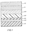
- FIG. 1 shows a cross-section of a typical OLED device in which this invention may be used.
- the invention is as summarized above.
- An OLED device of the invention is a multilayer electroluminescent device comprising a cathode, an anode, charge-injecting layers (if necessary), charge-transporting layers, and a light-emitting layer (LEL) comprising a host and at least one dopant, an indeno[1,2,3- cd ]perylene.
- LEL light-emitting layer
- indenoperylene refers to a perylene core with an indene fusion between the 1,2,3 positions of indene and cd faces of perylene.
- indenoperylene is also used to more generally describe materials wherein the fusion between indene's 1,2,3 positions and perylene's cd faces is not limited solely to indene as defined by the above reference.
- indene can also include analogous materials wherein the benzo-group of indene can be a ring of 5, 6, or 7 atoms comprising carbon or heteroatoms such as nitrogen, sulfur or oxygen.
- the light-emitting layer of the device comprises a host and an emitting dopant where the dopant is present in an amount of up to 10 wt % of the host, more typically from 0.1-2.0 wt % of the host.
- the host functions as an initial "energy capture agent" that transfers that energy to the dopant or guest material as the primary light emitter.
- the host is present in the light emitting layer in an amount of at least 40 wt%.
- Desirable hosts include those based on a chelated oxinoid compound, a benzazole or an anthracene compound although they are not limited to these three classes of host.
- Particular examples of hosts are tris(8-quinolinolato)aluminum (III), 2,2',2"-(1,3,5-benzenetriyl)tris[1-phenyl-lH-benzimidazole] and 2- tert -butyl-9,10-di-(2-naphthyl)anthracene.
- Embodiments of the dopants useful in the invention provide an emitted light having a green hue. Substituents are selected to provide embodiments that exhibit a reduced loss of initial luminance compared to the device containing no indenoperylene of claim 1.
- a useful and convenient embodiment is where R1-10 are all hydrogen and A is a six membered aromatic hydrocarbon ring and two substituents Y are phenyl groups and two other Ys join to form a fused ring.
- a related embodiment is when there are no phenyl groups.
- R1-R10 are selected independently from the group consisting of hydrogen, alkyl and aryl.
- two substituents are selected from R1-10 join to form a fused ring.
- Another useful embodiment is when the atoms comprising X are independently selected as either carbon and/or a heteroatom and which serves to complete a 5 membered ring.
- the emission wavelength of these compounds may be adjusted to some extent by appropriate substitution around the central perylene core.
- the indeno[1,2,3- cd ]perylene compound is usually doped into a host compound, which represents the light-emitting layer between the hole-transporting and electron-transporting layers.
- the host is chosen such that there is efficient energy transfer from the host to the indeno[1,2,3- cd ]perylene compound.
- the indeno[1,2,3- cd ]perylene emits from the excited state to afford a bright, highly-efficient, stable EL device.
- the EL device of the invention is useful in any device where stable light emission is desired such as a lamp or a component in a static or motion imaging device, such as a television, cell phone, DVD player, or computer monitor.
- indeno[1,2,3- cd ]perylene compounds useful in the present invention are the following:
- Embodiments of the invention provide not only improved luminance efficiency but also improved stability under load and typically a more desirable green hue.
- substituted or “substituent” means any group or atom other than hydrogen (what about deuterium).
- group when the term “group” is used, it means that when a substituent group contains a substitutable hydrogen, it is also intended to encompass not only the substituent's unsubstituted form, but also its form further substituted with any substituent group or groups as herein mentioned, so long as the substituent does not destroy properties necessary for device utility.
- a substituent group may be halogen or may be bonded to the remainder of the molecule by an atom of carbon, silicon, oxygen, nitrogen, phosphorous, sulfur, selenium, or boron.
- the substituent may be, for example, halogen, such as chloro, bromo or fluoro; nitro; hydroxyl; cyano; carboxyl; or groups which may be further substituted, such as alkyl, including straight or branched chain or cyclic alkyl, such as methyl, trifluoromethyl, ethyl, t -butyl, 3-(2,4-di- t -pentylphenoxy) propyl, and tetradecyl; alkenyl, such as ethylene, 2-butene; alkoxy, such as methoxy, ethoxy, propoxy, butoxy, 2-methoxyethoxy, sec -butoxy, hexyloxy, 2-ethylhexyloxy, tetradecyloxy, 2-(2,4-di- t -pentylphenoxy)ethoxy, and 2-dodecyloxyethoxy; aryl such as phenyl, 4- t
- the substituents may themselves be further substituted one or more times with the described substituent groups.
- the particular substituents used may be selected by those skilled in the art to attain desirable properties for a specific application and can include, for example, electron-withdrawing groups, electron-donating groups, and steric groups.
- the substituents may be joined together to form a ring such as a fused ring unless otherwise provided.
- the above groups and substituents thereof may include those having up to 48 carbon atoms, typically 1 to 36 carbon atoms and usually less than 24 carbon atoms, but greater numbers are possible depending on the particular substituents selected.
- the present invention can be employed in most OLED device configurations. These include very simple structures comprising a single anode and cathode to more complex devices, such as passive matrix displays comprised of orthogonal arrays of anodes and cathodes to form pixels, and active-matrix displays where each pixel is controlled independently, for example, with a thin film transistor (TFT).
- TFT thin film transistor
- FIG. 1 A more typical structure is shown in Figure 1 and contains a substrate 101 , an anode 103 , an optional hole-injecting layer 105, a hole-transporting layer 107 , a light-emitting layer 109 , an electron-transporting layer 111 , and a cathode 113 . These layers are described in detail below. Note that the substrate may alternatively be located adjacent to the cathode, or the substrate may actually constitute the anode or cathode. Also, the total combined thickness of the organic layers is preferably less than 500 nm.
- the substrate 101 can either be light transmissive or opaque, depending on the intended direction of light emission.
- the light transmissive property is desirable for viewing the EL emission through the substrate.
- Transparent glass or organic material are commonly employed in such cases.
- the transmissive characteristic of the bottom support is immaterial, and therefore can be light transmissive, light absorbing or light reflective.
- Substrates for use in this case include, but are not limited to, glass, plastic, semiconductor materials, ceramics, and circuit board materials. Of course it is necessary to provide in these device configurations a light-transparent top electrode.
- the conductive anode layer 103 is commonly formed over the substrate and, when EL emission is viewed through the anode, should be transparent or substantially transparent to the emission of interest.
- Common transparent anode materials used in this invention are indium-tin oxide (ITO) and tin oxide, but other metal oxides can work including, but not limited to, aluminum- or indium-doped zinc oxide (IZO), magnesium-indium oxide, and nickel-tungsten oxide.
- ITO indium-tin oxide
- IZO aluminum- or indium-doped zinc oxide
- IZO aluminum- or indium-doped zinc oxide
- nickel-tungsten oxide nickel-tungsten oxide.
- metal nitrides such as gallium nitride
- metal selenides such as zinc selenide
- metal sulfides such as zinc sulfide
- the transmissive characteristics of layer 103 are immaterial and any conductive material can be used, transparent, opaque or reflective.
- Example conductors for this application include, but are not limited to, gold, iridium, molybdenum, palladium, and platinum.
- Typical anode materials, transmissive or otherwise, have a work function of 4.1 eV or greater. Desired anode materials are commonly deposited by any suitable means such as evaporation, sputtering, chemical vapor deposition, or electrochemical means. Anodes can be patterned using well-known photolithographic processes.
- HIL Hole-Injecting Layer
- a hole-injecting layer 105 be provided between anode 103 and hole-transporting layer 107 .
- the hole-injecting material can serve to improve the film formation property of subsequent organic layers and to facilitate injection of holes into the hole-transporting layer.
- Suitable materials for use in the hole-injecting layer include, but are not limited to, porphyrinic compounds such as those described in US 4,720,432, and plasma-deposited fluorocarbon polymers such as those described in US 6,208,075.
- Alternative hole-injecting materials reportedly useful in organic EL devices are described in EP 0 891 121 A1 and EP 1 029 909 A1.
- HTL Hole-Transporting Layer
- the hole-transporting layer 107 of the organic EL device contains at least one hole-transporting compound such as an aromatic tertiary amine, where the latter is understood to be a compound containing at least one trivalent nitrogen atom that is bonded only to carbon atoms, at least one of which is a member of an aromatic ring.
- the aromatic tertiary amine can be an arylamine, such as a monoarylamine, diarylamine, triarylamine, or a polymeric arylamine group. Exemplary monomeric triarylamines are illustrated by Klupfel et al. US 3,180,730.
- Other suitable triarylamines substituted with one or more vinyl radicals and/or comprising at least one active hydrogen containing group are disclosed by Brantley et al US 3,567,450 and US 3,658,520.
- a more preferred class of aromatic tertiary amines are those which include at least two aromatic tertiary amine moieties as described in US 4,720,432 and US 5,061,569.
- Such compounds include those represented by structural formula (A). wherein Q 1 and Q 2 are independently selected aromatic tertiary amine moieties and G is a linking group such as an arylene, cycloalkylene, or alkylene group of a carbon to carbon bond.
- at least one of Q 1 or Q 2 contains a polycyclic fused ring group, e.g., a naphthalene.
- G is an aryl group, it is conveniently a phenylene, biphenylene, or naphthalene group.
- a useful class of triarylamine groups satisfying structural formula (A) and containing two triarylamine groups is represented by structural formula (B): where R 1 and R 2 each independently represents a hydrogen atom, an aryl group, or an alkyl group or R 1 and R 2 together represent the atoms completing a cycloalkyl group; and R 3 and R 4 each independently represents an aryl group, which is in turn substituted with a diaryl substituted amino group, as indicated by structural formula (C): wherein R 5 and R 6 are independently selected aryl groups.
- at least one of R 5 or R 6 contains a polycyclic fused ring group, e.g., a naphthalene.
- tetraaryldiamines Another class of aromatic tertiary amine groups are the tetraaryldiamines. Desirable tetraaryldiamines groups include two diarylamino groups, such as indicated by formula (C), linked through an arylene group. Useful tetraaryldiamines include those represented by formula (D). wherein each Are is an independently selected arylene group, such as a phenylene or anthracene group, n is an integer of from 1 to 4, and Ar, R 7 , R 8 , and R 9 are independently selected aryl groups. In a typical embodiment, at least one of Ar, R 7 , R 8 , and R 9 is a polycyclic fused ring group, e.g., a naphthalene
- the various alkyl, alkylene, aryl, and arylene groups of the foregoing structural formulae (A), (B), (C), (D), can each in turn be substituted.
- Typical substituents include alkyl groups, alkoxy groups, aryl groups, aryloxy groups, and halogen such as fluoride, chloride, and bromide.
- the various alkyl and alkylene groups typically contain from 1 to 6 carbon atoms.
- the cycloalkyl moieties can contain from 3 to 10 carbon atoms, but typically contain five, six, or seven ring carbon atoms--e.g., cyclopentyl, cyclohexyl, and cycloheptyl ring structures.
- the aryl and arylene groups are usually phenyl and phenylene moieties.
- the hole-transporting layer can be formed of a single or a mixture of aromatic tertiary amine compounds.
- a triarylamine such as a triarylamine satisfying the formula (B)
- a tetraaryldiamine such as indicated by formula (D).
- a triarylamine is employed in combination with a tetraaryldiamine, the latter is positioned as a layer interposed between the triarylamine and the electron injecting and transporting layer.
- useful aromatic tertiary amines are the following:
- Another class of useful hole-transporting materials includes polycyclic aromatic compounds as described in EP 1 009 041.
- polymeric hole-transporting materials can be used such as poly( N -vinylcarbazole) (PVK), polythiophenes, polypyrrole, polyaniline, and copolymers such as poly(3,4-ethylenedioxythiophene) / poly(4-styrenesulfonate) also called PEDOT/PSS.
- the light-emitting layer (LEL) 109 of the organic EL element comprises a luminescent or fluorescent material where electroluminescence is produced as a result of electron-hole pair recombination in this region.
- the light-emitting layer can be comprised of a single material, but more commonly consists of a host material doped with a guest compound or compounds where light emission comes primarily from the dopant and can be of any color.
- the host materials in the light-emitting layer can be an electron-transporting material, as defined below, a hole-transporting material, as defined above, or another material or combination of materials that support hole-electron recombination.
- the dopant is usually chosen from highly fluorescent dyes, but phosphorescent compounds, e.g., transition metal complexes as described in WO 98/55561, WO 00/18851, WO 00/57676, and WO 00/70655 are also useful. Dopants are typically coated as 0.01 to 10 % by weight into the host material.
- Host and emitting molecules known to be of use include, but are not limited to, those disclosed in US 4,768,292, US 5,141,671, US 5,150,006, US 5,151,629, US 5,405,709, US 5,484,922, US 5,593,788, US 5,645,948, US 5,683,823, US 5,755,999, US 5,928,802, US 5,935,720, US 5,935,721, and US 6,020,078.
- Form E Metal complexes of 8-hydroxyquinoline and similar derivatives constitute one class of useful host compounds capable of supporting electroluminescence, and are particularly suitable for light emission of wavelengths longer than 500 nm, e.g., green, yellow, orange, and red.
- the metal can be monovalent, divalent, trivalent, or tetravalent metal.
- the metal can, for example, be an alkali metal, such as lithium, sodium, or potassium; an alkaline earth metal, such as magnesium or calcium; an earth metal, such aluminum or gallium, or a transition metal such as zinc or zirconium.
- alkali metal such as lithium, sodium, or potassium
- alkaline earth metal such as magnesium or calcium
- earth metal such aluminum or gallium, or a transition metal such as zinc or zirconium.
- any monovalent, divalent, trivalent, or tetravalent metal known to be a useful chelating metal can be employed.
- Z completes a heterocyclic nucleus containing at least two fused aromatic rings, at least one of which is an azole or azine ring. Additional rings, including both aliphatic and aromatic rings, can be fused with the two required rings, if required. To avoid adding molecular bulk without improving on function the number of ring atoms is usually maintained at 18 or less.
- Illustrative of useful chelated oxinoid compounds are the following:
- Formula F Derivatives of 9,10-di-(2-naphthyl)anthracene (Formula F) constitute one class of useful hosts capable of supporting electroluminescence, and are particularly suitable for light emission of wavelengths longer than 400 nm, e.g., blue, green, yellow, orange or red.
- R 1 , R 2 , R 3 , R 4 , R 5 , and R 6 represent hydrogen or one or more substituents selected from the following groups:
- Illustrative examples include 9,10-di-(2-naphthyl)anthracene and 2- t -butyl-9,10-di-(2-naphthyl)anthracene.
- Other anthracene derivatives can be useful as a host in the LEL, including derivatives of 9,10-bis[4-(2,2-diphenylethenyl)phenyl]anthracene, and phenylanthracene derivatives as described in EP 681,019.
- Benzazole derivatives constitute another class of useful hosts capable of supporting electroluminescence, and are particularly suitable for light emission of wavelengths longer than 400 nm, e.g., blue, green, yellow, orange or red.
- An example of a useful benzazole is 2, 2', 2"-(1,3,5-phenylene)tris[1-phenyl-1H-benzimidazole], (TPBI).
- Distyrylarylene derivatives as described in US 5,121,029 are also useful host materials in the LEL.
- Desirable fluorescent dopants include groups derived from fused ring, heterocyclic and other compounds such as anthracene, tetracene, xanthene, perylene, rubrene, coumarin, rhodamine, quinacridone, dicyanomethylenepyran, thiopyran, polymethine, pyrilium thiapyrilium, and carbostyryl compounds.
- useful dopants include, but are not limited to, the following:
- ETL Electron-Transporting Layer
- Preferred thin film-forming materials for use in forming the electron-transporting layer 111 of the organic EL devices of this invention are metal chelated oxinoid compounds, including chelates of oxine itself (also commonly referred to as 8-quinolinol or 8-hydroxyquinoline). Such compounds help to inject and transport electrons and exhibit both high levels of performance and are readily fabricated in the form of thin films.
- exemplary of contemplated oxinoid compounds are those satisfying structural formula (E), previously described.
- electron-transporting materials include various butadiene derivatives as disclosed in US 4,356,429 and various heterocyclic optical brighteners as described in US 4,539,507. Benzazoles satisfying structural formula (G) are also useful electron transporting materials.
- layers 109 and 111 can optionally be collapsed into a single layer that serves the function of supporting both light emission and electron transportation.
- the cathode layer 113 used in this invention can be comprised of nearly any conductive material. Desirable materials have good film-forming properties to ensure good contact with the underlying organic layer, promote electron injection at low voltage, and have good stability. Useful cathode materials often contain a low work function metal ( ⁇ 4.0 eV) or metal alloy.
- a low work function metal ⁇ 4.0 eV
- One preferred cathode material is comprised of a Mg:Ag alloy wherein the percentage of silver is in the range of 1 to 20 %, as described in US 4,885,221.
- Another suitable class of cathode materials includes bilayers comprised of a thin layer of a low work function metal or metal salt capped with a thicker layer of conductive metal.
- cathode is comprised of a thin layer of LiF followed by a thicker layer of Al as described in US 5,677,572.
- Other useful cathode materials include, but are not limited to, those disclosed in US 5,059,861, US 5,059,862, and US 6,140,763.
- cathode When light emission is viewed through the cathode, the cathode must be transparent or nearly transparent. For such applications, metals must be thin or one must use transparent conductive oxides, or a combination of these materials.
- Optically transparent cathodes have been described in more detail in US 5,776,623. Cathode materials can be deposited by evaporation, sputtering, or chemical vapor deposition. When needed, patterning can be achieved through many well known methods including, but not limited to, through-mask deposition, integral shadow masking as described in US 5,276,380 and EP 0 732 868, laser ablation, and selective chemical vapor deposition.
- the organic materials mentioned above are suitably deposited through sublimation, but can be deposited from a solvent with an optional binder to improve film formation. If the material is a polymer, solvent deposition is usually preferred.
- the material to be deposited by sublimation can be vaporized from a sublimator "boat" often comprised of a tantalum material, e.g., as described in US 6,237,529, or can be first coated onto a donor sheet and then sublimed in closer proximity to the substrate. Layers with a mixture of materials can utilize separate sublimator boats or the materials can be pre-mixed and coated from a single boat or donor sheet.
- Patterned deposition can be achieved using shadow masks, integral shadow masks (US 5,294,870), spatially-defined thermal dye transfer from a donor sheet (US 5,851,709 and US 6,066,357) and inkjet method (US 6,066,357).
- OLED devices are sensitive to moisture and/or oxygen so they are commonly sealed in an inert atmosphere such as nitrogen or argon, along with a desiccant such as alumina, bauxite, calcium sulfate, clays, silica gel, zeolites, alkaline metal oxides, alkaline earth metal oxides, sulfates, or metal halides and perchlorates.
- a desiccant such as alumina, bauxite, calcium sulfate, clays, silica gel, zeolites, alkaline metal oxides, alkaline earth metal oxides, sulfates, or metal halides and perchlorates.
- OLED devices require a Hole-Blocking Layer to either facilitate injection of electrons into the LEL or attenuate the passage of holes into the ETL to ensure recombination in the LEL (D. F. O'brien, M. A. Baldo, M. E. Thompson, and S. R. Forrest Appl. Phys. Lett. 74, 442 (1999)).
- this layer is thin (i.e., 10 nm) and it is located between the LEL and ETL.
- Example 1 - EL Device Fabrication - Inventive Example
- a glass substrate coated with an 85 nm layer of indium-tin oxide (ITO) as the anode was sequentially ultrasonicated in a commercial detergent, rinsed in deionized water, degreased in toluene vapor and exposed to oxygen plasma for about 1 min.
- ITO indium-tin oxide
- the above sequence completed the deposition of the EL device.
- the device was then hermetically packaged in a dry glove box for protection against ambient environment.
- Table 1 summarizes data for use of Inv-1 in an OLED.
- the "sample” column lists the six devices that were simultaneously prepared.
- the “type” column describes cells as having used the invention or as a comparison, check, cells.
- the “Inv-1” column lists the amount of dopant deposited in each cell.
- the “efficiency” column is a measure of the ability of a given device to convert a charge recombination into light emission as measured in units of candella per ampere(cd/A).
- the luminance column (L) reflects the light output of a cell (cd/m 2 ) for a given unit of area.
- the "T 50 " column lists the time required at elevated temperature for a device to lose 50% luminance while operating at a constant current of 20 mA/cm 2 .
- L t L 0 exp(A t B ), where L t is luminance at time t, L 0 is initial luminance, A and B are empirical fit parameters, found to be -0.00969 and 0.59, respectively.
- a glass substrate coated with an 85 nm layer of indium-tin oxide (ITO) as the anode was sequentially ultrasonicated in a commercial detergent, rinsed in deionized water, degreased in toluene vapor and exposed to oxygen plasma for about 1 min.
- ITO indium-tin oxide
- the above sequence completed the deposition of the EL device.
- the device was then hermetically packaged in a dry glove box for protection against ambient environment.
- the tested EL device incorporating the Inv-1 dopant in a TBADN host demonstrates a superior luminance yield relative to the comparative device.
- the inventive device exhibited green emission ( ⁇ max of 544 nm) with a well-defined vibronic structure and narrow emission peaks as opposed to the very blue TBADN emission at 448 nm.
- a glass substrate coated with an 85 nm layer of indium-tin oxide (ITO) as the anode was sequentially ultrasonicated in a commercial detergent, rinsed in deionized water, degreased in toluene vapor and exposed to oxygen plasma for about 1 min.
- ITO indium-tin oxide
- the above sequence completed the deposition of the EL device.
- the device was then hermetically packaged in a dry glove box for protection against ambient environment.
- the tested EL device incorporating the Inv-1 dopant in a TBADN host demonstrates a superior luminance yield relative to the comparative device.
- the inventive device exhibited green emission ( ⁇ max of 540 nm) with a well-defined vibronic structure and narrow emission peaks as opposed to the very blue TBADN emission at 452 nm.
- Comp-1 The reported luminance yields for Comp-1 are similar to those of the inventive examples tested. However, in general the quinacridone green dopants exhibit a decreased operational stability relative to inventive examples.
- a typical device is detailed in Table 4 wherein Comp-1 (3,10-difluoro-5,12-dimethyl-7,14-dione-quino[2,3-b]acridine) is employed as a typical illustration of quinacridone-green-dopant performance.
- the invention includes a device of the invention where the TBADN has the formula: the host (Alq 3 ) has the formula: the host is present in the light emitting layer in an amount of at least 40 wt%; the substituents and the ring size of A are selected so as to provide luminescence stability improvements for aged devices; the substituents of the indenoperylene are selected to provide improved luminescence efficiency compared to the device with no indenoperylene dopant; ring A contains Y substituents joined to form more than one fused ring; at least one of Y is independently selected from the group consisting of halide, alkyl, aryl, alkoxy, and aryloxy; R1-10 are hydrogen; two of R1, R2, R3, R4, R5, R6, R7, R8, R9, and R10 join to form a fused ring; at least one of R1, R2, R3, R4, R5, R6, R7, R8, R9, and R10 are independently selected from the group consisting of halide
Landscapes
- Physics & Mathematics (AREA)
- Spectroscopy & Molecular Physics (AREA)
- Chemical & Material Sciences (AREA)
- Engineering & Computer Science (AREA)
- Materials Engineering (AREA)
- Electroluminescent Light Sources (AREA)
- Organic Low-Molecular-Weight Compounds And Preparation Thereof (AREA)
Abstract
Description
- This invention relates to an organic light emitting diode (OLED) electroluminescent (EL) device comprising a light-emitting layer containing an indeno[1,2,3-cd]perylene compound.
- While organic electroluminescent (EL) devices have been known for over two decades, their performance limitations have represented a barrier to many desirable applications. In simplest form, an organic EL device is comprised of an anode for hole injection, a cathode for electron injection, and an organic medium sandwiched between these electrodes to support charge recombination that yields emission of light. These devices are also commonly referred to as organic light-emitting diodes, or OLEDs. Representative of earlier organic EL devices are Gurnee et al. U.S. Pat. No. 3,172,862, issued Mar. 9, 1965; Gurnee U.S. Pat. No. 3,173,050, issued Mar. 9, 1965; Dresner, "Double Injection Electroluminescence in Anthracene", RCA Review, Vol. 30, pp. 322-334, 1969; and Dresner U.S. Pat. No. 3,710,167, issued Jan. 9, 1973. The organic layers in these devices, usually composed of a polycyclic aromatic hydrocarbon, were very thick (much greater than 1 µm). Consequently, operating voltages were very high, often >100V.
- More recent organic EL devices include an organic EL element consisting of extremely thin layers (e.g. <1.0 µm ) between the anode and the cathode. Herein, the organic EL element encompasses the layers between the anode and cathode electrodes. Reducing the thickness lowered the resistance of the organic layer and has enabled devices that operate at much lower voltage. In a basic two-layer EL device structure, described first in US 4,356,429, one organic layer of the EL element adjacent to the anode is specifically chosen to transport holes, therefore, it is referred to as the hole-transporting layer, and the other organic layer is specifically chosen to transport electrons, referred to as the electron-transporting layer. The interface between the two layers provides an efficient site for the recombination of the injected hole/electron pair and the resultant electroluminescence.
- There have also been proposed three-layer organic EL devices that contain an organic light-emitting layer (LEL) between the hole- transporting layer and electron-transporting layer, such as that disclosed by Tang et al [J. Applied Physics, Vol. 65, Pages 3610-3616, 1989]. The light-emitting layer commonly consists of a host material doped with a guest material - dopant , which results in an efficiency improvement and allows color tuning.
- Since these early inventions, further improvements in device materials have resulted in improved performance in attributes such as color, stability, luminance efficiency and manufacturability, e.g., as disclosed in US 5,061,569, US 5,409,783, US 5,554,450, US 5,593,788, US 5,683,823, US 5, 908,581, US 5,928,802, US 6,020,078, and US 6,208,077, amongst others.
- Notwithstanding these developments, there are continuing needs for organic EL device components, such as dopants, that will provide high luminance efficiencies combined with high color purity and long lifetimes.
- A useful class of dopants is derived from the quinacridone compounds and disclosed in US 5,593,788. These materials are characterized by a broad emission envelope and a high luminance quantum yield. However, the stability of these materials in an OLED is insufficient for a broad range of OLED applications.
- Another useful class of dopants is the indenoperylene class of materials as disclosed in EP 1 148 109 A2. These materials are characterized by a "perylene-type" emission spectrum in the green region of the spectrum. It is reported in this work that materials of this class provide unexpected and exceptional device stability when used as a dopant in anthracene and oxinoid hosts as a dopant.
- It is a problem to be solved to provide a dopant compound for a light-emitting layer of an OLED device that exhibits improved luminance stability improved luminance efficiency.
- The invention provides an OLED device comprising an anode, a hole transporting layer (HTL), a green light emitting layer (LEL), an electron transporting layer (ETL) and a cathode wherein the light emitting layer comprises a host and up to 10 wt% of a green light emitting indeno[1,2,3-cd]perylene dopant compound.
- Devices of the invention provide improved luminance efficiency.
- FIG. 1 shows a cross-section of a typical OLED device in which this invention may be used.
- The invention is as summarized above.
- An OLED device of the invention is a multilayer electroluminescent device comprising a cathode, an anode, charge-injecting layers (if necessary), charge-transporting layers, and a light-emitting layer (LEL) comprising a host and at least one dopant, an indeno[1,2,3-cd]perylene. The term indenoperylene refers to a perylene core with an indene fusion between the 1,2,3 positions of indene and cd faces of perylene. [See The Naming and Indexing of Chemical Substances for Chemical Abstracts-A Reprint of Index IV (Chemical Substance Index Names) from the Chemical Abstracts - 1992 Index Guide; American Chemical Society: Columbus, OH, 1992; paragraph 135,148 and 150. Debad, J. D.; Morris, J. C.; Lynch, V.; Magnus, P.; Bard, A. J. Am. Chem. Soc. 1996, 118, 2374-2379]. In this specification, the term indenoperylene is also used to more generally describe materials wherein the fusion between indene's 1,2,3 positions and perylene's cd faces is not limited solely to indene as defined by the above reference. In this case indene can also include analogous materials wherein the benzo-group of indene can be a ring of 5, 6, or 7 atoms comprising carbon or heteroatoms such as nitrogen, sulfur or oxygen.
- Suitably, the light-emitting layer of the device comprises a host and an emitting dopant where the dopant is present in an amount of up to 10 wt % of the host, more typically from 0.1-2.0 wt % of the host. The host functions as an initial "energy capture agent" that transfers that energy to the dopant or guest material as the primary light emitter. The host is present in the light emitting layer in an amount of at least 40 wt%.
- The benefit imparted by the dopant does not appear to be host specific. Desirable hosts include those based on a chelated oxinoid compound, a benzazole or an anthracene compound although they are not limited to these three classes of host. Particular examples of hosts are tris(8-quinolinolato)aluminum (III), 2,2',2"-(1,3,5-benzenetriyl)tris[1-phenyl-lH-benzimidazole] and 2-tert-butyl-9,10-di-(2-naphthyl)anthracene.
- Embodiments of the dopants useful in the invention provide an emitted light having a green hue. Substituents are selected to provide embodiments that exhibit a reduced loss of initial luminance compared to the device containing no indenoperylene of claim 1.
- Compounds useful in the invention are suitably represented by Formula (1):wherein

- A represents an independent ring system in which X represents a chain of a combined total of "n" carbon or heteroatoms which serve to complete a 5, 6 or 7 membered ring;
- each Y is an independently selected substituent, two of which may join to form a fused ring to A;
- m is 0 to 5; and
- R1, R2, R3, R4, R5, R6, R7, R8, R9, and R10 are independently selected as hydrogen or substituents;
- provided that any of the indicated substituents may join to form further fused rings.
-
- A useful and convenient embodiment is where R1-10 are all hydrogen and A is a six membered aromatic hydrocarbon ring and two substituents Y are phenyl groups and two other Ys join to form a fused ring. A related embodiment is when there are no phenyl groups. Another desirable embodiment is where R1-R10 are selected independently from the group consisting of hydrogen, alkyl and aryl. In one useful embodiment, two substituents are selected from R1-10 join to form a fused ring. Another useful embodiment is when the atoms comprising X are independently selected as either carbon and/or a heteroatom and which serves to complete a 5 membered ring.
- The emission wavelength of these compounds may be adjusted to some extent by appropriate substitution around the central perylene core.

- The indeno[1,2,3-cd]perylene compound is usually doped into a host compound, which represents the light-emitting layer between the hole-transporting and electron-transporting layers. The host is chosen such that there is efficient energy transfer from the host to the indeno[1,2,3-cd]perylene compound. The indeno[1,2,3-cd]perylene emits from the excited state to afford a bright, highly-efficient, stable EL device.
- The EL device of the invention is useful in any device where stable light emission is desired such as a lamp or a component in a static or motion imaging device, such as a television, cell phone, DVD player, or computer monitor.
- Illustrative examples of indeno[1,2,3-cd]perylene compounds useful in the present invention are the following:


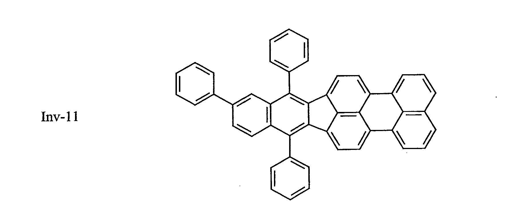


- Embodiments of the invention provide not only improved luminance efficiency but also improved stability under load and typically a more desirable green hue.
- Unless otherwise specifically stated, use of the term "substituted" or "substituent" means any group or atom other than hydrogen (what about deuterium). Additionally, when the term "group" is used, it means that when a substituent group contains a substitutable hydrogen, it is also intended to encompass not only the substituent's unsubstituted form, but also its form further substituted with any substituent group or groups as herein mentioned, so long as the substituent does not destroy properties necessary for device utility. Suitably, a substituent group may be halogen or may be bonded to the remainder of the molecule by an atom of carbon, silicon, oxygen, nitrogen, phosphorous, sulfur, selenium, or boron. The substituent may be, for example, halogen, such as chloro, bromo or fluoro; nitro; hydroxyl; cyano; carboxyl; or groups which may be further substituted, such as alkyl, including straight or branched chain or cyclic alkyl, such as methyl, trifluoromethyl, ethyl, t-butyl, 3-(2,4-di-t-pentylphenoxy) propyl, and tetradecyl; alkenyl, such as ethylene, 2-butene; alkoxy, such as methoxy, ethoxy, propoxy, butoxy, 2-methoxyethoxy, sec-butoxy, hexyloxy, 2-ethylhexyloxy, tetradecyloxy, 2-(2,4-di-t-pentylphenoxy)ethoxy, and 2-dodecyloxyethoxy; aryl such as phenyl, 4-t-butylphenyl, 2,4,6-trimethylphenyl, naphthyl; aryloxy, such as phenoxy, 2-methylphenoxy, alpha- or beta-naphthyloxy, and 4-tolyloxy; carbonamido, such as acetamido, benzamido, butyramido, tetradecanamido, alpha-(2,4-di-t-pentyl-phenoxy)acetamido, alpha-(2,4-di-t-pentylphenoxy)butyramido, alpha-(3-pentadecylphenoxy)-hexanamido, alpha-(4-hydroxy-3-t-butylphenoxy)-tetradecanamido, 2-oxo-pyrrolidin-1-yl, 2-oxo-5-tetradecylpyrrolin-1-yl, N-methyltetradecanamido, N-succinimido, N-phthalimido, 2,5-dioxo-1-oxazolidinyl, 3-dodecyl-2,5-dioxo-1-imidazolyl, and N-acetyl-N-dodecylamino, ethoxycarbonylamino, phenoxycarbonylamino, benzyloxycarbonylamino, hexadecyloxycarbonylamino, 2,4-di-t-butylphenoxycarbonylamino, phenylcarbonylamino, 2,5-(di-t-pentylphenyl)carbonylamino, p-dodecyl-phenylcarbonylamino, p-tolylcarbonylamino, N-methylureido, N,N-dimethylureido, N-methyl-N-dodecylureido, N-hexadecylureido, N,N-dioctadecylureido, N,N-dioctyl-N'-ethylureido, N-phenylureido, N,N-diphenylureido, N-phenyl-N-p-tolylureido, N-(m-hexadecylphenyl)ureido, N,N-(2,5-di-t-pentylphenyl)-N'-ethylureido, and t-butylcarbonamido; sulfonamido, such as methylsulfonamido, benzenesulfonamido, p-tolylsulfonamido, p-dodecylbenzenesulfonamido, N-methyltetradecylsulfonamido, N,N-dipropyl-sulfamoylamino, and hexadecylsulfonamido; sulfamoyl, such as N-methylsulfamoyl, N-ethylsulfamoyl, N,N-dipropylsulfamoyl, N-hexadecylsulfamoyl, N,N-dimethylsulfamoyl, N-[3-(dodecyloxy)propyl]sulfamoyl, N-[4-(2,4-di-t-pentylphenoxy)butyl]sulfamoyl, N-methyl-N-tetradecylsulfamoyl, and N-dodecylsulfamoyl; carbamoyl, such as N-methylcarbamoyl, N,N-dibutylcarbamoyl, N-octadecylcarbamoyl, N-[4-(2,4-di-t-pentylphenoxy)butyl] carbamoyl, N-methyl-N-tetradecylcarbamoyl, and N,N-dioctylcarbamoyl; acyl, such as acetyl, (2,4-di-t-amylphenoxy)acetyl, phenoxycarbonyl, p-dodecyloxyphenoxycarbonyl methoxycarbonyl, butoxycarbonyl, tetradecyloxycarbonyl, ethoxycarbonyl, benzyloxycarbonyl, 3-pentadecyloxycarbonyl, and dodecyloxycarbonyl; sulfonyl, such as methoxysulfonyl, octyloxysulfonyl, tetradecyloxysulfonyl, 2-ethylhexyloxysulfonyl, phenoxysulfonyl, 2,4-di-t-pentylphenoxysulfonyl, methylsulfonyl, octylsulfonyl, 2-ethylhexylsulfonyl, dodecylsulfonyl, hexadecylsulfonyl, phenylsulfonyl, 4-nonylphenylsulfonyl, and p-tolylsulfonyl; sulfonyloxy, such as dodecylsulfonyloxy, and hexadecylsulfonyloxy; sulfinyl, such as methylsulfinyl, octylsulfinyl, 2-ethylhexylsulfinyl, dodecylsulfinyl, hexadecylsulfinyl, phenylsulfinyl, 4-nonylphenylsulfinyl, and p-tolylsulfinyl; thio, such as ethylthio, octylthio, benzylthio, tetradecylthio, 2-(2,4-di-t-pentylphenoxy)ethylthio, phenylthio, 2-butoxy-5-t-octylphenylthio, and p-tolylthio; acyloxy, such as acetyloxy, benzoyloxy, octadecanoyloxy, p-dodecylamidobenzoyloxy, N-phenylcarbamoyloxy, N-ethylcarbamoyloxy, and cyclohexylcarbonyloxy; amine, such as phenylanilino, 2-chloroanilino, diethylamine, dodecylamine; imino, such as 1 (N-phenylimido)ethyl, N-succinimido or 3-benzylhydantoinyl; phosphate, such as dimethylphosphate and ethylbutylphosphate; phosphite, such as diethyl and dihexylphosphite; a heterocyclic group, a heterocyclic oxy group or a heterocyclic thio group, each of which may be substituted and which contain a 3 to 7 membered heterocyclic ring composed of carbon atoms and at least one hetero atom selected from the group consisting of oxygen, nitrogen, sulfur, phosphorous, or boron. Such as 2-furyl, 2-thienyl, 2-benzimidazolyloxy or 2-benzothiazolyl; quaternary ammonium, such as triethylammonium; quaternary phosphonium, such as triphenylphosphonium; and silyloxy, such as trimethylsilyloxy.
- If desired, the substituents may themselves be further substituted one or more times with the described substituent groups. The particular substituents used may be selected by those skilled in the art to attain desirable properties for a specific application and can include, for example, electron-withdrawing groups, electron-donating groups, and steric groups. When a molecule may have two or more substituents, the substituents may be joined together to form a ring such as a fused ring unless otherwise provided. Generally, the above groups and substituents thereof may include those having up to 48 carbon atoms, typically 1 to 36 carbon atoms and usually less than 24 carbon atoms, but greater numbers are possible depending on the particular substituents selected.
- The present invention can be employed in most OLED device configurations. These include very simple structures comprising a single anode and cathode to more complex devices, such as passive matrix displays comprised of orthogonal arrays of anodes and cathodes to form pixels, and active-matrix displays where each pixel is controlled independently, for example, with a thin film transistor (TFT).
- There are numerous configurations of the organic layers wherein the present invention can be successfully practiced. Essential requirements are a cathode, an anode, an HTL and an LEL. A more typical structure is shown in Figure 1 and contains a
substrate 101, ananode 103, an optional hole-injectinglayer 105, a hole-transportinglayer 107, a light-emittinglayer 109, an electron-transporting layer 111, and acathode 113. These layers are described in detail below. Note that the substrate may alternatively be located adjacent to the cathode, or the substrate may actually constitute the anode or cathode. Also, the total combined thickness of the organic layers is preferably less than 500 nm. - The
substrate 101 can either be light transmissive or opaque, depending on the intended direction of light emission. The light transmissive property is desirable for viewing the EL emission through the substrate. Transparent glass or organic material are commonly employed in such cases. For applications where the EL emission is viewed through the top electrode, the transmissive characteristic of the bottom support is immaterial, and therefore can be light transmissive, light absorbing or light reflective. Substrates for use in this case include, but are not limited to, glass, plastic, semiconductor materials, ceramics, and circuit board materials. Of course it is necessary to provide in these device configurations a light-transparent top electrode. - The
conductive anode layer 103 is commonly formed over the substrate and, when EL emission is viewed through the anode, should be transparent or substantially transparent to the emission of interest. Common transparent anode materials used in this invention are indium-tin oxide (ITO) and tin oxide, but other metal oxides can work including, but not limited to, aluminum- or indium-doped zinc oxide (IZO), magnesium-indium oxide, and nickel-tungsten oxide. In addition to these oxides, metal nitrides, such as gallium nitride, and metal selenides, such as zinc selenide, and metal sulfides, such as zinc sulfide, can be used inlayer 103. For applications where EL emission is viewed through the top electrode, the transmissive characteristics oflayer 103 are immaterial and any conductive material can be used, transparent, opaque or reflective. Example conductors for this application include, but are not limited to, gold, iridium, molybdenum, palladium, and platinum. Typical anode materials, transmissive or otherwise, have a work function of 4.1 eV or greater. Desired anode materials are commonly deposited by any suitable means such as evaporation, sputtering, chemical vapor deposition, or electrochemical means. Anodes can be patterned using well-known photolithographic processes. - While not always necessary, it is often useful that a hole-injecting
layer 105 be provided betweenanode 103 and hole-transportinglayer 107. The hole-injecting material can serve to improve the film formation property of subsequent organic layers and to facilitate injection of holes into the hole-transporting layer. Suitable materials for use in the hole-injecting layer include, but are not limited to, porphyrinic compounds such as those described in US 4,720,432, and plasma-deposited fluorocarbon polymers such as those described in US 6,208,075. Alternative hole-injecting materials reportedly useful in organic EL devices are described in EP 0 891 121 A1 and EP 1 029 909 A1. - The hole-transporting
layer 107 of the organic EL device contains at least one hole-transporting compound such as an aromatic tertiary amine, where the latter is understood to be a compound containing at least one trivalent nitrogen atom that is bonded only to carbon atoms, at least one of which is a member of an aromatic ring. In one form the aromatic tertiary amine can be an arylamine, such as a monoarylamine, diarylamine, triarylamine, or a polymeric arylamine group. Exemplary monomeric triarylamines are illustrated by Klupfel et al. US 3,180,730. Other suitable triarylamines substituted with one or more vinyl radicals and/or comprising at least one active hydrogen containing group are disclosed by Brantley et al US 3,567,450 and US 3,658,520. - A more preferred class of aromatic tertiary amines are those which include at least two aromatic tertiary amine moieties as described in US 4,720,432 and US 5,061,569. Such compounds include those represented by structural formula (A).wherein Q1 and Q2 are independently selected aromatic tertiary amine moieties and G is a linking group such as an arylene, cycloalkylene, or alkylene group of a carbon to carbon bond. In one embodiment, at least one of Q1 or Q2 contains a polycyclic fused ring group, e.g., a naphthalene. When G is an aryl group, it is conveniently a phenylene, biphenylene, or naphthalene group.

- A useful class of triarylamine groups satisfying structural formula (A) and containing two triarylamine groups is represented by structural formula (B):where

R1 and R2 each independently represents a hydrogen atom, an aryl group, or an alkyl group or R1 and R2 together represent the atoms completing a cycloalkyl group; and
R3 and R4 each independently represents an aryl group, which is in turn substituted with a diaryl substituted amino group, as indicated by structural formula (C):wherein R5 and R6 are independently selected aryl groups. In one embodiment, at least one of R5 or R6 contains a polycyclic fused ring group, e.g., a naphthalene.
- Another class of aromatic tertiary amine groups are the tetraaryldiamines. Desirable tetraaryldiamines groups include two diarylamino groups, such as indicated by formula (C), linked through an arylene group. Useful tetraaryldiamines include those represented by formula (D).wherein

each Are is an independently selected arylene group, such as a phenylene or anthracene group,
n is an integer of from 1 to 4, and
Ar, R7, R8, and R9 are independently selected aryl groups.
In a typical embodiment, at least one of Ar, R7, R8, and R9 is a polycyclic fused ring group, e.g., a naphthalene - The various alkyl, alkylene, aryl, and arylene groups of the foregoing structural formulae (A), (B), (C), (D), can each in turn be substituted. Typical substituents include alkyl groups, alkoxy groups, aryl groups, aryloxy groups, and halogen such as fluoride, chloride, and bromide. The various alkyl and alkylene groups typically contain from 1 to 6 carbon atoms. The cycloalkyl moieties can contain from 3 to 10 carbon atoms, but typically contain five, six, or seven ring carbon atoms--e.g., cyclopentyl, cyclohexyl, and cycloheptyl ring structures. The aryl and arylene groups are usually phenyl and phenylene moieties.
- The hole-transporting layer can be formed of a single or a mixture of aromatic tertiary amine compounds. Specifically, one may employ a triarylamine, such as a triarylamine satisfying the formula (B), in combination with a tetraaryldiamine, such as indicated by formula (D). When a triarylamine is employed in combination with a tetraaryldiamine, the latter is positioned as a layer interposed between the triarylamine and the electron injecting and transporting layer. Illustrative of useful aromatic tertiary amines are the following:
- 1,1-Bis(4-di- p -tolylaminophenyl)cyclohexane
- 1,1-Bis(4-di- p -tolylaminophenyl)-4-phenylcyclohexane
- 4,4'-Bis(diphenylamino)quadriphenyl
- Bis(4-dimethylamino-2-methylphenyl)-phenylmethane
- N,N,N-Tri( p -tolyl)amine
- 4-(di-p-tolylamino)-4'-[4(di- p -tolylamino)-styryl]stilbene
- N,N,N',N'-Tetra- p -tolyl-4-4'-diaminobiphenyl
- N,N,N',N'-Tetraphenyl-4,4'-diaminobiphenyl
- N,N,N',N'-tetra-1-naphthyl-4,4'-diaminobiphenyl
- N,N,N',N'-tetra-2-naphthyl-4,4'-diaminobiphenyl
- N-Phenylcarbazole
- 4,4'-Bis[N-(1-naphthyl)-N-phenylamino]biphenyl
- 4,4'-Bis[N-(1-naphthyl)-N-(2-naphthyl)amino]biphenyl
- 4,4"-Bis[N-(1-naphthyl)-N-phenylamino]p-terphenyl
- 4,4'-Bis[N-(2-naphthyl)-N-phenylamino]biphenyl
- 4,4'-Bis[N-(3-acenaphthenyl)-N-phenylamino]biphenyl
- 1,5-Bis[N-(1-naphthyl)-N-phenylamino]naphthalene
- 4,4'-Bis[N-(9-anthryl)-N-phenylamino]biphenyl
- 4,4"-Bis[N-(1-anthryl)-N-phenylamino]-p-terphenyl
- 4,4'-Bis[N-(2-phenanthryl)-N-phenylamino]biphenyl
- 4,4'-Bis[N-(8-fluoranthenyl)-N-phenylamino]biphenyl
- 4,4'-Bis[N-(2-pyrenyl)-N-phenylamino]biphenyl
- 4,4'-Bis[N-(2-naphthacenyl)-N-phenylamino]biphenyl
- 4,4'-Bis[N-(2-perylenyl)-N-phenylamino]biphenyl
- 4,4'-Bis[N-(1-coronenyl)-N-phenylamino]biphenyl
- 2,6-Bis(di- p -tolylamino)naphthalene
- 2,6-Bis[di-( 1-naphthyl)amino]naphthalene
- 2,6-Bis[N-(1-naphthyl)-N-(2-naphthyl)amino]naphthalene
- N,N,N',N'-Tetra(2-naphthyl)-4,4"-diamino- p -terphenyl
- 4,4'-Bis{N-phenyl-N-[4-(1-naphthyl)-phenyl]amino}biphenyl
- 4,4'-Bis[N-phenyl-N-(2-pyrenyl)amino]biphenyl
- 2,6-Bis[N,N-di(2-naphthyl)amine]fluorine
- 1,5-Bis[N-(1-naphthyl)-N-phenylamino]naphthalene
-
- Another class of useful hole-transporting materials includes polycyclic aromatic compounds as described in EP 1 009 041. In addition, polymeric hole-transporting materials can be used such as poly(N-vinylcarbazole) (PVK), polythiophenes, polypyrrole, polyaniline, and copolymers such as poly(3,4-ethylenedioxythiophene) / poly(4-styrenesulfonate) also called PEDOT/PSS.
- As more fully described in US 4,769,292 and 5,935,721, the light-emitting layer (LEL) 109 of the organic EL element comprises a luminescent or fluorescent material where electroluminescence is produced as a result of electron-hole pair recombination in this region. The light-emitting layer can be comprised of a single material, but more commonly consists of a host material doped with a guest compound or compounds where light emission comes primarily from the dopant and can be of any color. The host materials in the light-emitting layer can be an electron-transporting material, as defined below, a hole-transporting material, as defined above, or another material or combination of materials that support hole-electron recombination. The dopant is usually chosen from highly fluorescent dyes, but phosphorescent compounds, e.g., transition metal complexes as described in WO 98/55561, WO 00/18851, WO 00/57676, and WO 00/70655 are also useful. Dopants are typically coated as 0.01 to 10 % by weight into the host material.
- An important relationship for choosing a dye as a dopant is a comparison of the bandgap potential which is defined as the energy difference between the highest occupied molecular orbital and the lowest unoccupied molecular orbital of the molecule. For efficient energy transfer from the host to the dopant molecule, a necessary condition is that the band gap of the dopant is smaller than that of the host material.
- Host and emitting molecules known to be of use include, but are not limited to, those disclosed in US 4,768,292, US 5,141,671, US 5,150,006, US 5,151,629, US 5,405,709, US 5,484,922, US 5,593,788, US 5,645,948, US 5,683,823, US 5,755,999, US 5,928,802, US 5,935,720, US 5,935,721, and US 6,020,078.
- Metal complexes of 8-hydroxyquinoline and similar derivatives (Formula E) constitute one class of useful host compounds capable of supporting electroluminescence, and are particularly suitable for light emission of wavelengths longer than 500 nm, e.g., green, yellow, orange, and red.wherein

- M represents a metal;
- n is an integer of from 1 to 4; and
- Z independently in each occurrence represents the atoms completing a nucleus having at least two fused aromatic rings.
-
- From the foregoing it is apparent that the metal can be monovalent, divalent, trivalent, or tetravalent metal. The metal can, for example, be an alkali metal, such as lithium, sodium, or potassium; an alkaline earth metal, such as magnesium or calcium; an earth metal, such aluminum or gallium, or a transition metal such as zinc or zirconium. Generally any monovalent, divalent, trivalent, or tetravalent metal known to be a useful chelating metal can be employed.
- Z completes a heterocyclic nucleus containing at least two fused aromatic rings, at least one of which is an azole or azine ring. Additional rings, including both aliphatic and aromatic rings, can be fused with the two required rings, if required. To avoid adding molecular bulk without improving on function the number of ring atoms is usually maintained at 18 or less.
- Illustrative of useful chelated oxinoid compounds are the following:
- CO-1: Aluminum trisoxine [alias, tris(8-quinolinolato)aluminum(III)]
- CO-2: Magnesium bisoxine [alias, bis(8-quinolinolato)magnesium(II)]
- CO-3: Bis[benzo {f}-8-quinolinolato]zinc (II)
- CO-4: Bis(2-methyl-8-quinolinolato)aluminum(III)-µ-oxo-bis(2-methyl-8-quinolinolato) aluminum(III)
- CO-5: Indium trisoxine [alias, tris(8-quinolinolato)indium]
- CO-6: Aluminum tris(5-methyloxine) [alias, tris(5-methyl-8-quinolinolato) aluminum(III)]
- CO-7: Lithium oxine [alias, (8-quinolinolato)lithium(I)]
- CO-8: Gallium oxine [alias, tris(8-quinolinolato)gallium(III)]
- CO-9: Zirconium oxine [alias, tetra(8-quinolinolato)zirconium(IV)]
- CO-10: Bis(2-methyl-8-quinolinato)-4-phenylphenolatoaluminum (III)
-
- Derivatives of 9,10-di-(2-naphthyl)anthracene (Formula F) constitute one class of useful hosts capable of supporting electroluminescence, and are particularly suitable for light emission of wavelengths longer than 400 nm, e.g., blue, green, yellow, orange or red.wherein: R1, R2, R3, R4, R5, and R6 represent hydrogen or one or more substituents selected from the following groups:

- Group 1: hydrogen, alkyl and alkoxy groups typically having from 1 to 24 carbon atoms;
- Group 2: a ring group, typically having from 6 to 20 carbon atoms;
- Group 3: the atoms necessary to complete a carbocyclic fused ring group such as naphthyl, anthracenyl, pyrenyl, and perylenyl groups, typically having from 6 to 30 carbon atoms;
- Group 4: the atoms necessary to complete a heterocyclic fused ring group such as furyl, thienyl, pyridyl, and quinolinyl groups, typically having from 5 to 24 carbon atoms;
- Group 5: an alkoxylamino, alkylamino, and arylamino group typically having from 1 to 24 carbon atoms; and
- Group 6: fluorine, chlorine, bromine and cyano radicals.
-
- Illustrative examples include 9,10-di-(2-naphthyl)anthracene and 2-t-butyl-9,10-di-(2-naphthyl)anthracene. Other anthracene derivatives can be useful as a host in the LEL, including derivatives of 9,10-bis[4-(2,2-diphenylethenyl)phenyl]anthracene, and phenylanthracene derivatives as described in EP 681,019.
- Benzazole derivatives (Formula G) constitute another class of useful hosts capable of supporting electroluminescence, and are particularly suitable for light emission of wavelengths longer than 400 nm, e.g., blue, green, yellow, orange or red.where:

- n is an integer of 3 to 8;
- Z is -O, -NR or -S where R is H or a substituent; and
- R' represents one or more optional substituents where R and each R' are H or alkyl groups such as propyl, t-butyl, and heptyl groups typically having from 1 to 24 carbon atoms; carbocyclic or heterocyclic ring groups such as phenyl and naphthyl, furyl, thienyl, pyridyl, and quinolinyl groups and atoms necessary to complete a fused aromatic ring group typically having from 5 to 20 carbon atoms; and halo such as chloro, and fluoro;
- L is a linkage unit usually comprising an alkyl or ary group which conjugately or unconjugately connects the multiple benzazoles together.
-
- An example of a useful benzazole is 2, 2', 2"-(1,3,5-phenylene)tris[1-phenyl-1H-benzimidazole], (TPBI).
- Distyrylarylene derivatives as described in US 5,121,029 are also useful host materials in the LEL.
- Desirable fluorescent dopants include groups derived from fused ring, heterocyclic and other compounds such as anthracene, tetracene, xanthene, perylene, rubrene, coumarin, rhodamine, quinacridone, dicyanomethylenepyran, thiopyran, polymethine, pyrilium thiapyrilium, and carbostyryl compounds. Illustrative examples of useful dopants include, but are not limited to, the following:


- Preferred thin film-forming materials for use in forming the electron-transporting layer 111 of the organic EL devices of this invention are metal chelated oxinoid compounds, including chelates of oxine itself (also commonly referred to as 8-quinolinol or 8-hydroxyquinoline). Such compounds help to inject and transport electrons and exhibit both high levels of performance and are readily fabricated in the form of thin films. Exemplary of contemplated oxinoid compounds are those satisfying structural formula (E), previously described.
- Other electron-transporting materials include various butadiene derivatives as disclosed in US 4,356,429 and various heterocyclic optical brighteners as described in US 4,539,507. Benzazoles satisfying structural formula (G) are also useful electron transporting materials.
- In some instances,
layers 109 and 111 can optionally be collapsed into a single layer that serves the function of supporting both light emission and electron transportation. - When light emission is through the anode, the
cathode layer 113 used in this invention can be comprised of nearly any conductive material. Desirable materials have good film-forming properties to ensure good contact with the underlying organic layer, promote electron injection at low voltage, and have good stability. Useful cathode materials often contain a low work function metal (< 4.0 eV) or metal alloy. One preferred cathode material is comprised of a Mg:Ag alloy wherein the percentage of silver is in the range of 1 to 20 %, as described in US 4,885,221. Another suitable class of cathode materials includes bilayers comprised of a thin layer of a low work function metal or metal salt capped with a thicker layer of conductive metal. One such cathode is comprised of a thin layer of LiF followed by a thicker layer of Al as described in US 5,677,572. Other useful cathode materials include, but are not limited to, those disclosed in US 5,059,861, US 5,059,862, and US 6,140,763. - When light emission is viewed through the cathode, the cathode must be transparent or nearly transparent. For such applications, metals must be thin or one must use transparent conductive oxides, or a combination of these materials. Optically transparent cathodes have been described in more detail in US 5,776,623. Cathode materials can be deposited by evaporation, sputtering, or chemical vapor deposition. When needed, patterning can be achieved through many well known methods including, but not limited to, through-mask deposition, integral shadow masking as described in US 5,276,380 and EP 0 732 868, laser ablation, and selective chemical vapor deposition.
- The organic materials mentioned above are suitably deposited through sublimation, but can be deposited from a solvent with an optional binder to improve film formation. If the material is a polymer, solvent deposition is usually preferred. The material to be deposited by sublimation can be vaporized from a sublimator "boat" often comprised of a tantalum material, e.g., as described in US 6,237,529, or can be first coated onto a donor sheet and then sublimed in closer proximity to the substrate. Layers with a mixture of materials can utilize separate sublimator boats or the materials can be pre-mixed and coated from a single boat or donor sheet. Patterned deposition can be achieved using shadow masks, integral shadow masks (US 5,294,870), spatially-defined thermal dye transfer from a donor sheet (US 5,851,709 and US 6,066,357) and inkjet method (US 6,066,357).
- Most OLED devices are sensitive to moisture and/or oxygen so they are commonly sealed in an inert atmosphere such as nitrogen or argon, along with a desiccant such as alumina, bauxite, calcium sulfate, clays, silica gel, zeolites, alkaline metal oxides, alkaline earth metal oxides, sulfates, or metal halides and perchlorates. Methods for encapsulation and desiccation include, but are not limited to, those described in US 6,226,890.
- Some OLED devices require a Hole-Blocking Layer to either facilitate injection of electrons into the LEL or attenuate the passage of holes into the ETL to ensure recombination in the LEL (D. F. O'brien, M. A. Baldo, M. E. Thompson, and S. R. Forrest Appl. Phys. Lett. 74, 442 (1999)). Typically this layer is thin (i.e., 10 nm) and it is located between the LEL and ETL.
- The entire contents of the patents and other publications referred to in this specification are incorporated herein by reference.
- The inventions and its advantages are further illustrated by the specific examples which follow.
- To a stirred solution of 3-bromo-7,12-diphenylbenzo[k]fluoranthene (Debad, J. D.; Morris, C. J.; Lynch, V.; Magnus, P.; Bard, A. J. J. Am. Chem. Soc. 1996, 118, 2374. Adams, R.; Gold. M. H. J. Am. Chem. Soc. 1940, 62, 56. Bergman, E. J. Am. Chem. Soc. 1952, 74, 1075) (3g, 6.2 mmol) and 1-naphthylboronic acid (1.33 g, 7.8 mmol) in ethanol and toluene (100 ml, 1:1) was added 23.4 ml of a 3M solution of sodium carbonate. This mixture was degassed by bubbling with nitrogen for ∼15 minutes at which time 358 mg of tetrakis(triphenyl phosphine)palladium (0) was added and the reaction heated at reflux for two hours under a nitrogen blanket. The reaction mixture was cooled to room temperature and the solids collected, washed with warm water and, ethanol and dried in air. These solids were dissolved in dichloromethane (100 ml) and passed through a silica-gel plug (4 inch) and after drying yielded 2.98 g (91% yield) of the desired product.
- Results of 1H NMR spectroscopy and electrospray mass spectroscopy are consistent with the product. 1H NMR δ(300 MHz; CDCl3): 6.56-6.64 (d, 1 H), 6.68-6.78 (d, 1 H), 7.09-7.77 (m, 22 H), 7.84-8.00 (d, 2 H). LRMS-ESI m/z (M+1): calcd. 531.7; found 531, 532.
- To a solution of 3-(1'-naphthyl)-7,12-diphenylbenzo[k]fluoranthene in carbon disulfide and under a nitrogen blanket was added (1.58 g, 2.98 mmol) aluminum trichloride (1.67 g, 12.52 mmol) followed by the addition of anhydrous cupric chloride (1.67 g, 12.42 mmol). This mixture was stirred at room temperature overnight and then quenched by the addition of 100 ml of water. The aqueous phase was extracted with 2x100 ml of dichloromethane and dried over magnesium sulfate. This crude material was purified by reverse phase chromatography to yield 0.526 g (33%) of the desired material. 1H NMR δ(300 MHz; CDCl3): 6.67-6.67 (d, 2H), 7.37-7.44 (m, 2H), 7.45-7.53 (t, 2H), 7.56-7.75 (d, 4H), 7.65-7.71 (m, 10H) 7.98-8.00 (d, 2H), 8.17-8.19 (d, 2H). LRMS-ESI m/z (M+1): calcd. 529.7; found 529.
- EL devices satisfying the requirements of the invention were constructed as Sample 1-6 in the following manner:
- A glass substrate coated with an 85 nm layer of indium-tin oxide (ITO) as the anode was sequentially ultrasonicated in a commercial detergent, rinsed in deionized water, degreased in toluene vapor and exposed to oxygen plasma for about 1 min.
- a) Over the ITO was deposited a 1 nm fluorocarbon (CFx) hole-injecting layer (HIL) by plasma-assisted deposition of CHF3.
- b) A hole-transporting layer (HTL)of N,N'-di-1-naphthalenyl-N,N'-diphenyl-4, 4'-diaminobiphenyl (NPB) having a thickness of 75 nm was then evaporated from a tantalum boat.
- c) A 37.5 nm LEL of tris(8-quinolinolato)aluminum (III) (Alq3) and emitter-dopant, Inv-1, (0-1.25 wt%) were then deposited onto the hole-transporting layer. These materials were also evaporated from tantalum boats.
- d) A 10 nm layer ofbis(2-Me-8-quinolinolato)(para-phenylphenolato)aluminum(III) (BAlq2) was deposited onto the LEL. This material was also evaporated from a tantalum boat.
- e) A 27.5 nm electron-transporting layer (ETL) of tris(8-quinolinolato)aluminum (III) (Alq3) was then deposited onto the light-emitting layer. This material was also evaporated from a tantalum boat.
- f) On top of the Alq3 layer was deposited a 220 nm cathode formed of a 10:1 volume ratio of Mg and Ag.
-
- The above sequence completed the deposition of the EL device. The device was then hermetically packaged in a dry glove box for protection against ambient environment.
- The cells thus formed were tested for efficiency (in the form of luminance yield), stability and the results are listed in Table 1.
Evaluation Results for Inv-1 in Alq3. Sample Type Inv-1
(% wt.%)Efficiency
(cd/A)L(cd/m2) T50
70°C(hr)1 Comparison 0 3.33 665 400 2 Invention 0.25 7.42 1485 2250 3 Invention 0.50 6.90 1381 1600 4 Invention 0.75 6.21 1242 1400 5 Invention 1 5.33 1067 2150 6 Invention 1.25 4.44 887 2800 - Table 1 summarizes data for use of Inv-1 in an OLED. The "sample" column lists the six devices that were simultaneously prepared. The "type" column describes cells as having used the invention or as a comparison, check, cells. The "Inv-1" column lists the amount of dopant deposited in each cell. The "efficiency" column is a measure of the ability of a given device to convert a charge recombination into light emission as measured in units of candella per ampere(cd/A). The luminance column (L) reflects the light output of a cell (cd/m2) for a given unit of area. Finally, the "T50" column lists the time required at elevated temperature for a device to lose 50% luminance while operating at a constant current of 20 mA/cm2.
- As can be concluded based on the data in Table 1, all tested EL devices incorporating the Inv-1 dopant demonstrated superior luminance efficiency relative to the comparative device containing only Alq3. These doped EL devices exhibit green electroluminescence with λmax ranging from 500-550 nm. In contrast, green emission (λmax of 544 nm) attributed exclusively to Alq3 fluorescence is generated in the light-emitting layer of comparative Sample 1.
- In addition to the high luminance yields demonstrated by EL devices containing indeno[1,2,3-cd]perylene, the stability of these EL devices also appears to be dramatically increased over that of a device without said material. Specifically, Samples 2 and 6 containing Inv-1 in Alq3 provide a 463% and 600% improvement in luminance stability versus comparative Sample 1.
- Device Sample 1, Table 1, was tested for lifetime at 70 °C, operating at an average current density of 20 mA/cm2 (0.5 ms forward bias at 40 mA/cm2 alternating with the 0.5 ms of reverse bias of -14V). A plot of luminance vs. time was fitted with stretched exponential function of the following form:
- Lt = L0 exp(A tB), where Lt is luminance at time t, L0 is initial luminance, A and B are empirical fit parameters, found to be -0.00969 and 0.59, respectively. The half-life of the device was found by calculating time at which Lt/L0 = 0.5. Samples 2-6 were treated in a similar fashion to obtain extrapolated half-lives and are listed in Table 1.
- EL devices satisfying the requirements of the invention were constructed as Samples 7-11 in the following manner:
- A glass substrate coated with an 85 nm layer of indium-tin oxide (ITO) as the anode was sequentially ultrasonicated in a commercial detergent, rinsed in deionized water, degreased in toluene vapor and exposed to oxygen plasma for about 1 min.
- a) Over the ITO was deposited a 1 nm fluorocarbon (CFx) HIL by plasma-assisted deposition of CHF3.
- b) A HTL of N,N'-di-1-naphthalenyl-N,N'-diphenyl-4, 4'-diaminobiphenyl (NPB) having a thickness of 75 nm was then evaporated from a tantalum boat.
- c) A 37.5 nm light-emitting layer (LEL) of 2-tert-butyl-9,10-di-(2-naphthyl)anthracene (TBADN) and Inv-1 (0-2.5% wt%) were then deposited onto the hole-transporting layer. These materials were also evaporated from tantalum boats.
- d) A 37.5 nm ETL of tris(8-quinolinolato)aluminum (III) (Alq3) was then deposited onto the light-emitting layer. This material was also evaporated from a tantalum boat.
- e) On top of the Alq3 layer was deposited a 220 nm cathode formed of a 10:1 volume ratio of Mg and Ag.
-
- The above sequence completed the deposition of the EL device. The device was then hermetically packaged in a dry glove box for protection against ambient environment.
- The cells thus formed were tested for efficiency (in the form of luminance yield), stability as described for Table 1, and the results are listed in Table 2.
Evaluation Results for Inv-1 in TBADN. Sample Type Inv-1
(% wt.%)Efficiency
(cd/A)L(cd/m2) T50
70°C(hr)7 Invention 0.50 5.26 1053 2650 8 Invention 1.00 3.80 759 3150 9 Invention 1.50 2.93 586 2000 10 Invention 2.00 2.77 554 1850 11 Invention 2.5 2.55 509 2025 12 Comparison 0 1.92 384 270 - The tested EL device incorporating the Inv-1 dopant in a TBADN host demonstrates a superior luminance yield relative to the comparative device. The inventive device exhibited green emission (λmax of 544 nm) with a well-defined vibronic structure and narrow emission peaks as opposed to the very blue TBADN emission at 448 nm.
- In addition to the high luminance yields demonstrated by EL devices containing indeno[1,2,3-cd]perylene, the stability of these EL devices also appears to be dramatically increased over that of a device without said material. Specifically, Samples 7 and 8 containing Inv-1 in TBADN provide an 882% and 1067% improvement in luminance stability versus the comparative T50 of Sample 12.
- EL devices satisfying the requirements of the invention were constructed as Samples 13-18 in the following manner:
- A glass substrate coated with an 85 nm layer of indium-tin oxide (ITO) as the anode was sequentially ultrasonicated in a commercial detergent, rinsed in deionized water, degreased in toluene vapor and exposed to oxygen plasma for about 1 min.
- a) Over the ITO was deposited a 1 nm fluorocarbon (CFx) HIL by plasma-assisted deposition of CHF3.
- b) A HTL of N,N'-di-1-naphthalenyl-N,N'-diphenyl-4, 4'-diaminobiphenyl (NPB) having a thickness of 75 nm was then evaporated from a tantalum boat.
- c) A 37.5 nm light-emitting layer (LEL) of2-tert-butyl-9,10-di-(2-naphthyl)anthracene (TBADN) and Inv-1 (0-1.25% wt%) were then deposited onto the hole-transporting layer. These materials were also evaporated from tantalum boats.
- d) A 10 nm layer of bis(2-Me-8-quinolinolato)(para-phenylphenolato)aluminum(III) (BAlq2) was deposited onto the LEL. This material was also evaporated from a tantalum boat.
- d) A 27.5 nm ETL of tris(8-quinolinolato)aluminum (III) (Alq3) was then deposited onto the light-emitting layer. This material was also evaporated from a tantalum boat.
- e) On top of the Alq3 layer was deposited a 220 nm cathode formed of a 10:1 volume ratio of Mg and Ag.
-
- The above sequence completed the deposition of the EL device. The device was then hermetically packaged in a dry glove box for protection against ambient environment.
- The cells thus formed were tested for efficiency (in the form of luminance yield) and stability as above and the results are listed in Table 3.
Evaluation Results for Inv-1 in TBADN. Sample Type Inv-1
(% wt.%)Efficiency
(cd/A)L(cd/m2) T50
70°C(hr)13 Comparison 0 0.96 192 220 14 Invention 0.25 5.26 1052 2100 15 Invention 0.50 5.06 1012 2875 16 Invention 0.75 4.73 946 5400 17 Invention 1.00 3.79 758 5650 18 Invention 1.25 3.42 685 5200 - Note that the values shown in this table differ significantly form the values in Table 2 due to the presence of a Hole Blocking layer.
- The tested EL device incorporating the Inv-1 dopant in a TBADN host demonstrates a superior luminance yield relative to the comparative device. The inventive device exhibited green emission (λmax of 540 nm) with a well-defined vibronic structure and narrow emission peaks as opposed to the very blue TBADN emission at 452 nm.
- In addition to the high luminance yields demonstrated by EL devices containing indeno[1,2,3-cd]perylene, the stability of these EL devices also appears to be dramatically increased over that of a device without said material. Specifically, a minimum improvement of 855% was observed for Sample 14 containing Inv-1 in TBADN relative to an undoped LEL, Sample 13. Additionally, samples 16, 17 and 18, each of which comprises differing concentrations of Inv-1 in TBADN, yielded remarkable improvements in luminance stability of 2355%, 2468% and 2263%, respectively.
- EL data for the quinacridone green dopants, presented in US 5,593,788 is not directly comparable with the EL data obtained above. Such compounds are exemplified by the following:

- The reported luminance yields for Comp-1 are similar to those of the inventive examples tested. However, in general the quinacridone green dopants exhibit a decreased operational stability relative to inventive examples. A typical device is detailed in Table 4 wherein Comp-1 (3,10-difluoro-5,12-dimethyl-7,14-dione-quino[2,3-b]acridine) is employed as a typical illustration of quinacridone-green-dopant performance.
- Half-life determinations were made in a manner identical to that used for Example 1. Results of these extrapolations are detailed in Table 4.
Evaluation Results for Comp-1 in Alq3. Sample Type Comp-1
(% wt.%)Efficiency
(cd/A)L(cd/m2) T50
70°C(hr)19 Comparison 0 2.57 514 550 20 Comp-1 0.25 5.88 1175 520 21 Comp-1 0.50 6.52 1304 430 22 Comp-1 1.00 5.46 1093 285 23 Comp-1 2.00 3.55 710 220 24 Comp-1 3.00 3.20 641 140 - The stability (T50) of devices containing Comp-1, Samples 19-24, decreased steadily as the wt% of Comp-1 increased from 0.25% wt% to 3% wt%. These results stand in stark contrast to most of the Inv-1 data reported in Tables 1 and 2. However, the behavior of Inv-1 reported in Table 3 is markedly better than that shown for Comp-1. In fact, based on the data in Table 3, the improvement Inv-1 provides relative to Comp-1 is a minimum of 300% and a maximum of 1900%.
- The invention includes a device of the invention where
the TBADN has the formula:the host (Alq3) has the formula: the host is present in the light emitting layer in an amount of at least 40 wt%;
the substituents and the ring size of A are selected so as to provide luminescence stability improvements for aged devices;
the substituents of the indenoperylene are selected to provide improved luminescence efficiency compared to the device with no indenoperylene dopant;
ring A contains Y substituents joined to form more than one fused ring;
at least one of Y is independently selected from the group consisting of halide, alkyl, aryl, alkoxy, and aryloxy;
R1-10 are hydrogen;
two of R1, R2, R3, R4, R5, R6, R7, R8, R9, and R10 join to form a fused ring;
at least one of R1, R2, R3, R4, R5, R6, R7, R8, R9, and R10 are independently selected from the group consisting of halide, alkyl, aryl, alkoxy and aryloxy groups;
one of R1, R2, R3, R4, R5, R6, R7, R8, R9, and R10 is independently selected to join with a group Y to form one or more fused rings; and
the emissive dopant luminesces with a λmax in the region of 490-600 nm.
Claims (12)
- An OLED device comprising an anode, a hole transporting layer (HTL), a green light emitting layer (LEL), an electron transporting layer (ETL) and a cathode wherein the light emitting layer comprises a host and up to 10 wt% of a green light emitting indeno[1,2,3-cd]perylene dopant compound.
- The device of claim 1 wherein the light emitting layer comprises up to 5 wt% of the indenoperylene compound.
- The device of claim 1 wherein the light emitting layer comprises from 0.1 to 2.0 wt% of the indenoperylene compound.
- The device of claims 1-3 wherein the host comprises a compound selected from a chelated oxinoid compound, a benzazole compound, and an anthracene compound.
- The device of claims 1-4 wherein the host contains at least one member selected from the group consisting of Alq3, TPBI and TBADN.
- The device of claim 5 wherein the host comprises Alq3 and TBADN.
- The device of claim 1 wherein the indeno[1,2,3-cd]perylene compound is represented by Formula (1):wherein:
 A represents an independent ring system in which X represents a chain of a combined total of "n" carbon or heteroatoms which serve to complete a 5, 6 or 7 membered ring;each Y is an independently selected substituent, two of which may join to form a fused ring to A;m is 0 to 5; andR1, R2, R3, R4, R5, R6, R7, R8, R9, and R10 are independently selected as hydrogen or substituents;provided that any of the indicated substituents may join to form further fused rings.
 - The device of claim 7 wherein at least one of the aryl groups shown is further substituted.
- The device of claims 1-8 wherein a hole blocking layer is located between the LEL and ETL.
- The device of claims 1-9 wherein the host comprises two materials.
- The device of claim 7 wherein ring A contains two Y substituents joined to form a fused ring.
- The device of claims 1-11 wherein the indenoperylene compound is represented by one of the following formulas.


Applications Claiming Priority (2)
| Application Number | Priority Date | Filing Date | Title |
|---|---|---|---|
| US10/131,011 US6841267B2 (en) | 2002-04-24 | 2002-04-24 | Efficient electroluminescent device |
| US131011 | 2002-04-24 |
Publications (2)
| Publication Number | Publication Date |
|---|---|
| EP1357613A2 true EP1357613A2 (en) | 2003-10-29 |
| EP1357613A3 EP1357613A3 (en) | 2006-06-07 |
Family
ID=28790974
Family Applications (1)
| Application Number | Title | Priority Date | Filing Date |
|---|---|---|---|
| EP03076076A Withdrawn EP1357613A3 (en) | 2002-04-24 | 2003-04-14 | Efficient electroluminescent device |
Country Status (3)
| Country | Link |
|---|---|
| US (1) | US6841267B2 (en) |
| EP (1) | EP1357613A3 (en) |
| JP (1) | JP2003347057A (en) |
Cited By (2)
| Publication number | Priority date | Publication date | Assignee | Title |
|---|---|---|---|---|
| EP2448894A1 (en) * | 2009-06-30 | 2012-05-09 | Canon Kabushiki Kaisha | Novel organic compound and organic light-emitting device |
| US9214636B2 (en) | 2006-02-28 | 2015-12-15 | Idemitsu Kosan Co., Ltd. | Organic electroluminescence device |
Families Citing this family (22)
| Publication number | Priority date | Publication date | Assignee | Title |
|---|---|---|---|---|
| KR100721656B1 (en) | 2005-11-01 | 2007-05-23 | 주식회사 엘지화학 | Organic electronic devices |
| JP4207441B2 (en) * | 2002-03-18 | 2009-01-14 | セイコーエプソン株式会社 | Manufacturing method of organic EL element |
| JP3706605B2 (en) * | 2002-09-27 | 2005-10-12 | 三洋電機株式会社 | Organic electroluminescence device and method for manufacturing the same |
| GB0230072D0 (en) * | 2002-12-24 | 2003-01-29 | Elam T Ltd | Electroluminescent materials and devices |
| JP2006100756A (en) * | 2003-11-07 | 2006-04-13 | Sony Corp | Organic electroluminescent element and indicating device |
| KR100712096B1 (en) * | 2004-02-19 | 2007-04-27 | 삼성에스디아이 주식회사 | fabricating method of organic light emitting display device |
| US7300731B2 (en) * | 2004-08-10 | 2007-11-27 | E.I. Du Pont De Nemours And Company | Spatially-doped charge transport layers |
| KR101210858B1 (en) | 2004-11-05 | 2012-12-11 | 가부시키가이샤 한도오따이 에네루기 켄큐쇼 | Light emitting element and light emitting device using the same |
| CN100573963C (en) | 2004-11-05 | 2009-12-23 | 株式会社半导体能源研究所 | Light-emitting component and its luminescent device of use |
| US8057916B2 (en) | 2005-04-20 | 2011-11-15 | Global Oled Technology, Llc. | OLED device with improved performance |
| US8920940B2 (en) * | 2005-05-20 | 2014-12-30 | Semiconductor Energy Laboratory Co., Ltd. | Light-emitting element and light-emitting device |
| JP4950460B2 (en) * | 2005-08-26 | 2012-06-13 | キヤノン株式会社 | Organic light emitting device |
| TWI299636B (en) * | 2005-12-01 | 2008-08-01 | Au Optronics Corp | Organic light emitting diode |
| JP2009524189A (en) | 2006-01-18 | 2009-06-25 | エルジー・ケム・リミテッド | Multilayer organic light emitting device |
| JP2007230887A (en) * | 2006-02-28 | 2007-09-13 | Idemitsu Kosan Co Ltd | Heterocyclic perylene derivative and organic electroluminescent device |
| WO2007130047A1 (en) | 2006-05-08 | 2007-11-15 | Eastman Kodak Company | Oled electron-injecting layer |
| US7667391B2 (en) * | 2006-08-04 | 2010-02-23 | Eastman Kodak Company | Electrically excited organic light-emitting diodes with spatial and spectral coherence |
| JP5713686B2 (en) * | 2011-01-07 | 2015-05-07 | キヤノン株式会社 | Organic compound, organic light emitting device and image display device |
| JP6244634B2 (en) * | 2013-03-07 | 2017-12-13 | Tdk株式会社 | Aromatic compound and electroluminescent device using the same |
| KR102460657B1 (en) * | 2015-08-31 | 2022-10-28 | 삼성전자주식회사 | Organic light emitting device including the same |
| KR20210046439A (en) * | 2019-10-18 | 2021-04-28 | 엘지디스플레이 주식회사 | Organic light emitting diode and organic light emitting device including the same |
| US20230001447A1 (en) * | 2021-05-21 | 2023-01-05 | Idemitsu Kosan Co.,Ltd. | Mixed powder, method of vapor-depositing organic compound, method of fabricating organic electroluminescence device, method of selecting organic compounds, and method of vapor-depositing |
Citations (5)
| Publication number | Priority date | Publication date | Assignee | Title |
|---|---|---|---|---|
| EP1009044A2 (en) * | 1998-12-09 | 2000-06-14 | Eastman Kodak Company | Electroluminescent device with anthracene derivatives hole transport layer |
| EP1148109A2 (en) * | 2000-04-21 | 2001-10-24 | TDK Corporation | Organic electroluminescent device |
| JP2002025773A (en) * | 2000-07-07 | 2002-01-25 | Mitsui Chemicals Inc | Hydrocarbon compound and organic electroluminescent element |
| US20020015860A1 (en) * | 2000-02-18 | 2002-02-07 | Toshihiko Motomatsu | Organic electroluminescent element and organic electroluminescent display |
| JP2002043060A (en) * | 2000-07-31 | 2002-02-08 | Mitsui Chemicals Inc | Hydrocarbon compound and organic electroluminescent element |
Family Cites Families (2)
| Publication number | Priority date | Publication date | Assignee | Title |
|---|---|---|---|---|
| US5150006A (en) * | 1991-08-01 | 1992-09-22 | Eastman Kodak Company | Blue emitting internal junction organic electroluminescent device (II) |
| US6720090B2 (en) * | 2001-01-02 | 2004-04-13 | Eastman Kodak Company | Organic light emitting diode devices with improved luminance efficiency |
-
2002
- 2002-04-24 US US10/131,011 patent/US6841267B2/en not_active Expired - Lifetime
-
2003
- 2003-04-14 EP EP03076076A patent/EP1357613A3/en not_active Withdrawn
- 2003-04-22 JP JP2003116985A patent/JP2003347057A/en active Pending
Patent Citations (5)
| Publication number | Priority date | Publication date | Assignee | Title |
|---|---|---|---|---|
| EP1009044A2 (en) * | 1998-12-09 | 2000-06-14 | Eastman Kodak Company | Electroluminescent device with anthracene derivatives hole transport layer |
| US20020015860A1 (en) * | 2000-02-18 | 2002-02-07 | Toshihiko Motomatsu | Organic electroluminescent element and organic electroluminescent display |
| EP1148109A2 (en) * | 2000-04-21 | 2001-10-24 | TDK Corporation | Organic electroluminescent device |
| JP2002025773A (en) * | 2000-07-07 | 2002-01-25 | Mitsui Chemicals Inc | Hydrocarbon compound and organic electroluminescent element |
| JP2002043060A (en) * | 2000-07-31 | 2002-02-08 | Mitsui Chemicals Inc | Hydrocarbon compound and organic electroluminescent element |
Non-Patent Citations (3)
| Title |
|---|
| PATENT ABSTRACTS OF JAPAN vol. 2002, no. 05, 3 May 2002 (2002-05-03) & JP 2002 025773 A (MITSUI CHEMICALS INC), 25 January 2002 (2002-01-25) * |
| PATENT ABSTRACTS OF JAPAN vol. 2002, no. 06, 4 June 2002 (2002-06-04) & JP 2002 043060 A (MITSUI CHEMICALS INC), 8 February 2002 (2002-02-08) * |
| TSUTSUI T ET AL: "Revisit on the role of oxadiazole hole blocking layer in organic multilayer electroluminescent devices" SYNTHETIC METALS ELSEVIER SWITZERLAND, vol. 85, no. 1-3, 15 February 1997 (1997-02-15), pages 1201-1204, XP002253648 ISSN: 0379-6779 * |
Cited By (4)
| Publication number | Priority date | Publication date | Assignee | Title |
|---|---|---|---|---|
| US9214636B2 (en) | 2006-02-28 | 2015-12-15 | Idemitsu Kosan Co., Ltd. | Organic electroluminescence device |
| EP2448894A1 (en) * | 2009-06-30 | 2012-05-09 | Canon Kabushiki Kaisha | Novel organic compound and organic light-emitting device |
| EP2448894A4 (en) * | 2009-06-30 | 2013-01-02 | Canon Kk | Novel organic compound and organic light-emitting device |
| US8822043B2 (en) | 2009-06-30 | 2014-09-02 | Canon Kabushiki Kaisha | Organic compound and organic light-emitting device |
Also Published As
| Publication number | Publication date |
|---|---|
| US6841267B2 (en) | 2005-01-11 |
| JP2003347057A (en) | 2003-12-05 |
| EP1357613A3 (en) | 2006-06-07 |
| US20030224202A1 (en) | 2003-12-04 |
Similar Documents
| Publication | Publication Date | Title |
|---|---|---|
| EP1340798B1 (en) | Organic element for electroluminescent devices | |
| EP1341242B1 (en) | Dopant comprising boron for an OLED | |
| EP2013314B1 (en) | Electroluminescent device including an anthracene derivative | |
| EP1955384B1 (en) | Electroluminescent device containing an anthracene derivative | |
| EP1435669B1 (en) | Efficient electroluminescent device | |
| EP1955385B1 (en) | Electroluminescent device containing a phenanthroline derivative | |
| EP1725631B1 (en) | White organic light-emitting devices with improved performance | |
| EP1807482B1 (en) | Organic element for electroluminescent devices | |
| EP1357613A2 (en) | Efficient electroluminescent device | |
| US20070252517A1 (en) | Electroluminescent device including an anthracene derivative | |
| KR101200863B1 (en) | A bis(azinyl) methene boron complex used as an emissive dopant in an organic light emitting device | |
| KR101117190B1 (en) | Organic element for electroluminescent devices | |
| WO2005075600A1 (en) | Organic element for electroluminescent devices | |
| EP1339264A2 (en) | Organic electroluminescent devices with high luminance | |
| EP1298738A2 (en) | Organic electroluminescent devices with high luminance | |
| EP1359629A2 (en) | Stable electroluminescent device | |
| EP1973984A1 (en) | Electroluminescent device including a gallium complex | |
| EP1996673B1 (en) | Electroluminescent device including gallium complexes | |
| US7087320B2 (en) | Organic element for electroluminescent devices | |
| US20060088730A1 (en) | Organic light-emitting devices with improved performance | |
| US7569288B2 (en) | Electroluminescent device including gallium complexes |
Legal Events
| Date | Code | Title | Description |
|---|---|---|---|
| PUAI | Public reference made under article 153(3) epc to a published international application that has entered the european phase |
Free format text: ORIGINAL CODE: 0009012 |
|
| AK | Designated contracting states |
Kind code of ref document: A2 Designated state(s): AT BE BG CH CY CZ DE DK EE ES FI FR GB GR HU IE IT LI LU MC NL PT RO SE SI SK TR |
|
| AX | Request for extension of the european patent |
Extension state: AL LT LV MK |
|
| PUAL | Search report despatched |
Free format text: ORIGINAL CODE: 0009013 |
|
| STAA | Information on the status of an ep patent application or granted ep patent |
Free format text: STATUS: THE APPLICATION IS DEEMED TO BE WITHDRAWN |
|
| AK | Designated contracting states |
Kind code of ref document: A3 Designated state(s): AT BE BG CH CY CZ DE DK EE ES FI FR GB GR HU IE IT LI LU MC NL PT RO SE SI SK TR |
|
| AX | Request for extension of the european patent |
Extension state: AL LT LV MK |
|
| RIC1 | Information provided on ipc code assigned before grant |
Ipc: H01L 51/00 20060101AFI20060427BHEP |
|
| 18D | Application deemed to be withdrawn |
Effective date: 20051102 |