EP1339264A2 - Organic electroluminescent devices with high luminance - Google Patents
Organic electroluminescent devices with high luminance Download PDFInfo
- Publication number
- EP1339264A2 EP1339264A2 EP03075428A EP03075428A EP1339264A2 EP 1339264 A2 EP1339264 A2 EP 1339264A2 EP 03075428 A EP03075428 A EP 03075428A EP 03075428 A EP03075428 A EP 03075428A EP 1339264 A2 EP1339264 A2 EP 1339264A2
- Authority
- EP
- European Patent Office
- Prior art keywords
- group
- groups
- complete
- ring
- fused ring
- Prior art date
- Legal status (The legal status is an assumption and is not a legal conclusion. Google has not performed a legal analysis and makes no representation as to the accuracy of the status listed.)
- Withdrawn
Links
- -1 3-phenylindolyl group Chemical group 0.000 claims abstract description 100
- 239000010410 layer Substances 0.000 claims abstract description 72
- 150000001875 compounds Chemical class 0.000 claims abstract description 32
- 239000011229 interlayer Substances 0.000 claims abstract description 21
- 230000005525 hole transport Effects 0.000 claims abstract description 4
- 125000004432 carbon atom Chemical group C* 0.000 claims description 29
- 125000001424 substituent group Chemical group 0.000 claims description 28
- 125000003118 aryl group Chemical group 0.000 claims description 24
- 125000004429 atom Chemical group 0.000 claims description 24
- 125000000217 alkyl group Chemical group 0.000 claims description 16
- 125000000623 heterocyclic group Chemical group 0.000 claims description 16
- 229910052739 hydrogen Inorganic materials 0.000 claims description 13
- 125000003545 alkoxy group Chemical group 0.000 claims description 10
- 125000002837 carbocyclic group Chemical group 0.000 claims description 10
- 239000001257 hydrogen Substances 0.000 claims description 10
- 125000004104 aryloxy group Chemical group 0.000 claims description 8
- PXGOKWXKJXAPGV-UHFFFAOYSA-N Fluorine Chemical compound FF PXGOKWXKJXAPGV-UHFFFAOYSA-N 0.000 claims description 7
- UFHFLCQGNIYNRP-UHFFFAOYSA-N Hydrogen Chemical compound [H][H] UFHFLCQGNIYNRP-UHFFFAOYSA-N 0.000 claims description 7
- 125000003282 alkyl amino group Chemical group 0.000 claims description 7
- 125000001769 aryl amino group Chemical group 0.000 claims description 7
- 229910052731 fluorine Inorganic materials 0.000 claims description 7
- 239000011737 fluorine Substances 0.000 claims description 7
- WKBOTKDWSSQWDR-UHFFFAOYSA-N Bromine atom Chemical compound [Br] WKBOTKDWSSQWDR-UHFFFAOYSA-N 0.000 claims description 6
- ZAMOUSCENKQFHK-UHFFFAOYSA-N Chlorine atom Chemical compound [Cl] ZAMOUSCENKQFHK-UHFFFAOYSA-N 0.000 claims description 6
- GDTBXPJZTBHREO-UHFFFAOYSA-N bromine Substances BrBr GDTBXPJZTBHREO-UHFFFAOYSA-N 0.000 claims description 6
- 229910052794 bromium Inorganic materials 0.000 claims description 6
- 239000000460 chlorine Substances 0.000 claims description 6
- 229910052801 chlorine Inorganic materials 0.000 claims description 6
- 125000004093 cyano group Chemical group *C#N 0.000 claims description 6
- TVIVIEFSHFOWTE-UHFFFAOYSA-K tri(quinolin-8-yloxy)alumane Chemical compound [Al+3].C1=CN=C2C([O-])=CC=CC2=C1.C1=CN=C2C([O-])=CC=CC2=C1.C1=CN=C2C([O-])=CC=CC2=C1 TVIVIEFSHFOWTE-UHFFFAOYSA-K 0.000 claims description 4
- 125000000033 alkoxyamino group Chemical group 0.000 claims 1
- 239000000463 material Substances 0.000 description 33
- 229910052751 metal Inorganic materials 0.000 description 17
- 239000002184 metal Substances 0.000 description 17
- 239000000203 mixture Substances 0.000 description 10
- 239000000758 substrate Substances 0.000 description 10
- XEKOWRVHYACXOJ-UHFFFAOYSA-N Ethyl acetate Chemical compound CCOC(C)=O XEKOWRVHYACXOJ-UHFFFAOYSA-N 0.000 description 9
- 239000002019 doping agent Substances 0.000 description 9
- 239000012044 organic layer Substances 0.000 description 9
- 125000005259 triarylamine group Chemical group 0.000 description 9
- SIKJAQJRHWYJAI-UHFFFAOYSA-N Indole Chemical class C1=CC=C2NC=CC2=C1 SIKJAQJRHWYJAI-UHFFFAOYSA-N 0.000 description 8
- 229910052757 nitrogen Inorganic materials 0.000 description 7
- MCJGNVYPOGVAJF-UHFFFAOYSA-N quinolin-8-ol Chemical compound C1=CN=C2C(O)=CC=CC2=C1 MCJGNVYPOGVAJF-UHFFFAOYSA-N 0.000 description 7
- IJGRMHOSHXDMSA-UHFFFAOYSA-N Atomic nitrogen Chemical compound N#N IJGRMHOSHXDMSA-UHFFFAOYSA-N 0.000 description 6
- YMWUJEATGCHHMB-UHFFFAOYSA-N Dichloromethane Chemical compound ClCCl YMWUJEATGCHHMB-UHFFFAOYSA-N 0.000 description 6
- UFWIBTONFRDIAS-UHFFFAOYSA-N Naphthalene Chemical compound C1=CC=CC2=CC=CC=C21 UFWIBTONFRDIAS-UHFFFAOYSA-N 0.000 description 6
- 238000005401 electroluminescence Methods 0.000 description 6
- 238000002347 injection Methods 0.000 description 6
- 239000007924 injection Substances 0.000 description 6
- 239000007983 Tris buffer Substances 0.000 description 5
- 125000000732 arylene group Chemical group 0.000 description 5
- 239000010406 cathode material Substances 0.000 description 5
- 238000000151 deposition Methods 0.000 description 5
- 230000008021 deposition Effects 0.000 description 5
- IMNFDUFMRHMDMM-UHFFFAOYSA-N N-Heptane Chemical compound CCCCCCC IMNFDUFMRHMDMM-UHFFFAOYSA-N 0.000 description 4
- 229910052782 aluminium Inorganic materials 0.000 description 4
- XAGFODPZIPBFFR-UHFFFAOYSA-N aluminium Chemical compound [Al] XAGFODPZIPBFFR-UHFFFAOYSA-N 0.000 description 4
- MWPLVEDNUUSJAV-UHFFFAOYSA-N anthracene Chemical compound C1=CC=CC2=CC3=CC=CC=C3C=C21 MWPLVEDNUUSJAV-UHFFFAOYSA-N 0.000 description 4
- QVGXLLKOCUKJST-UHFFFAOYSA-N atomic oxygen Chemical compound [O] QVGXLLKOCUKJST-UHFFFAOYSA-N 0.000 description 4
- 229910052799 carbon Inorganic materials 0.000 description 4
- 230000008020 evaporation Effects 0.000 description 4
- 238000001704 evaporation Methods 0.000 description 4
- 239000011777 magnesium Substances 0.000 description 4
- 238000000034 method Methods 0.000 description 4
- 125000001624 naphthyl group Chemical group 0.000 description 4
- 229910052760 oxygen Inorganic materials 0.000 description 4
- 239000001301 oxygen Substances 0.000 description 4
- 125000001997 phenyl group Chemical group [H]C1=C([H])C([H])=C(*)C([H])=C1[H] 0.000 description 4
- 230000006798 recombination Effects 0.000 description 4
- 238000005215 recombination Methods 0.000 description 4
- 229910052715 tantalum Inorganic materials 0.000 description 4
- GUVRBAGPIYLISA-UHFFFAOYSA-N tantalum atom Chemical compound [Ta] GUVRBAGPIYLISA-UHFFFAOYSA-N 0.000 description 4
- OKTJSMMVPCPJKN-UHFFFAOYSA-N Carbon Chemical compound [C] OKTJSMMVPCPJKN-UHFFFAOYSA-N 0.000 description 3
- GYHNNYVSQQEPJS-UHFFFAOYSA-N Gallium Chemical compound [Ga] GYHNNYVSQQEPJS-UHFFFAOYSA-N 0.000 description 3
- YXFVVABEGXRONW-UHFFFAOYSA-N Toluene Chemical compound CC1=CC=CC=C1 YXFVVABEGXRONW-UHFFFAOYSA-N 0.000 description 3
- ZMANZCXQSJIPKH-UHFFFAOYSA-N Triethylamine Chemical compound CCN(CC)CC ZMANZCXQSJIPKH-UHFFFAOYSA-N 0.000 description 3
- QCWXUUIWCKQGHC-UHFFFAOYSA-N Zirconium Chemical compound [Zr] QCWXUUIWCKQGHC-UHFFFAOYSA-N 0.000 description 3
- 125000002947 alkylene group Chemical group 0.000 description 3
- 150000001408 amides Chemical class 0.000 description 3
- 239000010405 anode material Substances 0.000 description 3
- 230000015572 biosynthetic process Effects 0.000 description 3
- 238000005229 chemical vapour deposition Methods 0.000 description 3
- 239000004020 conductor Substances 0.000 description 3
- 125000002541 furyl group Chemical group 0.000 description 3
- 229910052733 gallium Inorganic materials 0.000 description 3
- 239000011521 glass Substances 0.000 description 3
- 229910052736 halogen Inorganic materials 0.000 description 3
- 150000002367 halogens Chemical class 0.000 description 3
- 150000002431 hydrogen Chemical class 0.000 description 3
- 229910052749 magnesium Inorganic materials 0.000 description 3
- 229960003540 oxyquinoline Drugs 0.000 description 3
- 125000002080 perylenyl group Chemical group C1(=CC=C2C=CC=C3C4=CC=CC5=CC=CC(C1=C23)=C45)* 0.000 description 3
- 125000000843 phenylene group Chemical group C1(=C(C=CC=C1)*)* 0.000 description 3
- 125000003367 polycyclic group Chemical group 0.000 description 3
- 125000004076 pyridyl group Chemical group 0.000 description 3
- 125000002943 quinolinyl group Chemical group N1=C(C=CC2=CC=CC=C12)* 0.000 description 3
- 125000001544 thienyl group Chemical group 0.000 description 3
- 229910052726 zirconium Inorganic materials 0.000 description 3
- 0 **1C=CC(c2c(*)[n](*)c3c2C=C*(*)C=C3)=CC=C1 Chemical compound **1C=CC(c2c(*)[n](*)c3c2C=C*(*)C=C3)=CC=C1 0.000 description 2
- LQRAULANJCQXAM-UHFFFAOYSA-N 1-n,5-n-dinaphthalen-1-yl-1-n,5-n-diphenylnaphthalene-1,5-diamine Chemical compound C1=CC=CC=C1N(C=1C2=CC=CC(=C2C=CC=1)N(C=1C=CC=CC=1)C=1C2=CC=CC=C2C=CC=1)C1=CC=CC2=CC=CC=C12 LQRAULANJCQXAM-UHFFFAOYSA-N 0.000 description 2
- 239000005725 8-Hydroxyquinoline Substances 0.000 description 2
- VIZUPBYFLORCRA-UHFFFAOYSA-N 9,10-dinaphthalen-2-ylanthracene Chemical class C12=CC=CC=C2C(C2=CC3=CC=CC=C3C=C2)=C(C=CC=C2)C2=C1C1=CC=C(C=CC=C2)C2=C1 VIZUPBYFLORCRA-UHFFFAOYSA-N 0.000 description 2
- NLXLAEXVIDQMFP-UHFFFAOYSA-N Ammonia chloride Chemical compound [NH4+].[Cl-] NLXLAEXVIDQMFP-UHFFFAOYSA-N 0.000 description 2
- XKRFYHLGVUSROY-UHFFFAOYSA-N Argon Chemical compound [Ar] XKRFYHLGVUSROY-UHFFFAOYSA-N 0.000 description 2
- XTHFKEDIFFGKHM-UHFFFAOYSA-N Dimethoxyethane Chemical compound COCCOC XTHFKEDIFFGKHM-UHFFFAOYSA-N 0.000 description 2
- WHXSMMKQMYFTQS-UHFFFAOYSA-N Lithium Chemical compound [Li] WHXSMMKQMYFTQS-UHFFFAOYSA-N 0.000 description 2
- FYYHWMGAXLPEAU-UHFFFAOYSA-N Magnesium Chemical compound [Mg] FYYHWMGAXLPEAU-UHFFFAOYSA-N 0.000 description 2
- CSNNHWWHGAXBCP-UHFFFAOYSA-L Magnesium sulfate Chemical compound [Mg+2].[O-][S+2]([O-])([O-])[O-] CSNNHWWHGAXBCP-UHFFFAOYSA-L 0.000 description 2
- KDLHZDBZIXYQEI-UHFFFAOYSA-N Palladium Chemical compound [Pd] KDLHZDBZIXYQEI-UHFFFAOYSA-N 0.000 description 2
- 229920001609 Poly(3,4-ethylenedioxythiophene) Polymers 0.000 description 2
- KAESVJOAVNADME-UHFFFAOYSA-N Pyrrole Chemical compound C=1C=CNC=1 KAESVJOAVNADME-UHFFFAOYSA-N 0.000 description 2
- VYPSYNLAJGMNEJ-UHFFFAOYSA-N Silicium dioxide Chemical compound O=[Si]=O VYPSYNLAJGMNEJ-UHFFFAOYSA-N 0.000 description 2
- NINIDFKCEFEMDL-UHFFFAOYSA-N Sulfur Chemical compound [S] NINIDFKCEFEMDL-UHFFFAOYSA-N 0.000 description 2
- HCHKCACWOHOZIP-UHFFFAOYSA-N Zinc Chemical compound [Zn] HCHKCACWOHOZIP-UHFFFAOYSA-N 0.000 description 2
- XLOMVQKBTHCTTD-UHFFFAOYSA-N Zinc monoxide Chemical compound [Zn]=O XLOMVQKBTHCTTD-UHFFFAOYSA-N 0.000 description 2
- REDXJYDRNCIFBQ-UHFFFAOYSA-N aluminium(3+) Chemical compound [Al+3] REDXJYDRNCIFBQ-UHFFFAOYSA-N 0.000 description 2
- 125000002178 anthracenyl group Chemical group C1(=CC=CC2=CC3=CC=CC=C3C=C12)* 0.000 description 2
- 125000002529 biphenylenyl group Chemical class C1(=CC=CC=2C3=CC=CC=C3C12)* 0.000 description 2
- IAQRGUVFOMOMEM-UHFFFAOYSA-N but-2-ene Chemical compound CC=CC IAQRGUVFOMOMEM-UHFFFAOYSA-N 0.000 description 2
- OSGAYBCDTDRGGQ-UHFFFAOYSA-L calcium sulfate Chemical compound [Ca+2].[O-]S([O-])(=O)=O OSGAYBCDTDRGGQ-UHFFFAOYSA-L 0.000 description 2
- 125000000753 cycloalkyl group Chemical group 0.000 description 2
- 125000000113 cyclohexyl group Chemical group [H]C1([H])C([H])([H])C([H])([H])C([H])(*)C([H])([H])C1([H])[H] 0.000 description 2
- 239000000975 dye Substances 0.000 description 2
- 238000005538 encapsulation Methods 0.000 description 2
- 125000001495 ethyl group Chemical group [H]C([H])([H])C([H])([H])* 0.000 description 2
- 239000010408 film Substances 0.000 description 2
- 239000000706 filtrate Substances 0.000 description 2
- 125000005842 heteroatom Chemical group 0.000 description 2
- 238000003384 imaging method Methods 0.000 description 2
- 229910052738 indium Inorganic materials 0.000 description 2
- APFVFJFRJDLVQX-UHFFFAOYSA-N indium atom Chemical compound [In] APFVFJFRJDLVQX-UHFFFAOYSA-N 0.000 description 2
- AMGQUBHHOARCQH-UHFFFAOYSA-N indium;oxotin Chemical compound [In].[Sn]=O AMGQUBHHOARCQH-UHFFFAOYSA-N 0.000 description 2
- 229910052744 lithium Inorganic materials 0.000 description 2
- 239000011159 matrix material Substances 0.000 description 2
- 229910044991 metal oxide Inorganic materials 0.000 description 2
- 150000004706 metal oxides Chemical class 0.000 description 2
- 125000002496 methyl group Chemical group [H]C([H])([H])* 0.000 description 2
- UHVLDCDWBKWDDN-UHFFFAOYSA-N n-phenyl-n-[4-[4-(n-pyren-2-ylanilino)phenyl]phenyl]pyren-2-amine Chemical group C1=CC=CC=C1N(C=1C=C2C=CC3=CC=CC4=CC=C(C2=C43)C=1)C1=CC=C(C=2C=CC(=CC=2)N(C=2C=CC=CC=2)C=2C=C3C=CC4=CC=CC5=CC=C(C3=C54)C=2)C=C1 UHVLDCDWBKWDDN-UHFFFAOYSA-N 0.000 description 2
- 125000004433 nitrogen atom Chemical group N* 0.000 description 2
- 239000011368 organic material Substances 0.000 description 2
- BASFCYQUMIYNBI-UHFFFAOYSA-N platinum Chemical compound [Pt] BASFCYQUMIYNBI-UHFFFAOYSA-N 0.000 description 2
- 229920003227 poly(N-vinyl carbazole) Polymers 0.000 description 2
- 125000001725 pyrenyl group Chemical group 0.000 description 2
- 239000000741 silica gel Substances 0.000 description 2
- 229910002027 silica gel Inorganic materials 0.000 description 2
- 229910052709 silver Inorganic materials 0.000 description 2
- 239000002904 solvent Substances 0.000 description 2
- 238000004544 sputter deposition Methods 0.000 description 2
- 238000003756 stirring Methods 0.000 description 2
- 238000000859 sublimation Methods 0.000 description 2
- 230000008022 sublimation Effects 0.000 description 2
- 229910052717 sulfur Inorganic materials 0.000 description 2
- 239000011593 sulfur Substances 0.000 description 2
- 125000000999 tert-butyl group Chemical group [H]C([H])([H])C(*)(C([H])([H])[H])C([H])([H])[H] 0.000 description 2
- 150000003512 tertiary amines Chemical group 0.000 description 2
- 239000010409 thin film Substances 0.000 description 2
- 125000004149 thio group Chemical group *S* 0.000 description 2
- 238000012546 transfer Methods 0.000 description 2
- 229910052723 transition metal Inorganic materials 0.000 description 2
- 150000003624 transition metals Chemical class 0.000 description 2
- 229910052725 zinc Inorganic materials 0.000 description 2
- 239000011701 zinc Substances 0.000 description 2
- MAOBFOXLCJIFLV-UHFFFAOYSA-N (2-aminophenyl)-phenylmethanone Chemical compound NC1=CC=CC=C1C(=O)C1=CC=CC=C1 MAOBFOXLCJIFLV-UHFFFAOYSA-N 0.000 description 1
- PFNQVRZLDWYSCW-UHFFFAOYSA-N (fluoren-9-ylideneamino) n-naphthalen-1-ylcarbamate Chemical compound C12=CC=CC=C2C2=CC=CC=C2C1=NOC(=O)NC1=CC=CC2=CC=CC=C12 PFNQVRZLDWYSCW-UHFFFAOYSA-N 0.000 description 1
- XNCMQRWVMWLODV-UHFFFAOYSA-N 1-phenylbenzimidazole Chemical compound C1=NC2=CC=CC=C2N1C1=CC=CC=C1 XNCMQRWVMWLODV-UHFFFAOYSA-N 0.000 description 1
- 125000002941 2-furyl group Chemical group O1C([*])=C([H])C([H])=C1[H] 0.000 description 1
- MVLOINQUZSPUJS-UHFFFAOYSA-N 2-n,2-n,6-n,6-n-tetrakis(4-methylphenyl)naphthalene-2,6-diamine Chemical compound C1=CC(C)=CC=C1N(C=1C=C2C=CC(=CC2=CC=1)N(C=1C=CC(C)=CC=1)C=1C=CC(C)=CC=1)C1=CC=C(C)C=C1 MVLOINQUZSPUJS-UHFFFAOYSA-N 0.000 description 1
- MATLFWDVOBGZFG-UHFFFAOYSA-N 2-n,2-n,6-n,6-n-tetranaphthalen-1-ylnaphthalene-2,6-diamine Chemical compound C1=CC=C2C(N(C=3C=C4C=CC(=CC4=CC=3)N(C=3C4=CC=CC=C4C=CC=3)C=3C4=CC=CC=C4C=CC=3)C=3C4=CC=CC=C4C=CC=3)=CC=CC2=C1 MATLFWDVOBGZFG-UHFFFAOYSA-N 0.000 description 1
- VXJRNCUNIBHMKV-UHFFFAOYSA-N 2-n,6-n-dinaphthalen-1-yl-2-n,6-n-dinaphthalen-2-ylnaphthalene-2,6-diamine Chemical compound C1=CC=C2C(N(C=3C=C4C=CC(=CC4=CC=3)N(C=3C=C4C=CC=CC4=CC=3)C=3C4=CC=CC=C4C=CC=3)C3=CC4=CC=CC=C4C=C3)=CC=CC2=C1 VXJRNCUNIBHMKV-UHFFFAOYSA-N 0.000 description 1
- KYGSXEYUWRFVNY-UHFFFAOYSA-N 2-pyran-2-ylidenepropanedinitrile Chemical compound N#CC(C#N)=C1OC=CC=C1 KYGSXEYUWRFVNY-UHFFFAOYSA-N 0.000 description 1
- OBAJPWYDYFEBTF-UHFFFAOYSA-N 2-tert-butyl-9,10-dinaphthalen-2-ylanthracene Chemical compound C1=CC=CC2=CC(C3=C4C=CC=CC4=C(C=4C=C5C=CC=CC5=CC=4)C4=CC=C(C=C43)C(C)(C)C)=CC=C21 OBAJPWYDYFEBTF-UHFFFAOYSA-N 0.000 description 1
- 125000000175 2-thienyl group Chemical group S1C([*])=C([H])C([H])=C1[H] 0.000 description 1
- GOLORTLGFDVFDW-UHFFFAOYSA-N 3-(1h-benzimidazol-2-yl)-7-(diethylamino)chromen-2-one Chemical compound C1=CC=C2NC(C3=CC4=CC=C(C=C4OC3=O)N(CC)CC)=NC2=C1 GOLORTLGFDVFDW-UHFFFAOYSA-N 0.000 description 1
- AHDTYXOIJHCGKH-UHFFFAOYSA-N 4-[[4-(dimethylamino)-2-methylphenyl]-phenylmethyl]-n,n,3-trimethylaniline Chemical compound CC1=CC(N(C)C)=CC=C1C(C=1C(=CC(=CC=1)N(C)C)C)C1=CC=CC=C1 AHDTYXOIJHCGKH-UHFFFAOYSA-N 0.000 description 1
- YXYUIABODWXVIK-UHFFFAOYSA-N 4-methyl-n,n-bis(4-methylphenyl)aniline Chemical compound C1=CC(C)=CC=C1N(C=1C=CC(C)=CC=1)C1=CC=C(C)C=C1 YXYUIABODWXVIK-UHFFFAOYSA-N 0.000 description 1
- MEIBOBDKQKIBJH-UHFFFAOYSA-N 4-methyl-n-[4-[1-[4-(4-methyl-n-(4-methylphenyl)anilino)phenyl]-4-phenylcyclohexyl]phenyl]-n-(4-methylphenyl)aniline Chemical compound C1=CC(C)=CC=C1N(C=1C=CC(=CC=1)C1(CCC(CC1)C=1C=CC=CC=1)C=1C=CC(=CC=1)N(C=1C=CC(C)=CC=1)C=1C=CC(C)=CC=1)C1=CC=C(C)C=C1 MEIBOBDKQKIBJH-UHFFFAOYSA-N 0.000 description 1
- ZOKIJILZFXPFTO-UHFFFAOYSA-N 4-methyl-n-[4-[1-[4-(4-methyl-n-(4-methylphenyl)anilino)phenyl]cyclohexyl]phenyl]-n-(4-methylphenyl)aniline Chemical compound C1=CC(C)=CC=C1N(C=1C=CC(=CC=1)C1(CCCCC1)C=1C=CC(=CC=1)N(C=1C=CC(C)=CC=1)C=1C=CC(C)=CC=1)C1=CC=C(C)C=C1 ZOKIJILZFXPFTO-UHFFFAOYSA-N 0.000 description 1
- LQYYDWJDEVKDGB-UHFFFAOYSA-N 4-methyl-n-[4-[2-[4-[2-[4-(4-methyl-n-(4-methylphenyl)anilino)phenyl]ethenyl]phenyl]ethenyl]phenyl]-n-(4-methylphenyl)aniline Chemical compound C1=CC(C)=CC=C1N(C=1C=CC(C=CC=2C=CC(C=CC=3C=CC(=CC=3)N(C=3C=CC(C)=CC=3)C=3C=CC(C)=CC=3)=CC=2)=CC=1)C1=CC=C(C)C=C1 LQYYDWJDEVKDGB-UHFFFAOYSA-N 0.000 description 1
- QCRMNYVCABKJCM-UHFFFAOYSA-N 5-methyl-2h-pyran Chemical compound CC1=COCC=C1 QCRMNYVCABKJCM-UHFFFAOYSA-N 0.000 description 1
- 125000003341 7 membered heterocyclic group Chemical group 0.000 description 1
- BITWULPDIGXQDL-UHFFFAOYSA-N 9,10-bis[4-(2,2-diphenylethenyl)phenyl]anthracene Chemical class C=1C=C(C=2C3=CC=CC=C3C(C=3C=CC(C=C(C=4C=CC=CC=4)C=4C=CC=CC=4)=CC=3)=C3C=CC=CC3=2)C=CC=1C=C(C=1C=CC=CC=1)C1=CC=CC=C1 BITWULPDIGXQDL-UHFFFAOYSA-N 0.000 description 1
- VIJYEGDOKCKUOL-UHFFFAOYSA-N 9-phenylcarbazole Chemical compound C1=CC=CC=C1N1C2=CC=CC=C2C2=CC=CC=C21 VIJYEGDOKCKUOL-UHFFFAOYSA-N 0.000 description 1
- GJCOSYZMQJWQCA-UHFFFAOYSA-N 9H-xanthene Chemical compound C1=CC=C2CC3=CC=CC=C3OC2=C1 GJCOSYZMQJWQCA-UHFFFAOYSA-N 0.000 description 1
- 229910001316 Ag alloy Inorganic materials 0.000 description 1
- CPELXLSAUQHCOX-UHFFFAOYSA-M Bromide Chemical compound [Br-] CPELXLSAUQHCOX-UHFFFAOYSA-M 0.000 description 1
- KAKZBPTYRLMSJV-UHFFFAOYSA-N Butadiene Chemical class C=CC=C KAKZBPTYRLMSJV-UHFFFAOYSA-N 0.000 description 1
- AJDKZWLPPHJPOJ-UHFFFAOYSA-N C=1C=CC=C(Cl)C=1NN(CC)CC(C=1C=CC=CC=1)NC1=CC=CC=C1 Chemical compound C=1C=CC=C(Cl)C=1NN(CC)CC(C=1C=CC=CC=1)NC1=CC=CC=C1 AJDKZWLPPHJPOJ-UHFFFAOYSA-N 0.000 description 1
- OYPRJOBELJOOCE-UHFFFAOYSA-N Calcium Chemical compound [Ca] OYPRJOBELJOOCE-UHFFFAOYSA-N 0.000 description 1
- VEXZGXHMUGYJMC-UHFFFAOYSA-M Chloride anion Chemical compound [Cl-] VEXZGXHMUGYJMC-UHFFFAOYSA-M 0.000 description 1
- KKUKTXOBAWVSHC-UHFFFAOYSA-N Dimethylphosphate Chemical compound COP(O)(=O)OC KKUKTXOBAWVSHC-UHFFFAOYSA-N 0.000 description 1
- VGGSQFUCUMXWEO-UHFFFAOYSA-N Ethene Chemical compound C=C VGGSQFUCUMXWEO-UHFFFAOYSA-N 0.000 description 1
- 239000005977 Ethylene Substances 0.000 description 1
- KRHYYFGTRYWZRS-UHFFFAOYSA-M Fluoride anion Chemical compound [F-] KRHYYFGTRYWZRS-UHFFFAOYSA-M 0.000 description 1
- XPDWGBQVDMORPB-UHFFFAOYSA-N Fluoroform Chemical group FC(F)F XPDWGBQVDMORPB-UHFFFAOYSA-N 0.000 description 1
- 229910002601 GaN Inorganic materials 0.000 description 1
- JMASRVWKEDWRBT-UHFFFAOYSA-N Gallium nitride Chemical compound [Ga]#N JMASRVWKEDWRBT-UHFFFAOYSA-N 0.000 description 1
- VEXZGXHMUGYJMC-UHFFFAOYSA-N Hydrochloric acid Chemical compound Cl VEXZGXHMUGYJMC-UHFFFAOYSA-N 0.000 description 1
- DGAQECJNVWCQMB-PUAWFVPOSA-M Ilexoside XXIX Chemical compound C[C@@H]1CC[C@@]2(CC[C@@]3(C(=CC[C@H]4[C@]3(CC[C@@H]5[C@@]4(CC[C@@H](C5(C)C)OS(=O)(=O)[O-])C)C)[C@@H]2[C@]1(C)O)C)C(=O)O[C@H]6[C@@H]([C@H]([C@@H]([C@H](O6)CO)O)O)O.[Na+] DGAQECJNVWCQMB-PUAWFVPOSA-M 0.000 description 1
- JLVVSXFLKOJNIY-UHFFFAOYSA-N Magnesium ion Chemical compound [Mg+2] JLVVSXFLKOJNIY-UHFFFAOYSA-N 0.000 description 1
- ZOKXTWBITQBERF-UHFFFAOYSA-N Molybdenum Chemical compound [Mo] ZOKXTWBITQBERF-UHFFFAOYSA-N 0.000 description 1
- KWYHDKDOAIKMQN-UHFFFAOYSA-N N,N,N',N'-tetramethylethylenediamine Chemical compound CN(C)CCN(C)C KWYHDKDOAIKMQN-UHFFFAOYSA-N 0.000 description 1
- DWHUCVHMSFNQFI-UHFFFAOYSA-N N-[4-[4-(N-coronen-1-ylanilino)phenyl]phenyl]-N-phenylcoronen-1-amine Chemical group C1=CC=CC=C1N(C=1C2=CC=C3C=CC4=CC=C5C=CC6=CC=C(C7=C6C5=C4C3=C72)C=1)C1=CC=C(C=2C=CC(=CC=2)N(C=2C=CC=CC=2)C=2C3=CC=C4C=CC5=CC=C6C=CC7=CC=C(C8=C7C6=C5C4=C83)C=2)C=C1 DWHUCVHMSFNQFI-UHFFFAOYSA-N 0.000 description 1
- 229910019142 PO4 Inorganic materials 0.000 description 1
- ZLMJMSJWJFRBEC-UHFFFAOYSA-N Potassium Chemical compound [K] ZLMJMSJWJFRBEC-UHFFFAOYSA-N 0.000 description 1
- JUJWROOIHBZHMG-UHFFFAOYSA-N Pyridine Chemical group C1=CC=NC=C1 JUJWROOIHBZHMG-UHFFFAOYSA-N 0.000 description 1
- NRCMAYZCPIVABH-UHFFFAOYSA-N Quinacridone Chemical compound N1C2=CC=CC=C2C(=O)C2=C1C=C1C(=O)C3=CC=CC=C3NC1=C2 NRCMAYZCPIVABH-UHFFFAOYSA-N 0.000 description 1
- XUIMIQQOPSSXEZ-UHFFFAOYSA-N Silicon Chemical compound [Si] XUIMIQQOPSSXEZ-UHFFFAOYSA-N 0.000 description 1
- KEAYESYHFKHZAL-UHFFFAOYSA-N Sodium Chemical compound [Na] KEAYESYHFKHZAL-UHFFFAOYSA-N 0.000 description 1
- XBDYBAVJXHJMNQ-UHFFFAOYSA-N Tetrahydroanthracene Natural products C1=CC=C2C=C(CCCC3)C3=CC2=C1 XBDYBAVJXHJMNQ-UHFFFAOYSA-N 0.000 description 1
- PTFCDOFLOPIGGS-UHFFFAOYSA-N Zinc dication Chemical compound [Zn+2] PTFCDOFLOPIGGS-UHFFFAOYSA-N 0.000 description 1
- 239000005083 Zinc sulfide Substances 0.000 description 1
- GENZLHCFIPDZNJ-UHFFFAOYSA-N [In+3].[O-2].[Mg+2] Chemical compound [In+3].[O-2].[Mg+2] GENZLHCFIPDZNJ-UHFFFAOYSA-N 0.000 description 1
- 125000002777 acetyl group Chemical group [H]C([H])([H])C(*)=O 0.000 description 1
- 125000002252 acyl group Chemical group 0.000 description 1
- 125000004423 acyloxy group Chemical group 0.000 description 1
- 125000001931 aliphatic group Chemical group 0.000 description 1
- 229910052783 alkali metal Inorganic materials 0.000 description 1
- 150000001340 alkali metals Chemical class 0.000 description 1
- 229910052784 alkaline earth metal Inorganic materials 0.000 description 1
- 229910000287 alkaline earth metal oxide Inorganic materials 0.000 description 1
- 150000001342 alkaline earth metals Chemical class 0.000 description 1
- 125000003342 alkenyl group Chemical group 0.000 description 1
- PNEYBMLMFCGWSK-UHFFFAOYSA-N aluminium oxide Inorganic materials [O-2].[O-2].[O-2].[Al+3].[Al+3] PNEYBMLMFCGWSK-UHFFFAOYSA-N 0.000 description 1
- 150000001412 amines Chemical class 0.000 description 1
- 125000003277 amino group Chemical group 0.000 description 1
- 125000004397 aminosulfonyl group Chemical group NS(=O)(=O)* 0.000 description 1
- 235000019270 ammonium chloride Nutrition 0.000 description 1
- 125000005577 anthracene group Chemical group 0.000 description 1
- 150000001454 anthracenes Chemical class 0.000 description 1
- 229910052786 argon Inorganic materials 0.000 description 1
- 150000004982 aromatic amines Chemical class 0.000 description 1
- 238000003491 array Methods 0.000 description 1
- 125000005264 aryl amine group Chemical group 0.000 description 1
- 230000004888 barrier function Effects 0.000 description 1
- 229910001570 bauxite Inorganic materials 0.000 description 1
- 125000005605 benzo group Chemical group 0.000 description 1
- 125000001584 benzyloxycarbonyl group Chemical group C(=O)(OCC1=CC=CC=C1)* 0.000 description 1
- 239000011230 binding agent Substances 0.000 description 1
- 125000006267 biphenyl group Chemical class 0.000 description 1
- 125000004744 butyloxycarbonyl group Chemical group 0.000 description 1
- 239000011575 calcium Substances 0.000 description 1
- 229910052791 calcium Inorganic materials 0.000 description 1
- 125000003917 carbamoyl group Chemical group [H]N([H])C(*)=O 0.000 description 1
- 125000006297 carbonyl amino group Chemical group [H]N([*:2])C([*:1])=O 0.000 description 1
- 125000005606 carbostyryl group Chemical group 0.000 description 1
- 125000003178 carboxy group Chemical group [H]OC(*)=O 0.000 description 1
- 239000000919 ceramic Substances 0.000 description 1
- 125000001309 chloro group Chemical group Cl* 0.000 description 1
- IJOOHPMOJXWVHK-UHFFFAOYSA-N chlorotrimethylsilane Chemical compound C[Si](C)(C)Cl IJOOHPMOJXWVHK-UHFFFAOYSA-N 0.000 description 1
- 229920001577 copolymer Polymers 0.000 description 1
- 125000002993 cycloalkylene group Chemical group 0.000 description 1
- 125000000582 cycloheptyl group Chemical group [H]C1([H])C([H])([H])C([H])([H])C([H])([H])C([H])(*)C([H])([H])C1([H])[H] 0.000 description 1
- 125000001511 cyclopentyl group Chemical group [H]C1([H])C([H])([H])C([H])([H])C([H])(*)C1([H])[H] 0.000 description 1
- 239000008367 deionised water Substances 0.000 description 1
- 229910021641 deionized water Inorganic materials 0.000 description 1
- 239000002274 desiccant Substances 0.000 description 1
- 239000003599 detergent Substances 0.000 description 1
- 238000011161 development Methods 0.000 description 1
- 230000018109 developmental process Effects 0.000 description 1
- 238000010586 diagram Methods 0.000 description 1
- 125000005266 diarylamine group Chemical group 0.000 description 1
- 125000004986 diarylamino group Chemical group 0.000 description 1
- 125000004177 diethyl group Chemical group [H]C([H])([H])C([H])([H])* 0.000 description 1
- XNMQEEKYCVKGBD-UHFFFAOYSA-N dimethylacetylene Natural products CC#CC XNMQEEKYCVKGBD-UHFFFAOYSA-N 0.000 description 1
- JRBPAEWTRLWTQC-UHFFFAOYSA-N dodecylamine Chemical compound CCCCCCCCCCCCN JRBPAEWTRLWTQC-UHFFFAOYSA-N 0.000 description 1
- 125000003754 ethoxycarbonyl group Chemical group C(=O)(OCC)* 0.000 description 1
- 238000011156 evaluation Methods 0.000 description 1
- 239000007850 fluorescent dye Substances 0.000 description 1
- 125000001153 fluoro group Chemical group F* 0.000 description 1
- NBVXSUQYWXRMNV-UHFFFAOYSA-N fluoromethane Chemical compound FC NBVXSUQYWXRMNV-UHFFFAOYSA-N 0.000 description 1
- 229920002313 fluoropolymer Polymers 0.000 description 1
- PCHJSUWPFVWCPO-UHFFFAOYSA-N gold Chemical compound [Au] PCHJSUWPFVWCPO-UHFFFAOYSA-N 0.000 description 1
- 229910052737 gold Inorganic materials 0.000 description 1
- 239000010931 gold Substances 0.000 description 1
- 125000005843 halogen group Chemical group 0.000 description 1
- 125000003187 heptyl group Chemical group [H]C([*])([H])C([H])([H])C([H])([H])C([H])([H])C([H])([H])C([H])([H])C([H])([H])[H] 0.000 description 1
- 238000004770 highest occupied molecular orbital Methods 0.000 description 1
- BHEPBYXIRTUNPN-UHFFFAOYSA-N hydridophosphorus(.) (triplet) Chemical compound [PH] BHEPBYXIRTUNPN-UHFFFAOYSA-N 0.000 description 1
- 125000004435 hydrogen atom Chemical group [H]* 0.000 description 1
- 125000002887 hydroxy group Chemical group [H]O* 0.000 description 1
- 125000001841 imino group Chemical group [H]N=* 0.000 description 1
- PZOUSPYUWWUPPK-UHFFFAOYSA-N indole Natural products CC1=CC=CC2=C1C=CN2 PZOUSPYUWWUPPK-UHFFFAOYSA-N 0.000 description 1
- RKJUIXBNRJVNHR-UHFFFAOYSA-N indolenine Natural products C1=CC=C2CC=NC2=C1 RKJUIXBNRJVNHR-UHFFFAOYSA-N 0.000 description 1
- INQOMBQAUSQDDS-UHFFFAOYSA-N iodomethane Chemical compound IC INQOMBQAUSQDDS-UHFFFAOYSA-N 0.000 description 1
- 229910052741 iridium Inorganic materials 0.000 description 1
- GKOZUEZYRPOHIO-UHFFFAOYSA-N iridium atom Chemical compound [Ir] GKOZUEZYRPOHIO-UHFFFAOYSA-N 0.000 description 1
- 238000000608 laser ablation Methods 0.000 description 1
- QDLAGTHXVHQKRE-UHFFFAOYSA-N lichenxanthone Natural products COC1=CC(O)=C2C(=O)C3=C(C)C=C(OC)C=C3OC2=C1 QDLAGTHXVHQKRE-UHFFFAOYSA-N 0.000 description 1
- 125000005647 linker group Chemical group 0.000 description 1
- FQHFBFXXYOQXMN-UHFFFAOYSA-M lithium;quinolin-8-olate Chemical compound [Li+].C1=CN=C2C([O-])=CC=CC2=C1 FQHFBFXXYOQXMN-UHFFFAOYSA-M 0.000 description 1
- 238000004768 lowest unoccupied molecular orbital Methods 0.000 description 1
- 229910052943 magnesium sulfate Inorganic materials 0.000 description 1
- 235000019341 magnesium sulphate Nutrition 0.000 description 1
- 238000004519 manufacturing process Methods 0.000 description 1
- 230000000873 masking effect Effects 0.000 description 1
- 229910001092 metal group alloy Inorganic materials 0.000 description 1
- 229910001507 metal halide Inorganic materials 0.000 description 1
- 150000005309 metal halides Chemical class 0.000 description 1
- 229910052976 metal sulfide Inorganic materials 0.000 description 1
- 150000002739 metals Chemical class 0.000 description 1
- 125000006216 methylsulfinyl group Chemical group [H]C([H])([H])S(*)=O 0.000 description 1
- 125000004170 methylsulfonyl group Chemical group [H]C([H])([H])S(*)(=O)=O 0.000 description 1
- 238000012986 modification Methods 0.000 description 1
- 230000004048 modification Effects 0.000 description 1
- 229910052750 molybdenum Inorganic materials 0.000 description 1
- 239000011733 molybdenum Substances 0.000 description 1
- 125000001421 myristyl group Chemical group [H]C([*])([H])C([H])([H])C([H])([H])C([H])([H])C([H])([H])C([H])([H])C([H])([H])C([H])([H])C([H])([H])C([H])([H])C([H])([H])C([H])([H])C([H])([H])C([H])([H])[H] 0.000 description 1
- DCZNSJVFOQPSRV-UHFFFAOYSA-N n,n-diphenyl-4-[4-(n-phenylanilino)phenyl]aniline Chemical group C1=CC=CC=C1N(C=1C=CC(=CC=1)C=1C=CC(=CC=1)N(C=1C=CC=CC=1)C=1C=CC=CC=1)C1=CC=CC=C1 DCZNSJVFOQPSRV-UHFFFAOYSA-N 0.000 description 1
- PNDZMQXAYSNTMT-UHFFFAOYSA-N n-(4-naphthalen-1-ylphenyl)-4-[4-(n-(4-naphthalen-1-ylphenyl)anilino)phenyl]-n-phenylaniline Chemical group C1=CC=CC=C1N(C=1C=CC(=CC=1)C=1C2=CC=CC=C2C=CC=1)C1=CC=C(C=2C=CC(=CC=2)N(C=2C=CC=CC=2)C=2C=CC(=CC=2)C=2C3=CC=CC=C3C=CC=2)C=C1 PNDZMQXAYSNTMT-UHFFFAOYSA-N 0.000 description 1
- CLTPAQDLCMKBIS-UHFFFAOYSA-N n-[4-[4-(dinaphthalen-1-ylamino)phenyl]phenyl]-n-naphthalen-1-ylnaphthalen-1-amine Chemical group C1=CC=C2C(N(C=3C=CC(=CC=3)C=3C=CC(=CC=3)N(C=3C4=CC=CC=C4C=CC=3)C=3C4=CC=CC=C4C=CC=3)C=3C4=CC=CC=C4C=CC=3)=CC=CC2=C1 CLTPAQDLCMKBIS-UHFFFAOYSA-N 0.000 description 1
- QKCGXXHCELUCKW-UHFFFAOYSA-N n-[4-[4-(dinaphthalen-2-ylamino)phenyl]phenyl]-n-naphthalen-2-ylnaphthalen-2-amine Chemical group C1=CC=CC2=CC(N(C=3C=CC(=CC=3)C=3C=CC(=CC=3)N(C=3C=C4C=CC=CC4=CC=3)C=3C=C4C=CC=CC4=CC=3)C3=CC4=CC=CC=C4C=C3)=CC=C21 QKCGXXHCELUCKW-UHFFFAOYSA-N 0.000 description 1
- TXDKXSVLBIJODL-UHFFFAOYSA-N n-[4-[4-(n-anthracen-9-ylanilino)phenyl]phenyl]-n-phenylanthracen-9-amine Chemical group C1=CC=CC=C1N(C=1C2=CC=CC=C2C=C2C=CC=CC2=1)C1=CC=C(C=2C=CC(=CC=2)N(C=2C=CC=CC=2)C=2C3=CC=CC=C3C=C3C=CC=CC3=2)C=C1 TXDKXSVLBIJODL-UHFFFAOYSA-N 0.000 description 1
- OMQCLPPEEURTMR-UHFFFAOYSA-N n-[4-[4-(n-fluoranthen-8-ylanilino)phenyl]phenyl]-n-phenylfluoranthen-8-amine Chemical group C1=CC=CC=C1N(C=1C=C2C(C=3C=CC=C4C=CC=C2C=34)=CC=1)C1=CC=C(C=2C=CC(=CC=2)N(C=2C=CC=CC=2)C=2C=C3C(C=4C=CC=C5C=CC=C3C=45)=CC=2)C=C1 OMQCLPPEEURTMR-UHFFFAOYSA-N 0.000 description 1
- IBHBKWKFFTZAHE-UHFFFAOYSA-N n-[4-[4-(n-naphthalen-1-ylanilino)phenyl]phenyl]-n-phenylnaphthalen-1-amine Chemical group C1=CC=CC=C1N(C=1C2=CC=CC=C2C=CC=1)C1=CC=C(C=2C=CC(=CC=2)N(C=2C=CC=CC=2)C=2C3=CC=CC=C3C=CC=2)C=C1 IBHBKWKFFTZAHE-UHFFFAOYSA-N 0.000 description 1
- BLFVVZKSHYCRDR-UHFFFAOYSA-N n-[4-[4-(n-naphthalen-2-ylanilino)phenyl]phenyl]-n-phenylnaphthalen-2-amine Chemical group C1=CC=CC=C1N(C=1C=C2C=CC=CC2=CC=1)C1=CC=C(C=2C=CC(=CC=2)N(C=2C=CC=CC=2)C=2C=C3C=CC=CC3=CC=2)C=C1 BLFVVZKSHYCRDR-UHFFFAOYSA-N 0.000 description 1
- LUBWJINDFCNHLI-UHFFFAOYSA-N n-[4-[4-(n-perylen-2-ylanilino)phenyl]phenyl]-n-phenylperylen-2-amine Chemical group C1=CC=CC=C1N(C=1C=C2C=3C=CC=C4C=CC=C(C=34)C=3C=CC=C(C2=3)C=1)C1=CC=C(C=2C=CC(=CC=2)N(C=2C=CC=CC=2)C=2C=C3C=4C=CC=C5C=CC=C(C=45)C=4C=CC=C(C3=4)C=2)C=C1 LUBWJINDFCNHLI-UHFFFAOYSA-N 0.000 description 1
- TUPXWIUQIGEYST-UHFFFAOYSA-N n-[4-[4-(n-phenanthren-2-ylanilino)phenyl]phenyl]-n-phenylphenanthren-2-amine Chemical group C1=CC=CC=C1N(C=1C=C2C(C3=CC=CC=C3C=C2)=CC=1)C1=CC=C(C=2C=CC(=CC=2)N(C=2C=CC=CC=2)C=2C=C3C(C4=CC=CC=C4C=C3)=CC=2)C=C1 TUPXWIUQIGEYST-UHFFFAOYSA-N 0.000 description 1
- GNLSNQQRNOQFBK-UHFFFAOYSA-N n-[4-[4-[4-(dinaphthalen-2-ylamino)phenyl]phenyl]phenyl]-n-naphthalen-2-ylnaphthalen-2-amine Chemical group C1=CC=CC2=CC(N(C=3C=CC(=CC=3)C=3C=CC(=CC=3)C=3C=CC(=CC=3)N(C=3C=C4C=CC=CC4=CC=3)C=3C=C4C=CC=CC4=CC=3)C3=CC4=CC=CC=C4C=C3)=CC=C21 GNLSNQQRNOQFBK-UHFFFAOYSA-N 0.000 description 1
- QCILFNGBMCSVTF-UHFFFAOYSA-N n-[4-[4-[4-(n-anthracen-1-ylanilino)phenyl]phenyl]phenyl]-n-phenylanthracen-1-amine Chemical group C1=CC=CC=C1N(C=1C2=CC3=CC=CC=C3C=C2C=CC=1)C1=CC=C(C=2C=CC(=CC=2)C=2C=CC(=CC=2)N(C=2C=CC=CC=2)C=2C3=CC4=CC=CC=C4C=C3C=CC=2)C=C1 QCILFNGBMCSVTF-UHFFFAOYSA-N 0.000 description 1
- NBHXGUASDDSHGV-UHFFFAOYSA-N n-[4-[4-[4-(n-naphthalen-1-ylanilino)phenyl]phenyl]phenyl]-n-phenylnaphthalen-1-amine Chemical group C1=CC=CC=C1N(C=1C2=CC=CC=C2C=CC=1)C1=CC=C(C=2C=CC(=CC=2)C=2C=CC(=CC=2)N(C=2C=CC=CC=2)C=2C3=CC=CC=C3C=CC=2)C=C1 NBHXGUASDDSHGV-UHFFFAOYSA-N 0.000 description 1
- RJSTZCQRFUSBJV-UHFFFAOYSA-N n-[4-[4-[n-(1,2-dihydroacenaphthylen-3-yl)anilino]phenyl]phenyl]-n-phenyl-1,2-dihydroacenaphthylen-3-amine Chemical group C1=CC(C2=3)=CC=CC=3CCC2=C1N(C=1C=CC(=CC=1)C=1C=CC(=CC=1)N(C=1C=CC=CC=1)C=1C=2CCC3=CC=CC(C=23)=CC=1)C1=CC=CC=C1 RJSTZCQRFUSBJV-UHFFFAOYSA-N 0.000 description 1
- RYZPDEZIQWOVPJ-UHFFFAOYSA-N n-naphthalen-1-yl-n-[4-[4-[naphthalen-1-yl(naphthalen-2-yl)amino]phenyl]phenyl]naphthalen-2-amine Chemical group C1=CC=C2C(N(C=3C=CC(=CC=3)C=3C=CC(=CC=3)N(C=3C=C4C=CC=CC4=CC=3)C=3C4=CC=CC=C4C=CC=3)C3=CC4=CC=CC=C4C=C3)=CC=CC2=C1 RYZPDEZIQWOVPJ-UHFFFAOYSA-N 0.000 description 1
- SBMXAWJSNIAHFR-UHFFFAOYSA-N n-naphthalen-2-ylnaphthalen-2-amine Chemical compound C1=CC=CC2=CC(NC=3C=C4C=CC=CC4=CC=3)=CC=C21 SBMXAWJSNIAHFR-UHFFFAOYSA-N 0.000 description 1
- FWRJQLUJZULBFM-UHFFFAOYSA-N n-phenyl-n-[4-[4-(n-tetracen-2-ylanilino)phenyl]phenyl]tetracen-2-amine Chemical group C1=CC=CC=C1N(C=1C=C2C=C3C=C4C=CC=CC4=CC3=CC2=CC=1)C1=CC=C(C=2C=CC(=CC=2)N(C=2C=CC=CC=2)C=2C=C3C=C4C=C5C=CC=CC5=CC4=CC3=CC=2)C=C1 FWRJQLUJZULBFM-UHFFFAOYSA-N 0.000 description 1
- USPVIMZDBBWXGM-UHFFFAOYSA-N nickel;oxotungsten Chemical compound [Ni].[W]=O USPVIMZDBBWXGM-UHFFFAOYSA-N 0.000 description 1
- YCWSUKQGVSGXJO-NTUHNPAUSA-N nifuroxazide Chemical group C1=CC(O)=CC=C1C(=O)N\N=C\C1=CC=C([N+]([O-])=O)O1 YCWSUKQGVSGXJO-NTUHNPAUSA-N 0.000 description 1
- 150000004767 nitrides Chemical class 0.000 description 1
- 125000000449 nitro group Chemical group [O-][N+](*)=O 0.000 description 1
- 230000003287 optical effect Effects 0.000 description 1
- AICOOMRHRUFYCM-ZRRPKQBOSA-N oxazine, 1 Chemical compound C([C@@H]1[C@H](C(C[C@]2(C)[C@@H]([C@H](C)N(C)C)[C@H](O)C[C@]21C)=O)CC1=CC2)C[C@H]1[C@@]1(C)[C@H]2N=C(C(C)C)OC1 AICOOMRHRUFYCM-ZRRPKQBOSA-N 0.000 description 1
- 125000001820 oxy group Chemical group [*:1]O[*:2] 0.000 description 1
- GPRIERYVMZVKTC-UHFFFAOYSA-N p-quaterphenyl Chemical group C1=CC=CC=C1C1=CC=C(C=2C=CC(=CC=2)C=2C=CC=CC=2)C=C1 GPRIERYVMZVKTC-UHFFFAOYSA-N 0.000 description 1
- 229910052763 palladium Inorganic materials 0.000 description 1
- 238000000059 patterning Methods 0.000 description 1
- VLTRZXGMWDSKGL-UHFFFAOYSA-N perchloric acid Chemical class OCl(=O)(=O)=O VLTRZXGMWDSKGL-UHFFFAOYSA-N 0.000 description 1
- CSHWQDPOILHKBI-UHFFFAOYSA-N peryrene Natural products C1=CC(C2=CC=CC=3C2=C2C=CC=3)=C3C2=CC=CC3=C1 CSHWQDPOILHKBI-UHFFFAOYSA-N 0.000 description 1
- 125000006678 phenoxycarbonyl group Chemical group 0.000 description 1
- 150000004986 phenylenediamines Chemical class 0.000 description 1
- UYWQUFXKFGHYNT-UHFFFAOYSA-N phenylmethyl ester of formic acid Natural products O=COCC1=CC=CC=C1 UYWQUFXKFGHYNT-UHFFFAOYSA-N 0.000 description 1
- 125000003170 phenylsulfonyl group Chemical group C1(=CC=CC=C1)S(=O)(=O)* 0.000 description 1
- NBIIXXVUZAFLBC-UHFFFAOYSA-K phosphate Chemical compound [O-]P([O-])([O-])=O NBIIXXVUZAFLBC-UHFFFAOYSA-K 0.000 description 1
- 239000010452 phosphate Substances 0.000 description 1
- OJMIONKXNSYLSR-UHFFFAOYSA-N phosphorous acid Chemical compound OP(O)O OJMIONKXNSYLSR-UHFFFAOYSA-N 0.000 description 1
- 229920003023 plastic Polymers 0.000 description 1
- 239000004033 plastic Substances 0.000 description 1
- 229910052697 platinum Inorganic materials 0.000 description 1
- 229920000767 polyaniline Polymers 0.000 description 1
- 125000005575 polycyclic aromatic hydrocarbon group Polymers 0.000 description 1
- 229920000642 polymer Polymers 0.000 description 1
- 229920000128 polypyrrole Polymers 0.000 description 1
- 229920000123 polythiophene Polymers 0.000 description 1
- 229910052700 potassium Inorganic materials 0.000 description 1
- 239000011591 potassium Substances 0.000 description 1
- 238000002360 preparation method Methods 0.000 description 1
- 230000008569 process Effects 0.000 description 1
- 125000001436 propyl group Chemical group [H]C([*])([H])C([H])([H])C([H])([H])[H] 0.000 description 1
- 125000001453 quaternary ammonium group Chemical group 0.000 description 1
- 238000012552 review Methods 0.000 description 1
- PYWVYCXTNDRMGF-UHFFFAOYSA-N rhodamine B Chemical compound [Cl-].C=12C=CC(=[N+](CC)CC)C=C2OC2=CC(N(CC)CC)=CC=C2C=1C1=CC=CC=C1C(O)=O PYWVYCXTNDRMGF-UHFFFAOYSA-N 0.000 description 1
- 125000006413 ring segment Chemical group 0.000 description 1
- YYMBJDOZVAITBP-UHFFFAOYSA-N rubrene Chemical compound C1=CC=CC=C1C(C1=C(C=2C=CC=CC=2)C2=CC=CC=C2C(C=2C=CC=CC=2)=C11)=C(C=CC=C2)C2=C1C1=CC=CC=C1 YYMBJDOZVAITBP-UHFFFAOYSA-N 0.000 description 1
- 150000003839 salts Chemical class 0.000 description 1
- 239000012047 saturated solution Substances 0.000 description 1
- 150000003346 selenoethers Chemical class 0.000 description 1
- 239000004065 semiconductor Substances 0.000 description 1
- 229910052710 silicon Inorganic materials 0.000 description 1
- 239000010703 silicon Substances 0.000 description 1
- 125000004469 siloxy group Chemical group [SiH3]O* 0.000 description 1
- 239000004332 silver Substances 0.000 description 1
- 239000002356 single layer Substances 0.000 description 1
- 229910052708 sodium Inorganic materials 0.000 description 1
- 239000011734 sodium Substances 0.000 description 1
- 239000012312 sodium hydride Substances 0.000 description 1
- 229910000104 sodium hydride Inorganic materials 0.000 description 1
- 239000007787 solid Substances 0.000 description 1
- 230000003068 static effect Effects 0.000 description 1
- 125000000475 sulfinyl group Chemical group [*:2]S([*:1])=O 0.000 description 1
- 125000005420 sulfonamido group Chemical group S(=O)(=O)(N*)* 0.000 description 1
- 125000000472 sulfonyl group Chemical group *S(*)(=O)=O 0.000 description 1
- 150000003467 sulfuric acid derivatives Chemical class 0.000 description 1
- 238000003786 synthesis reaction Methods 0.000 description 1
- IFLREYGFSNHWGE-UHFFFAOYSA-N tetracene Chemical compound C1=CC=CC2=CC3=CC4=CC=CC=C4C=C3C=C21 IFLREYGFSNHWGE-UHFFFAOYSA-N 0.000 description 1
- IBBLKSWSCDAPIF-UHFFFAOYSA-N thiopyran Chemical compound S1C=CC=C=C1 IBBLKSWSCDAPIF-UHFFFAOYSA-N 0.000 description 1
- XOLBLPGZBRYERU-UHFFFAOYSA-N tin dioxide Chemical compound O=[Sn]=O XOLBLPGZBRYERU-UHFFFAOYSA-N 0.000 description 1
- 229910001887 tin oxide Inorganic materials 0.000 description 1
- YONPGGFAJWQGJC-UHFFFAOYSA-K titanium(iii) chloride Chemical compound Cl[Ti](Cl)Cl YONPGGFAJWQGJC-UHFFFAOYSA-K 0.000 description 1
- 125000002088 tosyl group Chemical group [H]C1=C([H])C(=C([H])C([H])=C1C([H])([H])[H])S(*)(=O)=O 0.000 description 1
- 229940086542 triethylamine Drugs 0.000 description 1
- ZMANZCXQSJIPKH-UHFFFAOYSA-O triethylammonium ion Chemical compound CC[NH+](CC)CC ZMANZCXQSJIPKH-UHFFFAOYSA-O 0.000 description 1
- 125000002023 trifluoromethyl group Chemical group FC(F)(F)* 0.000 description 1
- 125000000391 vinyl group Chemical group [H]C([*])=C([H])[H] 0.000 description 1
- XLYOFNOQVPJJNP-UHFFFAOYSA-N water Chemical compound O XLYOFNOQVPJJNP-UHFFFAOYSA-N 0.000 description 1
- 239000010457 zeolite Substances 0.000 description 1
- 239000011787 zinc oxide Substances 0.000 description 1
- 229910052984 zinc sulfide Inorganic materials 0.000 description 1
- DRDVZXDWVBGGMH-UHFFFAOYSA-N zinc;sulfide Chemical compound [S-2].[Zn+2] DRDVZXDWVBGGMH-UHFFFAOYSA-N 0.000 description 1
Images
Classifications
-
- H—ELECTRICITY
- H05—ELECTRIC TECHNIQUES NOT OTHERWISE PROVIDED FOR
- H05B—ELECTRIC HEATING; ELECTRIC LIGHT SOURCES NOT OTHERWISE PROVIDED FOR; CIRCUIT ARRANGEMENTS FOR ELECTRIC LIGHT SOURCES, IN GENERAL
- H05B33/00—Electroluminescent light sources
- H05B33/12—Light sources with substantially two-dimensional radiating surfaces
- H05B33/14—Light sources with substantially two-dimensional radiating surfaces characterised by the chemical or physical composition or the arrangement of the electroluminescent material, or by the simultaneous addition of the electroluminescent material in or onto the light source
-
- H—ELECTRICITY
- H10—SEMICONDUCTOR DEVICES; ELECTRIC SOLID-STATE DEVICES NOT OTHERWISE PROVIDED FOR
- H10K—ORGANIC ELECTRIC SOLID-STATE DEVICES
- H10K85/00—Organic materials used in the body or electrodes of devices covered by this subclass
- H10K85/60—Organic compounds having low molecular weight
- H10K85/649—Aromatic compounds comprising a hetero atom
- H10K85/657—Polycyclic condensed heteroaromatic hydrocarbons
- H10K85/6572—Polycyclic condensed heteroaromatic hydrocarbons comprising only nitrogen in the heteroaromatic polycondensed ring system, e.g. phenanthroline or carbazole
-
- C—CHEMISTRY; METALLURGY
- C09—DYES; PAINTS; POLISHES; NATURAL RESINS; ADHESIVES; COMPOSITIONS NOT OTHERWISE PROVIDED FOR; APPLICATIONS OF MATERIALS NOT OTHERWISE PROVIDED FOR
- C09K—MATERIALS FOR MISCELLANEOUS APPLICATIONS, NOT PROVIDED FOR ELSEWHERE
- C09K11/00—Luminescent, e.g. electroluminescent, chemiluminescent materials
- C09K11/06—Luminescent, e.g. electroluminescent, chemiluminescent materials containing organic luminescent materials
-
- C—CHEMISTRY; METALLURGY
- C09—DYES; PAINTS; POLISHES; NATURAL RESINS; ADHESIVES; COMPOSITIONS NOT OTHERWISE PROVIDED FOR; APPLICATIONS OF MATERIALS NOT OTHERWISE PROVIDED FOR
- C09K—MATERIALS FOR MISCELLANEOUS APPLICATIONS, NOT PROVIDED FOR ELSEWHERE
- C09K2211/00—Chemical nature of organic luminescent or tenebrescent compounds
- C09K2211/10—Non-macromolecular compounds
- C09K2211/1003—Carbocyclic compounds
- C09K2211/1011—Condensed systems
-
- C—CHEMISTRY; METALLURGY
- C09—DYES; PAINTS; POLISHES; NATURAL RESINS; ADHESIVES; COMPOSITIONS NOT OTHERWISE PROVIDED FOR; APPLICATIONS OF MATERIALS NOT OTHERWISE PROVIDED FOR
- C09K—MATERIALS FOR MISCELLANEOUS APPLICATIONS, NOT PROVIDED FOR ELSEWHERE
- C09K2211/00—Chemical nature of organic luminescent or tenebrescent compounds
- C09K2211/10—Non-macromolecular compounds
- C09K2211/1003—Carbocyclic compounds
- C09K2211/1014—Carbocyclic compounds bridged by heteroatoms, e.g. N, P, Si or B
-
- C—CHEMISTRY; METALLURGY
- C09—DYES; PAINTS; POLISHES; NATURAL RESINS; ADHESIVES; COMPOSITIONS NOT OTHERWISE PROVIDED FOR; APPLICATIONS OF MATERIALS NOT OTHERWISE PROVIDED FOR
- C09K—MATERIALS FOR MISCELLANEOUS APPLICATIONS, NOT PROVIDED FOR ELSEWHERE
- C09K2211/00—Chemical nature of organic luminescent or tenebrescent compounds
- C09K2211/10—Non-macromolecular compounds
- C09K2211/1018—Heterocyclic compounds
- C09K2211/1025—Heterocyclic compounds characterised by ligands
- C09K2211/1029—Heterocyclic compounds characterised by ligands containing one nitrogen atom as the heteroatom
-
- C—CHEMISTRY; METALLURGY
- C09—DYES; PAINTS; POLISHES; NATURAL RESINS; ADHESIVES; COMPOSITIONS NOT OTHERWISE PROVIDED FOR; APPLICATIONS OF MATERIALS NOT OTHERWISE PROVIDED FOR
- C09K—MATERIALS FOR MISCELLANEOUS APPLICATIONS, NOT PROVIDED FOR ELSEWHERE
- C09K2211/00—Chemical nature of organic luminescent or tenebrescent compounds
- C09K2211/10—Non-macromolecular compounds
- C09K2211/1018—Heterocyclic compounds
- C09K2211/1025—Heterocyclic compounds characterised by ligands
- C09K2211/1044—Heterocyclic compounds characterised by ligands containing two nitrogen atoms as heteroatoms
-
- H—ELECTRICITY
- H10—SEMICONDUCTOR DEVICES; ELECTRIC SOLID-STATE DEVICES NOT OTHERWISE PROVIDED FOR
- H10K—ORGANIC ELECTRIC SOLID-STATE DEVICES
- H10K50/00—Organic light-emitting devices
- H10K50/10—OLEDs or polymer light-emitting diodes [PLED]
- H10K50/11—OLEDs or polymer light-emitting diodes [PLED] characterised by the electroluminescent [EL] layers
-
- H—ELECTRICITY
- H10—SEMICONDUCTOR DEVICES; ELECTRIC SOLID-STATE DEVICES NOT OTHERWISE PROVIDED FOR
- H10K—ORGANIC ELECTRIC SOLID-STATE DEVICES
- H10K50/00—Organic light-emitting devices
- H10K50/10—OLEDs or polymer light-emitting diodes [PLED]
- H10K50/14—Carrier transporting layers
-
- H—ELECTRICITY
- H10—SEMICONDUCTOR DEVICES; ELECTRIC SOLID-STATE DEVICES NOT OTHERWISE PROVIDED FOR
- H10K—ORGANIC ELECTRIC SOLID-STATE DEVICES
- H10K85/00—Organic materials used in the body or electrodes of devices covered by this subclass
- H10K85/30—Coordination compounds
- H10K85/341—Transition metal complexes, e.g. Ru(II)polypyridine complexes
- H10K85/342—Transition metal complexes, e.g. Ru(II)polypyridine complexes comprising iridium
-
- H—ELECTRICITY
- H10—SEMICONDUCTOR DEVICES; ELECTRIC SOLID-STATE DEVICES NOT OTHERWISE PROVIDED FOR
- H10K—ORGANIC ELECTRIC SOLID-STATE DEVICES
- H10K85/00—Organic materials used in the body or electrodes of devices covered by this subclass
- H10K85/30—Coordination compounds
- H10K85/341—Transition metal complexes, e.g. Ru(II)polypyridine complexes
- H10K85/346—Transition metal complexes, e.g. Ru(II)polypyridine complexes comprising platinum
-
- H—ELECTRICITY
- H10—SEMICONDUCTOR DEVICES; ELECTRIC SOLID-STATE DEVICES NOT OTHERWISE PROVIDED FOR
- H10K—ORGANIC ELECTRIC SOLID-STATE DEVICES
- H10K85/00—Organic materials used in the body or electrodes of devices covered by this subclass
- H10K85/30—Coordination compounds
- H10K85/351—Metal complexes comprising lanthanides or actinides, e.g. comprising europium
-
- H—ELECTRICITY
- H10—SEMICONDUCTOR DEVICES; ELECTRIC SOLID-STATE DEVICES NOT OTHERWISE PROVIDED FOR
- H10K—ORGANIC ELECTRIC SOLID-STATE DEVICES
- H10K85/00—Organic materials used in the body or electrodes of devices covered by this subclass
- H10K85/60—Organic compounds having low molecular weight
- H10K85/615—Polycyclic condensed aromatic hydrocarbons, e.g. anthracene
- H10K85/622—Polycyclic condensed aromatic hydrocarbons, e.g. anthracene containing four rings, e.g. pyrene
-
- H—ELECTRICITY
- H10—SEMICONDUCTOR DEVICES; ELECTRIC SOLID-STATE DEVICES NOT OTHERWISE PROVIDED FOR
- H10K—ORGANIC ELECTRIC SOLID-STATE DEVICES
- H10K85/00—Organic materials used in the body or electrodes of devices covered by this subclass
- H10K85/60—Organic compounds having low molecular weight
- H10K85/615—Polycyclic condensed aromatic hydrocarbons, e.g. anthracene
- H10K85/623—Polycyclic condensed aromatic hydrocarbons, e.g. anthracene containing five rings, e.g. pentacene
-
- H—ELECTRICITY
- H10—SEMICONDUCTOR DEVICES; ELECTRIC SOLID-STATE DEVICES NOT OTHERWISE PROVIDED FOR
- H10K—ORGANIC ELECTRIC SOLID-STATE DEVICES
- H10K85/00—Organic materials used in the body or electrodes of devices covered by this subclass
- H10K85/60—Organic compounds having low molecular weight
- H10K85/615—Polycyclic condensed aromatic hydrocarbons, e.g. anthracene
- H10K85/624—Polycyclic condensed aromatic hydrocarbons, e.g. anthracene containing six or more rings
-
- H—ELECTRICITY
- H10—SEMICONDUCTOR DEVICES; ELECTRIC SOLID-STATE DEVICES NOT OTHERWISE PROVIDED FOR
- H10K—ORGANIC ELECTRIC SOLID-STATE DEVICES
- H10K85/00—Organic materials used in the body or electrodes of devices covered by this subclass
- H10K85/60—Organic compounds having low molecular weight
- H10K85/615—Polycyclic condensed aromatic hydrocarbons, e.g. anthracene
- H10K85/626—Polycyclic condensed aromatic hydrocarbons, e.g. anthracene containing more than one polycyclic condensed aromatic rings, e.g. bis-anthracene
-
- H—ELECTRICITY
- H10—SEMICONDUCTOR DEVICES; ELECTRIC SOLID-STATE DEVICES NOT OTHERWISE PROVIDED FOR
- H10K—ORGANIC ELECTRIC SOLID-STATE DEVICES
- H10K85/00—Organic materials used in the body or electrodes of devices covered by this subclass
- H10K85/60—Organic compounds having low molecular weight
- H10K85/631—Amine compounds having at least two aryl rest on at least one amine-nitrogen atom, e.g. triphenylamine
- H10K85/633—Amine compounds having at least two aryl rest on at least one amine-nitrogen atom, e.g. triphenylamine comprising polycyclic condensed aromatic hydrocarbons as substituents on the nitrogen atom
-
- H—ELECTRICITY
- H10—SEMICONDUCTOR DEVICES; ELECTRIC SOLID-STATE DEVICES NOT OTHERWISE PROVIDED FOR
- H10K—ORGANIC ELECTRIC SOLID-STATE DEVICES
- H10K85/00—Organic materials used in the body or electrodes of devices covered by this subclass
- H10K85/60—Organic compounds having low molecular weight
- H10K85/631—Amine compounds having at least two aryl rest on at least one amine-nitrogen atom, e.g. triphenylamine
- H10K85/636—Amine compounds having at least two aryl rest on at least one amine-nitrogen atom, e.g. triphenylamine comprising heteroaromatic hydrocarbons as substituents on the nitrogen atom
-
- H—ELECTRICITY
- H10—SEMICONDUCTOR DEVICES; ELECTRIC SOLID-STATE DEVICES NOT OTHERWISE PROVIDED FOR
- H10K—ORGANIC ELECTRIC SOLID-STATE DEVICES
- H10K85/00—Organic materials used in the body or electrodes of devices covered by this subclass
- H10K85/60—Organic compounds having low molecular weight
- H10K85/649—Aromatic compounds comprising a hetero atom
- H10K85/652—Cyanine dyes
-
- H—ELECTRICITY
- H10—SEMICONDUCTOR DEVICES; ELECTRIC SOLID-STATE DEVICES NOT OTHERWISE PROVIDED FOR
- H10K—ORGANIC ELECTRIC SOLID-STATE DEVICES
- H10K85/00—Organic materials used in the body or electrodes of devices covered by this subclass
- H10K85/60—Organic compounds having low molecular weight
- H10K85/649—Aromatic compounds comprising a hetero atom
- H10K85/653—Aromatic compounds comprising a hetero atom comprising only oxygen as heteroatom
-
- H—ELECTRICITY
- H10—SEMICONDUCTOR DEVICES; ELECTRIC SOLID-STATE DEVICES NOT OTHERWISE PROVIDED FOR
- H10K—ORGANIC ELECTRIC SOLID-STATE DEVICES
- H10K85/00—Organic materials used in the body or electrodes of devices covered by this subclass
- H10K85/60—Organic compounds having low molecular weight
- H10K85/649—Aromatic compounds comprising a hetero atom
- H10K85/654—Aromatic compounds comprising a hetero atom comprising only nitrogen as heteroatom
-
- H—ELECTRICITY
- H10—SEMICONDUCTOR DEVICES; ELECTRIC SOLID-STATE DEVICES NOT OTHERWISE PROVIDED FOR
- H10K—ORGANIC ELECTRIC SOLID-STATE DEVICES
- H10K85/00—Organic materials used in the body or electrodes of devices covered by this subclass
- H10K85/60—Organic compounds having low molecular weight
- H10K85/649—Aromatic compounds comprising a hetero atom
- H10K85/656—Aromatic compounds comprising a hetero atom comprising two or more different heteroatoms per ring
-
- Y—GENERAL TAGGING OF NEW TECHNOLOGICAL DEVELOPMENTS; GENERAL TAGGING OF CROSS-SECTIONAL TECHNOLOGIES SPANNING OVER SEVERAL SECTIONS OF THE IPC; TECHNICAL SUBJECTS COVERED BY FORMER USPC CROSS-REFERENCE ART COLLECTIONS [XRACs] AND DIGESTS
- Y10—TECHNICAL SUBJECTS COVERED BY FORMER USPC
- Y10S—TECHNICAL SUBJECTS COVERED BY FORMER USPC CROSS-REFERENCE ART COLLECTIONS [XRACs] AND DIGESTS
- Y10S428/00—Stock material or miscellaneous articles
- Y10S428/917—Electroluminescent
-
- Y—GENERAL TAGGING OF NEW TECHNOLOGICAL DEVELOPMENTS; GENERAL TAGGING OF CROSS-SECTIONAL TECHNOLOGIES SPANNING OVER SEVERAL SECTIONS OF THE IPC; TECHNICAL SUBJECTS COVERED BY FORMER USPC CROSS-REFERENCE ART COLLECTIONS [XRACs] AND DIGESTS
- Y10—TECHNICAL SUBJECTS COVERED BY FORMER USPC
- Y10T—TECHNICAL SUBJECTS COVERED BY FORMER US CLASSIFICATION
- Y10T428/00—Stock material or miscellaneous articles
- Y10T428/26—Web or sheet containing structurally defined element or component, the element or component having a specified physical dimension
Definitions
- This invention relates to organic electroluminescent devices that emit light from a current- conducting organic light emitting layer and have high luminance where the device employs a particular interlayer between a hole transport layer and the light emitting layer.
- an organic EL device is comprised of an anode for hole injection, a cathode for electron injection, and an organic medium electroluminescent element sandwiched between these electrodes to support charge recombination that yields emission of light. These devices are also commonly referred to as organic light-emitting diodes, or OLEDs.
- organic light-emitting diodes or OLEDs.
- Representative of earlier organic EL devices are Gurnee et al. U.S. Pat. No. 3,172,862, issued Mar. 9, 1965; Gurnee U.S. Pat. No. 3,173,050, issued Mar.
- More recent organic EL devices include an organic EL element consisting of extremely thin layers (e.g. ⁇ 1.0 ⁇ m) between the anode and the cathode.
- the organic "EL element” encompasses the layers between the anode and cathode electrodes. Reducing the thickness lowered the resistance of the organic layer and has enabled devices that operate much lower voltage.
- one organic layer of the EL element adjacent to the anode is specifically chosen to transport holes, therefore, it is referred to as the hole transporting layer (HTL), and the other organic layer is specifically chosen to transport electrons, referred to as the electron transporting layer (ETL).
- HTL hole transporting layer
- ETL electron transporting layer
- the interface between the two layers provides an efficient site for the recombination of the injected hole/electron pair and the resultant electroluminescence.
- organic EL elements that contain an organic light-emitting layer (LEL) between a hole- transporting layer and an electron-transporting layer, such as that disclosed by Tang et al [ J . Applied Physics, Vol. 65, Pages 3610-3616, 1989].
- the light-emitting layer commonly consists of a host material doped with a guest material.
- a four-layer EL element comprising a hole-injecting layer (HIL), a hole-transporting layer, a light-emitting layer and an electron transport/injection layer.
- the invention provides a multilayer electroluminescent device comprising an anode, a hole transport layer (HTL), a light emitting layer (LEL), an electron transport layer (ETL), and a cathode, in that order, wherein there is located between the HTL and the LEL an interlayer (IL) comprising a compound containing a 3-phenylindolyl group.
- HTL hole transport layer
- LEL light emitting layer
- ETL electron transport layer
- cathode a cathode
- IL interlayer
- the invention also provides an imaging device containing such an electroluminescent device.
- the device of the invention produces improved luminance with little or no increase in voltage necessary to obtain the luminance.
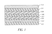
- Figure 1 is a schematic diagram showing a cross-section of a typical organic EL device of the invention containing an interlayer useful in the invention.
- the EL device of the invention is generally as described above. It comprises a compound containing a 3-phenylindolyl group as illustrated in Formula F-1 : wherein R 1 and R 4 represent hydrogen, or an (cyclo)alkyl, or aromatic (carbocyclic or heterocyclic) group and R 2 and R 3 represent hydrogen or one or more optional independently selected substituents on each ring.
- R 1 and R 4 represent hydrogen, or an (cyclo)alkyl, or aromatic (carbocyclic or heterocyclic) group and R 2 and R 3 represent hydrogen or one or more optional independently selected substituents on each ring.
- the compound containing a 3-phenylindolyl group is located in an interlayer (IL) located between a hole-transporting layer and the light emitting layer, and may be in contact with one or both layers.
- the interlayer suitably has a thickness of from 0.1 to 90 nm, typically 0.1 to 25nm and conveniently 0.1 to 15nm.
- the IL will contain a compound represented by Formula F-1 wherein R 2 and R 3 may be independently selected from:
- R 4 is individually selected from Groups 1, 2, 3, and 4; and R 1 is individually selected from Groups 1, 2, 3, 4, and 5.
- the IL contains a compound represented by Formula F-2 : wherein R 4 and R 8 represent a substituent individually selected from Groups 1, 2, 3, and 4; and wherein R 2 , R 3 , R 6 , and R 7 represent one or more substituents on each ring where each substituent is individually selected from the Groups 1 -6 above and Ar is an aromatic group.
- group means any group or atom other than hydrogen.
- substituent group when reference is made in this application to a compound or group that contains a substitutable hydrogen, it is also intended to encompass not only the unsubstituted form, but also its form further substituted with any substituent group or groups as herein mentioned, so long as the substituent does not destroy properties necessary for the intended utility.
- a substituent group may be halogen or may be bonded to the remainder of the molecule by an atom of carbon, silicon, oxygen, nitrogen, phosphorous, or sulfur.
- the substituent may be, for example, halogen, such as chlorine, bromine or fluorine; nitro; hydroxyl; cyano; carboxyl; or groups which may be further substituted, such as alkyl, including straight or branched chain or cyclic alkyl, such as methyl, trifluoromethyl, ethyl, t -butyl, 3-(2,4-di- t -pentylphenoxy) propyl, cyclohexyl, and tetradecyl; alkenyl, such as ethylene, 2-butene; alkoxy, such as methoxy, ethoxy, propoxy, butoxy, 2-methoxyethoxy, sec -butoxy, hexyloxy, 2-ethylhexyloxy, tetradecyloxy, 2-(2,4-di- t -pentylphenoxy)ethoxy, and 2-dodecyloxyethoxy; aryl such as phen
- substituents may themselves be further substituted one or more times with the described substituent groups.
- the particular substituents used may be selected by those skilled in the art to attain the desired desirable properties for a specific application.
- the substituents may be joined together to form a ring such as a fused ring unless otherwise provided.
- the present invention can be employed in most OLED device configurations. These include very simple structures comprising a single anode and cathode to more complex devices, such as passive matrix displays comprised of orthogonal arrays of anodes and cathodes to form pixels, and active-matrix displays where each pixel is controlled independently, for example, with a thin film transistor (TFT).
- TFT thin film transistor
- FIG. 1 A more typical structure is shown in Figure 1 and contains a substrate 101 , an anode 103 , an optional hole-injecting layer 105 , a hole-transporting layer 107 , an interlayer 108 , a light-emitting layer 109 , an electron-transporting layer 111 , and a cathode 113 . These layers are described in detail below. Note that the substrate may alternatively be located adjacent to the cathode, or the substrate may actually constitute the anode or cathode. Also, the total combined thickness of the organic layers is preferably less than 500 nm.
- the substrate 101 can either be light transmissive or opaque, depending on the intended direction of light emission.
- the light transmissive property is desirable for viewing the EL emission through the substrate.
- Transparent glass or organic material are commonly employed in such cases.
- the transmissive characteristic of the bottom support is immaterial, and therefore can be light transmissive, light absorbing or light reflective.
- Substrates for use in this case include, but are not limited to, glass, plastic, semiconductor materials, ceramics, and circuit board materials. Of course it is necessary to provide in these device configurations a light-transparent top electrode.
- the conductive anode layer 103 is commonly formed over the substrate and, when EL emission is viewed through the anode, should be transparent or substantially transparent to the emission of interest.
- Common transparent anode materials used in this invention are indium-tin oxide (ITO) and tin oxide, but other metal oxides can work including, but not limited to, aluminum- or indium-doped zinc oxide (IZO), magnesium-indium oxide, and nickel-tungsten oxide.
- ITO indium-tin oxide
- IZO aluminum- or indium-doped zinc oxide
- IZO aluminum- or indium-doped zinc oxide
- nickel-tungsten oxide nickel-tungsten oxide.
- metal nitrides such as gallium nitride
- metal selenides such as zinc selenide
- metal sulfides such as zinc sulfide
- the transmissive characteristics of layer 103 are immaterial and any conductive material can be used, transparent, opaque or reflective.
- Example conductors for this application include, but are not limited to, gold, iridium, molybdenum, palladium, and platinum.
- Typical anode materials, transmissive or otherwise, have a work function of 4.1 eV or greater. Desired anode materials are commonly deposited by any suitable means such as evaporation, sputtering, chemical vapor deposition, or electrochemical means. Anodes can be patterned using well-known photolithographic processes.
- HIL Hole-Injecting Layer
- a hole-injecting layer 105 be provided between anode 103 and hole-transporting layer 107 .
- the hole-injecting material can serve to improve the film formation property of subsequent organic layers and to facilitate injection of holes into the hole-transporting layer.
- Suitable materials for use in the hole-injecting layer include, but are not limited to, porphyrinic compounds such as those described in US 4,720,432, and plasma-deposited fluorocarbon polymers such as those described in US 6,208,075.
- Alternative hole-injecting materials reportedly useful in organic EL devices are described in EP 0 891 121 A1 and EP 1 029 909 A1.
- HTL Hole-Transporting Layer
- the hole-transporting layer 107 of the organic EL device contains at least one hole-transporting compound such as an aromatic tertiary amine, where the latter is understood to be a compound containing at least one trivalent nitrogen atom that is bonded only to carbon atoms, at least one of which is a member of an aromatic ring.
- the aromatic tertiary amine can be an arylamine, such as a monoarylamine, diarylamine, triarylamine, or a polymeric arylamine group. Exemplary monomeric triarylamines are illustrated by Klupfel et al. US 3,180,730. Other suitable triarylamines substituted with one or more vinyl groups and/or comprising at least one active hydrogen containing group are disclosed by Brantley et al US 3,567,450 and US 3,658,520.
- a more preferred class of aromatic tertiary amines are those which include at least two aromatic tertiary amine moieties as described in US 4,720,432 and US 5,061,569.
- Such compounds include those represented by structural formula (A). wherein Q 1 and Q 2 are independently selected aromatic tertiary amine moieties and G is a linking group such as an arylene, cycloalkylene, or alkylene group of a carbon to carbon bond.
- at least one of Q 1 or Q 2 contains a polycyclic fused ring group, e.g., a naphthalene.
- G is an aryl group, it is conveniently a phenylene, biphenylene, or naphthalene group.
- a useful class of triarylamine groups satisfying structural formula (A) and containing two triarylamine groups is represented by structural formula (B): where R 1 and R 2 each independently represents a hydrogen atom, an aryl group, or an alkyl group or R 1 and R 2 together represent the atoms completing a cycloalkyl group; and R 3 and R 4 each independently represents an aryl group, which is in turn substituted with a diaryl substituted amino group, as indicated by structural formula (C): wherein R 5 and R 6 are independently selected aryl groups.
- at least one of R 5 or R 6 contains a polycyclic fused ring group, e.g., a naphthalene.
- tetraaryldiamines Another class of aromatic tertiary amine groups are the tetraaryldiamines. Desirable tetraaryldiamines groups include two diarylamino groups, such as indicated by formula (C), linked through an arylene group. Useful tetraaryldiamines include those represented by formula (D). wherein each Are is an independently selected arylene group, such as a phenylene or anthracene group, n is an integer of from 1 to 4, and Ar, R 7 , R 8 , and R 9 are independently selected aryl groups. In a typical embodiment, at least one of Ar, R 7 , R 8 , and R 9 is a polycyclic fused ring group, e.g., a naphthalene
- the various alkyl, alkylene, aryl, and arylene groups of the foregoing structural formulae (A), (B), (C), (D), can each in turn be substituted.
- Typical substituents include alkyl groups, alkoxy groups, aryl groups, aryloxy groups, and halogen such as fluoride, chloride, and bromide.
- the various alkyl and alkylene groups typically contain from 1 to 6 carbon atoms.
- the cycloalkyl moieties can contain from 3 to 10 carbon atoms, but typically contain five, six, or seven ring carbon atoms--e.g., cyclopentyl, cyclohexyl, and cycloheptyl ring structures.
- the aryl and arylene groups are usually phenyl and phenylene moieties.
- the hole-transporting layer can be formed of a single or a mixture of aromatic tertiary amine compounds.
- a triarylamine such as a triarylamine satisfying the formula (B)
- a tetraaryldiamine such as indicated by formula (D).
- a triarylamine is employed in combination with a tetraaryldiamine, the latter is positioned as a layer interposed between the triarylamine and the electron injecting and transporting layer.
- useful aromatic tertiary amines are the following:
- Another class of useful hole-transporting materials includes polycyclic aromatic compounds as described in EP 1 009 041.
- polymeric hole-transporting materials can be used such as poly(N-vinylcarbazole) (PVK), polythiophenes, polypyrrole, polyaniline, and copolymers such as poly(3,4-ethylenedioxythiophene) / poly(4-styrenesulfonate) also called PEDOT/PSS.
- the light-emitting layer (LEL) 109 of the organic EL element comprises a luminescent or fluorescent material where electroluminescence is produced as a result of electron-hole pair recombination in this region.
- the light-emitting layer can be comprised of a single material, but more commonly consists of a host material doped with a guest compound or compounds where light emission comes primarily from the dopant and can be of any color.
- the host materials in the light-emitting layer can be an electron-transporting material, as defined below, a hole-transporting material, as defined above, or another material or combination of materials that support hole-electron recombination.
- the dopant is usually chosen from highly fluorescent dyes, but phosphorescent compounds, e.g., transition metal complexes as described in WO 98/55561, WO 00/18851, WO 00/57676, and WO 00/70655 are also useful. Dopants are typically coated as 0.01 to 10 % by weight into the host material.
- Host and emitting molecules known to be of use include, but are not limited to, those disclosed in US 4,768,292, US 5,141,671, US 5,150,006, US 5,151,629, US 5,405,709, US 5,484,922, US 5,593,788, US 5,645,948, US 5,683,823, US 5,755,999, US 5,928,802, US 5,935,720, US 5,935,721, and US 6,020,078.
- Form E Metal complexes of 8-hydroxyquinoline and similar derivatives constitute one class of useful host compounds capable of supporting electroluminescence, and are particularly suitable for light emission of wavelengths longer than 500 nm, e.g., green, yellow, orange, and red.
- M represents a metal
- n is an integer of from 1 to 4
- Z independently in each occurrence represents the atoms completing a nucleus having at least two fused aromatic rings.
- the metal can be monovalent, divalent, trivalent, or tetravalent metal.
- the metal can, for example, be an alkali metal, such as lithium, sodium, or potassium; an alkaline earth metal, such as magnesium or calcium; an earth metal, such aluminum or gallium, or a transition metal such as zinc or zirconium.
- alkali metal such as lithium, sodium, or potassium
- alkaline earth metal such as magnesium or calcium
- earth metal such aluminum or gallium, or a transition metal such as zinc or zirconium.
- any monovalent, divalent, trivalent, or tetravalent metal known to be a useful chelating metal can be employed.
- Z completes a heterocyclic nucleus containing at least two fused aromatic rings, at least one of which is an azole or azine ring. Additional rings, including both aliphatic and aromatic rings, can be fused with the two required rings, if required. To avoid adding molecular bulk without improving on function the number of ring atoms is usually maintained at 18 or less.
- Illustrative of useful chelated oxinoid compounds are the following:
- Formula F Derivatives of 9,10-di-(2-naphthyl)anthracene (Formula F) constitute one class of useful hosts capable of supporting electroluminescence, and are particularly suitable for light emission of wavelengths longer than 400 nm, e.g., blue, green, yellow, orange or red.
- R 1 , R 2 , R 3 , R 4 , R 5 , and R 6 represent hydrogen or one or more substituents selected from the following groups:
- Illustrative examples include 9,10-di-(2-naphthyl)anthracene and 2- t -butyl-9,10-di-(2-naphthyl)anthracene.
- Other anthracene derivatives can be useful as a host in the LEL, including derivatives of 9,10-bis[4-(2,2-diphenylethenyl)phenyl]anthracene.
- Benzazole derivatives constitute another class of useful hosts capable of supporting electroluminescence, and are particularly suitable for light emission of wavelengths longer than 400 nm, e.g., blue, green, yellow, orange or red.
- n is an integer of 3 to 8
- Z is -O, -NR or -S where R is H or a substituent
- R' represents one or more optional substituents where R and each R' are H or alkyl groups such as propyl, t-butyl, and heptyl groups typically having from 1 to 24 carbon atoms; carbocyclic or heterocyclic ring groups such as phenyl and naphthyl, furyl, thienyl, pyridyl, and quinolinyl groups and atoms necessary to complete a fused aromatic ring group typically having from 5 to 20 carbon atoms; and halo such as chloro, and fluoro;
- L is a linkage unit usually comprising an alkyl or aryl group
- An example of a useful benzazole is 2, 2', 2"-(1,3,5-phenylene)tris[1-phenyl-1H-benzimidazole].
- Desirable fluorescent dopants include groups derived from fused ring, heterocyclic and other compounds such as anthracene, tetracene, xanthene, perylene, rubrene, coumarin, rhodamine, quinacridone, dicyanomethylenepyran, thiopyran , polymethine, pyrilium thiapyrilium, and carbostyryl compounds.
- useful dopants include, but are not limited to, the following:
- ETL Electron-Transporting Layer
- Preferred thin film-forming materials for use in forming the electron-transporting layer 111 of the organic EL devices of this invention are metal chelated oxinoid compounds, including chelates of oxine itself (also commonly referred to as 8-quinolinol or 8-hydroxyquinoline). Such compounds help to inject and transport electrons and exhibit both high levels of performance and are readily fabricated in the form of thin films.
- exemplary of contemplated oxinoid compounds are those satisfying structural formula (E), previously described.
- electron-transporting materials include various butadiene derivatives as disclosed in US 4,356,429 and various heterocyclic optical brighteners as described in US 4,539,507. Benzazoles satisfying structural formula (G) are also useful electron transporting materials.
- layers 109 and 111 can optionally be collapsed into a single layer that serves the function of supporting both light emission and electron transportation.
- the cathode layer 113 used in this invention can be comprised of nearly any conductive material. Desirable materials have good film-forming properties to ensure good contact with the underlying organic layer, promote electron injection at low voltage, and have good stability. Useful cathode materials often contain a low work function metal ( ⁇ 4.0 eV) or metal alloy. One preferred cathode material is comprised of a Mg:Ag alloy wherein the percentage of silver is in the range of 1 to 20 %, as described in US 4,885,221. Another suitable class of cathode materials includes bilayers comprised of a thin layer of a low work function metal or metal salt capped with a thicker layer of conductive metal.
- cathode is comprised of a thin layer of LiF followed by a thicker layer of A1 as described in US 5,677,572.
- Other useful cathode materials include, but are not limited to, those disclosed in US 5,059,861, US 5,059,862, and US 6,140,763.
- cathode When light emission is viewed through the cathode, the cathode must be transparent or nearly transparent. For such applications, metals must be thin or one must use transparent conductive oxides, or a combination of these materials.
- Optically transparent cathodes have been described in more detail in US 5,776,623. Cathode materials can be deposited by evaporation, sputtering, or chemical vapor deposition. When needed, patterning can be achieved through many well known methods including, but not limited to, through-mask deposition, integral shadow masking as described in US 5,276,380 and EP 0 732 868, laser ablation, and selective chemical vapor deposition.
- the organic materials mentioned above are suitably deposited through sublimation, but can be deposited from a solvent with an optional binder to improve film formation. If the material is a polymer, solvent deposition is usually preferred.
- the material to be deposited by sublimation can be vaporized from a sublimator "boat" often comprised of a tantalum material, e.g., as described in US 6,237,529, or can be first coated onto a donor sheet and then sublimed in closer proximity to the substrate. Layers with a mixture of materials can utilize separate sublimator boats or the materials can be pre-mixed and coated from a single boat or donor sheet.
- Patterned deposition can be achieved using shadow masks, integral shadow masks (US 5,294,870), spatially-defined thermal dye transfer from a donor sheet (US 5,851,709 and US 6,066,357) and inkjet method (US 6,066,357).
- OLED devices are sensitive to moisture and/or oxygen so they are commonly sealed in an inert atmosphere such as nitrogen or argon, along with a desiccant such as alumina, bauxite, calcium sulfate, clays, silica gel, zeolites, alkaline metal oxides, alkaline earth metal oxides, sulfates, or metal halides and perchlorates.
- a desiccant such as alumina, bauxite, calcium sulfate, clays, silica gel, zeolites, alkaline metal oxides, alkaline earth metal oxides, sulfates, or metal halides and perchlorates.
- Titanium trichloride (0.43g, 2.81mmol), zinc (9.2g, 14mmol), and trimethylsilyl chloride (17.8mL, 14mmol) was added to a mixture of amide S-1 (7.0g, 9.36mmol) in 1,2-dimethoxyethane (93mL). The mixture was heated to 110°C for 8 hours, then cooled to room temperature. The mixture was filtered through a pad of silica gel with methylene chloride. The filtrate was concentrated with a rotary evaporator and recrystallized from ethyl acetate and heptane to yield S-2.
- a series of EL devices satisfying the requirements of the invention were constructed in the following manner: A glass substrate coated with an 42 nm layer of indium-tin oxide (ITO) as the anode was sequentially ultrasonicated in a commercial detergent, rinsed in deionized water, degreased in toluene vapor and exposed to oxygen plasma for about 1 min.
- ITO indium-tin oxide
- a comparison device was prepared omitting layer c) and containing an overall device layer thickness substantially the same as the other examples.
- the inventive samples provide an improved luminance over the corresponding comparison samples.
- Sample 3-1 represents a HTL of NPB only and Sample 3-7 represents a HTL containing I-1 only. It is noted that the use of I-1 in the HTL improves the luminance vs. NPB, but at an extreme penalty for voltage requires.
- the inventive devices exhibit improved relative luminance with little or no increase in voltage requirement.
- Embodiments of the invention include the device where where: the IL is between 0.1 and 90nm or desirably between 0.1 and 15nm thick; the HTL contains an aromatic tertiary amine group containing at least one trivalent nitrogen atom that is bonded only to carbon atoms, at least one of which is a member of an aromatic ring group; the LEL contains a dopant in an amount of 0.01 to 20% by weight; the ETL contains tris(8-quinolinolato)aluminum(III); the LEL contains a compound having formula I: wherein M represents a metal; n is an integer of from 1 to 3; and Z independently in each occurrence represents the atoms completing a nucleus having at least two fused aromatic rings; the LEL contains a compound that fluoresces with the color red; R 1 in formula F-1 is an aromatic group of from 5 to 20 carbon atoms such as one represented by Formula II: wherein R 5 represents one or more substituents on the aromatic ring where each is independently selected
- R 4 and R 8 are independently selected from Groups 1, 2, 3, and 4 as above,
- Ar is a para-substituted phenyl group such as a 4,4'-substituted biphenyl group or a 1,3,5-trisubstituted phenyl group, wherein each of the substituents is a 3-phenylindolyl group; the compound containing a 3-phenylindolyl group contains at least two 3-phenylindolyl groups; and includes a static or motion imaging device incorporating the device of the invention.
Landscapes
- Chemical & Material Sciences (AREA)
- Engineering & Computer Science (AREA)
- Materials Engineering (AREA)
- Organic Chemistry (AREA)
- Physics & Mathematics (AREA)
- Spectroscopy & Molecular Physics (AREA)
- Electroluminescent Light Sources (AREA)
Abstract
Description
- This invention relates to organic electroluminescent devices that emit light from a current- conducting organic light emitting layer and have high luminance where the device employs a particular interlayer between a hole transport layer and the light emitting layer.
- While organic electroluminescent (EL) devices have been known for over two decades, their performance limitations have represented a barrier to many desirable applications. In simplest form, an organic EL device is comprised of an anode for hole injection, a cathode for electron injection, and an organic medium electroluminescent element sandwiched between these electrodes to support charge recombination that yields emission of light. These devices are also commonly referred to as organic light-emitting diodes, or OLEDs. Representative of earlier organic EL devices are Gurnee et al. U.S. Pat. No. 3,172,862, issued Mar. 9, 1965; Gurnee U.S. Pat. No. 3,173,050, issued Mar. 9, 1965; Dresner, "Double Injection Electroluminescence in Anthracene", RCA Review, Vol. 30, pp. 322-334, 1969; and Dresner U.S. Pat. No. 3,710,167, issued Jan. 9, 1973. The organic layers in these devices, usually composed of a polycyclic aromatic hydrocarbons, were very thick (much greater than 1 µm). Consequently, operating voltages were very high, often >100V.
- More recent organic EL devices include an organic EL element consisting of extremely thin layers (e.g. <1.0 µm) between the anode and the cathode. Herein, the organic "EL element" encompasses the layers between the anode and cathode electrodes. Reducing the thickness lowered the resistance of the organic layer and has enabled devices that operate much lower voltage. In a basic EL element structure, described in US 4,356,429, one organic layer of the EL element adjacent to the anode is specifically chosen to transport holes, therefore, it is referred to as the hole transporting layer (HTL), and the other organic layer is specifically chosen to transport electrons, referred to as the electron transporting layer (ETL). The interface between the two layers provides an efficient site for the recombination of the injected hole/electron pair and the resultant electroluminescence.
- There have been proposed organic EL elements that contain an organic light-emitting layer (LEL) between a hole- transporting layer and an electron-transporting layer, such as that disclosed by Tang et al [J. Applied Physics, Vol. 65, Pages 3610-3616, 1989]. The light-emitting layer commonly consists of a host material doped with a guest material. Still further, there has been proposed in US 4,769,292 a four-layer EL element comprising a hole-injecting layer (HIL), a hole-transporting layer, a light-emitting layer and an electron transport/injection layer. These structures have resulted in improved device efficiency.
- Materials comprising porphyrinic compounds have been disclosed by Tang in US 4,356,429 for use in the HTL. Further improvements in device performance are taught in US 4,539,507, US 4,720,432, and US 5,061,569 where the hole-transporting layer utilizes an aromatic tertiary amine.
- Since these early inventions, further improvements in hole-transporting and other device materials have resulted in improved device performance in attributes such as color, stability, luminance efficiency and manufacturability, e.g., as disclosed in US 5,061,569, US 5,409,783, US 5,554,450, US 5,593,788, US 5,683,823, US 5, 908,581, US 5,928,802, US 6,020,078, and US 6,208,077, amongst others. EP 891,121 and EP 1.029,909 suggest the use of biphenylene and phenylene diamine derivatives to improve hole injecting and/or transporting and JP 11-273830 suggests the use of naphthyldiamine derivatives in EL elements generally.
- In JP 2001-118,683 and in JP 05-339,565 OLED devices have been suggested that include 3-phenylindolyl groups in the HTL or the LEL. Such materials have not been suggested in an interlayer between the HTL and the LEL.
- Notwithstanding the foregoing developments, there are continuing needs for organic EL device components that, at a given current, will provide a desired high luminance with little or no increase in voltage necessary to obtain the luminance.
- The invention provides a multilayer electroluminescent device comprising an anode, a hole transport layer (HTL), a light emitting layer (LEL), an electron transport layer (ETL), and a cathode, in that order, wherein there is located between the HTL and the LEL an interlayer (IL) comprising a compound containing a 3-phenylindolyl group. The invention also provides an imaging device containing such an electroluminescent device.
- The device of the invention produces improved luminance with little or no increase in voltage necessary to obtain the luminance.
- Figure 1 is a schematic diagram showing a cross-section of a typical organic EL device of the invention containing an interlayer useful in the invention.
- The EL device of the invention is generally as described above. It comprises a compound containing a 3-phenylindolyl group as illustrated in Formula F-1:wherein R1 and R4 represent hydrogen, or an (cyclo)alkyl, or aromatic (carbocyclic or heterocyclic) group and R2 and R3 represent hydrogen or one or more optional independently selected substituents on each ring. Within the EL device the compound containing a 3-phenylindolyl group is located in an interlayer (IL) located between a hole-transporting layer and the light emitting layer, and may be in contact with one or both layers. The interlayer suitably has a thickness of from 0.1 to 90 nm, typically 0.1 to 25nm and conveniently 0.1 to 15nm.

- Desirably, the IL will contain a compound represented by Formula F-1 wherein R2 and R3 may be independently selected from:
- Group 1: hydrogen, an alkyl and an alkoxy group, typically of from 1 to 24 carbon atoms;
- Group 2: a ring group, typically of from 5 to 20 carbon atoms;
- Group 3: the atoms necessary to complete a carbocyclic fused group, typically of from 4 to 24 carbon atoms, such as an anthracenyl, pyrenyl, and perylenyl group;
- Group 4: the atoms necessary to complete a heterocyclic fused ring group, typically of from 5 to 24 carbon atoms, as necessary to complete a fused hetero ring such as a furyl, thienyl, pyridyl, or quinolinyl group;
- Group 5: an aryloxy, alkylamino, and arylamino group, typically of from 1 to 24 carbon atoms; and
- Group 6: fluorine, chlorine, bromine and cyano groups.
-
- R4 is individually selected from Groups 1, 2, 3, and 4; and R1 is individually selected from Groups 1, 2, 3, 4, and 5.
- More typically the IL contains a compound represented by Formula F-2:wherein R4 and R8 represent a substituent individually selected from Groups 1, 2, 3, and 4; and wherein R2, R3, R6, and R7 represent one or more substituents on each ring where each substituent is individually selected from the Groups 1 -6 above and Ar is an aromatic group.

- Illustrative examples of compounds containing a 3-phenylindolyl group useful in the present invention are the following:


- Unless otherwise specifically stated, use of the term "group", "substituted" or "substituent" means any group or atom other than hydrogen. Additionally, when reference is made in this application to a compound or group that contains a substitutable hydrogen, it is also intended to encompass not only the unsubstituted form, but also its form further substituted with any substituent group or groups as herein mentioned, so long as the substituent does not destroy properties necessary for the intended utility. Suitably, a substituent group may be halogen or may be bonded to the remainder of the molecule by an atom of carbon, silicon, oxygen, nitrogen, phosphorous, or sulfur. The substituent may be, for example, halogen, such as chlorine, bromine or fluorine; nitro; hydroxyl; cyano; carboxyl; or groups which may be further substituted, such as alkyl, including straight or branched chain or cyclic alkyl, such as methyl, trifluoromethyl, ethyl, t-butyl, 3-(2,4-di-t-pentylphenoxy) propyl, cyclohexyl, and tetradecyl; alkenyl, such as ethylene, 2-butene; alkoxy, such as methoxy, ethoxy, propoxy, butoxy, 2-methoxyethoxy, sec-butoxy, hexyloxy, 2-ethylhexyloxy, tetradecyloxy, 2-(2,4-di-t-pentylphenoxy)ethoxy, and 2-dodecyloxyethoxy; aryl such as phenyl, 4-t-butylphenyl, 2,4,6-trimethylphenyl, naphthyl; aryloxy, such as phenoxy, 2-methylphenoxy, alpha- or beta-naphthyloxy, and 4-tolyloxy; carbonamido, such as acetamido, benzamido, butyramido, tetradecanamido, alpha-(2,4-di-t-pentyl-phenoxy)acetamido, alpha-(2,4-di-t-pentylphenoxy)butyramido, alpha-(3-pentadecylphenoxy)-hexanamido, alpha-(4-hydroxy-3-t-butylphenoxy)-tetradecanamido, 2-oxo-pyrrolidin-1-yl, 2-oxo-5-tetradecylpyrrolin-1-yl, N-methyltetradecanamido, N-succinimido, N-phthalimido, 2,5-dioxo-1-oxazolidinyl, 3-dodecyl-2,5-dioxo-1-imidazolyl,and N-acetyl-N-dodecylamino, ethoxycarbonylamino, phenoxycarbonylamino, benzyloxycarbonylamino, hexadecyloxycarbonylamino, 2,4-di-t-butylphenoxycarbonylamino, phenylcarbonylamino, 2,5-(di-t-pentylphenyl)carbonylamino, p-dodecyl-phenylcarbonylamino, p-tolylcarbonylamino, N-methylureido, N,N-dimethylureido, N-methyl-N-dodecylureido, N-hexadecylureido, N,N-dioctadecylureido, N,N-dioctyl-N'-ethylureido, N-phenylureido, N,N-diphenylureido, N-phenyl-N-p-tolylureido, N-(m-hexadecylphenyl)ureido, N,N-(2,5-di-t-pentylphenyl)-N'-ethylureido, and t-butylcarbonamido; sulfonamido, such as methylsulfonamido, benzenesulfonamido, p-tolylsulfonamido, p-dodecylbenzenesulfonamido, N-methyltetradecylsulfonamido, N,N-dipropyl-sulfamoylamino, and hexadecylsulfonamido; sulfamoyl, such as N-methylsulfamoyl, N-ethylsulfamoyl, N,N-dipropylsulfamoyl, N-hexadecylsulfamoyl, N,N-dimethylsulfamoyl; N-[3-(dodecyloxy)propyl]sulfamoyl, N-[4-(2,4-di-t-pentylphenoxy)butyl]sulfamoyl, N-methyl-N-tetradecylsulfamoyl, and N-dodecylsulfamoyl; carbamoyl, such as N-methylcarbamoyl, N,N-dibutylcarbamoyl, N-octadecylcarbamoyl, N-[4-(2,4-di-t-pentylphenoxy)butyl]carbamoyl, N-methyl-N-tetradecylcarbamoyl, and N,N-dioctylcarbamoyl; acyl, such as acetyl, (2,4-di-t-amylphenoxy)acetyl, phenoxycarbonyl, p-dodecyloxyphenoxycarbonyl methoxycarbonyl, butoxycarbonyl, tetradecyloxycarbonyl, ethoxycarbonyl, benzyloxycarbonyl, 3-pentadecyloxycarbonyl, and dodecyloxycarbonyl; sulfonyl, such as methoxysulfonyl, octyloxysulfonyl, tetradecyloxysulfonyl, 2-ethylhexyloxysulfonyl, phenoxysulfonyl, 2,4-di-t-pentylphenoxysulfonyl, methylsulfonyl, octylsulfonyl, 2-ethylhexylsulfonyl, dodecylsulfonyl, hexadecylsulfonyl, phenylsulfonyl, 4-nonylphenylsulfonyl, and p-tolylsulfonyl; sulfonyloxy, such as dodecylsulfonyloxy, and hexadecylsulfonyloxy; sulfinyl, such as methylsulfinyl, octylsulfinyl, 2-ethylhexylsulfinyl, dodecylsulfinyl, hexadecylsulfinyl, phenylsulfinyl, 4-nonylphenylsulfinyl, and p-tolylsulfinyl; thio, such as ethylthio, octylthio, benzylthio, tetradecylthio, 2-(2,4-di-t-pentylphenoxy)ethylthio, phenylthio, 2-butoxy-5-t-octylphenylthio, and p-tolylthio; acyloxy, such as acetyloxy, benzoyloxy, octadecanoyloxy, p-dodecylamidobenzoyloxy, N-phenylcarbamoyloxy, N-ethylcarbamoyloxy, and cyclohexylcarbonyloxy; amine, such as phenylanilino, 2-chloroanilino, diethylamine, dodecylamine; imino, such as 1 (N-phenylimido)ethyl, N-succinimido or 3-benzylhydantoinyl; phosphate, such as dimethylphosphate and ethylbutylphosphate; phosphite, such as diethyl and dihexylphosphite; a heterocyclic group, a heterocyclic oxy group or a heterocyclic thio group, each of which may be substituted and which contain a 3 to 7 membered heterocyclic ring composed of carbon atoms and at least one hetero atom selected from the group consisting of oxygen, nitrogen and sulfur, such as 2-furyl, 2-thienyl, 2-benzimidazolyloxy or 2-benzothiazolyl; quaternary ammonium, such as triethylammonium; and silyloxy, such as trimethylsilyloxy.
- If desired, the substituents may themselves be further substituted one or more times with the described substituent groups. The particular substituents used may be selected by those skilled in the art to attain the desired desirable properties for a specific application. When a molecule may have two or more substituents, the substituents may be joined together to form a ring such as a fused ring unless otherwise provided.
- The present invention can be employed in most OLED device configurations. These include very simple structures comprising a single anode and cathode to more complex devices, such as passive matrix displays comprised of orthogonal arrays of anodes and cathodes to form pixels, and active-matrix displays where each pixel is controlled independently, for example, with a thin film transistor (TFT).
- There are numerous configurations of the organic layers wherein the present invention can be successfully practiced. Essential requirements are a cathode, an anode, an HTL and an LEL. A more typical structure is shown in Figure 1 and contains a
substrate 101, ananode 103, an optional hole-injectinglayer 105, a hole-transporting layer 107, aninterlayer 108, a light-emitting layer 109, an electron-transporting layer 111, and acathode 113. These layers are described in detail below. Note that the substrate may alternatively be located adjacent to the cathode, or the substrate may actually constitute the anode or cathode. Also, the total combined thickness of the organic layers is preferably less than 500 nm. - The
substrate 101 can either be light transmissive or opaque, depending on the intended direction of light emission. The light transmissive property is desirable for viewing the EL emission through the substrate. Transparent glass or organic material are commonly employed in such cases. For applications where the EL emission is viewed through the top electrode, the transmissive characteristic of the bottom support is immaterial, and therefore can be light transmissive, light absorbing or light reflective. Substrates for use in this case include, but are not limited to, glass, plastic, semiconductor materials, ceramics, and circuit board materials. Of course it is necessary to provide in these device configurations a light-transparent top electrode. - The
conductive anode layer 103 is commonly formed over the substrate and, when EL emission is viewed through the anode, should be transparent or substantially transparent to the emission of interest. Common transparent anode materials used in this invention are indium-tin oxide (ITO) and tin oxide, but other metal oxides can work including, but not limited to, aluminum- or indium-doped zinc oxide (IZO), magnesium-indium oxide, and nickel-tungsten oxide. In addition to these oxides, metal nitrides, such as gallium nitride, and metal selenides, such as zinc selenide, and metal sulfides, such as zinc sulfide, can be used inlayer 103. For applications where EL emission is viewed through the top electrode, the transmissive characteristics oflayer 103 are immaterial and any conductive material can be used, transparent, opaque or reflective. Example conductors for this application include, but are not limited to, gold, iridium, molybdenum, palladium, and platinum. Typical anode materials, transmissive or otherwise, have a work function of 4.1 eV or greater. Desired anode materials are commonly deposited by any suitable means such as evaporation, sputtering, chemical vapor deposition, or electrochemical means. Anodes can be patterned using well-known photolithographic processes. - While not always necessary, it is often useful that a hole-injecting
layer 105 be provided betweenanode 103 and hole-transportinglayer 107. The hole-injecting material can serve to improve the film formation property of subsequent organic layers and to facilitate injection of holes into the hole-transporting layer. Suitable materials for use in the hole-injecting layer include, but are not limited to, porphyrinic compounds such as those described in US 4,720,432, and plasma-deposited fluorocarbon polymers such as those described in US 6,208,075. Alternative hole-injecting materials reportedly useful in organic EL devices are described in EP 0 891 121 A1 and EP 1 029 909 A1. - The hole-transporting
layer 107 of the organic EL device contains at least one hole-transporting compound such as an aromatic tertiary amine, where the latter is understood to be a compound containing at least one trivalent nitrogen atom that is bonded only to carbon atoms, at least one of which is a member of an aromatic ring. In one form the aromatic tertiary amine can be an arylamine, such as a monoarylamine, diarylamine, triarylamine, or a polymeric arylamine group. Exemplary monomeric triarylamines are illustrated by Klupfel et al. US 3,180,730. Other suitable triarylamines substituted with one or more vinyl groups and/or comprising at least one active hydrogen containing group are disclosed by Brantley et al US 3,567,450 and US 3,658,520. - A more preferred class of aromatic tertiary amines are those which include at least two aromatic tertiary amine moieties as described in US 4,720,432 and US 5,061,569. Such compounds include those represented by structural formula (A).wherein Q1 and Q2 are independently selected aromatic tertiary amine moieties and G is a linking group such as an arylene, cycloalkylene, or alkylene group of a carbon to carbon bond. In one embodiment, at least one of Q1 or Q2 contains a polycyclic fused ring group, e.g., a naphthalene. When G is an aryl group, it is conveniently a phenylene, biphenylene, or naphthalene group.

- A useful class of triarylamine groups satisfying structural formula (A) and containing two triarylamine groups is represented by structural formula (B):where

R1 and R2 each independently represents a hydrogen atom, an aryl group, or an alkyl group or R1 and R2 together represent the atoms completing a cycloalkyl group; and
R3 and R4 each independently represents an aryl group, which is in turn substituted with a diaryl substituted amino group, as indicated by structural formula (C):wherein R5 and R6 are independently selected aryl groups. In one embodiment, at least one of R5 or R6 contains a polycyclic fused ring group, e.g., a naphthalene.
- Another class of aromatic tertiary amine groups are the tetraaryldiamines. Desirable tetraaryldiamines groups include two diarylamino groups, such as indicated by formula (C), linked through an arylene group. Useful tetraaryldiamines include those represented by formula (D).wherein

each Are is an independently selected arylene group, such as a phenylene or anthracene group,
n is an integer of from 1 to 4, and
Ar, R7, R8, and R9 are independently selected aryl groups. In a typical embodiment, at least one of Ar, R7, R8, and R9 is a polycyclic fused ring group, e.g., a naphthalene - The various alkyl, alkylene, aryl, and arylene groups of the foregoing structural formulae (A), (B), (C), (D), can each in turn be substituted. Typical substituents include alkyl groups, alkoxy groups, aryl groups, aryloxy groups, and halogen such as fluoride, chloride, and bromide. The various alkyl and alkylene groups typically contain from 1 to 6 carbon atoms. The cycloalkyl moieties can contain from 3 to 10 carbon atoms, but typically contain five, six, or seven ring carbon atoms--e.g., cyclopentyl, cyclohexyl, and cycloheptyl ring structures. The aryl and arylene groups are usually phenyl and phenylene moieties.
- The hole-transporting layer can be formed of a single or a mixture of aromatic tertiary amine compounds. Specifically, one may employ a triarylamine, such as a triarylamine satisfying the formula (B), in combination with a tetraaryldiamine, such as indicated by formula (D). When a triarylamine is employed in combination with a tetraaryldiamine, the latter is positioned as a layer interposed between the triarylamine and the electron injecting and transporting layer. Illustrative of useful aromatic tertiary amines are the following:
- 1,1 -Bis(4-di- p -tolylaminophenyl)cyclohexane
- 1,1 -Bis(4-di- p -tolylaminophenyl)-4-phenylcyclohexane
- 4,4'-Bis(diphenylamino)quadriphenyl
- Bis(4-dimethylamino-2-methylphenyl)-phenylmethane
- N,N,N-Tri( p -tolyl)amine
- 4-(di-p-tolylamino)-4'-[4(di- p -tolylamino)-styryl]stilbene N,N,N',N'-Tetra- p -tolyl-4-4'-diaminobiphenyl
- N,N,N',N'-Tetraphenyl-4,4'-diaminobiphenyl
- N,N,N',N'-tetra-1-naphthyl-4,4'-diaminobiphenyl
- N,N,N',N'-tetra-2-naphthyl-4,4'-diaminobiphenyl
- N-Phenylcarbazole
- 4,4'-Bis[N-(1-naphthyl)-N-phenylamino]biphenyl
- 4,4'-Bis[N-(1-naphthyl)-N-(2-naphthyl)amino]biphenyl
- 4,4"-Bis[N-(1-naphthyl)-N-phenylamino]p-terphenyl
- 4,4'-Bis[N-(2-naphthyl)-N-phenylamino]biphenyl
- 4,4'-Bis[N-(3-acenaphthenyl)-N-phenylamino]biphenyl
- 1,5-Bis[N-(1-naphthyl)-N-phenylamino]naphthalene
- 4,4'-Bis[N-(9-anthryl)-N-phenylamino]biphenyl
- 4,4"-Bis[N-(1-anthryl)-N-phenylamino]- p -terphenyl
- 4,4'-Bis[N-(2-phenanthryl)-N-phenylamino]biphenyl
- 4,4'-Bis[N-(8-fluoranthenyl)-N-phenylamino]biphenyl
- 4,4'-Bis[N-(2-pyrenyl)-N-phenylamino]biphenyl
- 4,4'-Bis[N-(2-naphthacenyl)-N-phenylamino]biphenyl
- 4,4'-Bis[N-(2-perylenyl)-N-phenylamino]biphenyl
- 4,4'-Bis[N-(1-coronenyl)-N-phenylamino]biphenyl
- 2,6-Bis(di- p -tolylamino)naphthalene
- 2,6-Bis[di-(1-naphthyl)amino]naphthalene
- 2,6-Bis[N-(1-naphthyl)-N-(2-naphthyl)amino]naphthalene
- N,N,N',N'-Tetra(2-naphthyl)-4,4"-diamino-p-terphenyl
- 4,4'-Bis {N-phenyl-N-[4-(1-naphthyl)-phenyl]amino}biphenyl
- 4,4'-Bis[N-phenyl-N-(2-pyrenyl)amino]biphenyl
- 2,6-Bis[N,N-di(2-naphthyl)amine]fluorine
- 1,5-Bis[N-(1-naphthyl)-N-phenylamino]naphthalene
-
- Another class of useful hole-transporting materials includes polycyclic aromatic compounds as described in EP 1 009 041. In addition, polymeric hole-transporting materials can be used such as poly(N-vinylcarbazole) (PVK), polythiophenes, polypyrrole, polyaniline, and copolymers such as poly(3,4-ethylenedioxythiophene) / poly(4-styrenesulfonate) also called PEDOT/PSS.
- As more fully described in US 4,769,292 and 5,935,721, the light-emitting layer (LEL) 109 of the organic EL element comprises a luminescent or fluorescent material where electroluminescence is produced as a result of electron-hole pair recombination in this region. The light-emitting layer can be comprised of a single material, but more commonly consists of a host material doped with a guest compound or compounds where light emission comes primarily from the dopant and can be of any color. The host materials in the light-emitting layer can be an electron-transporting material, as defined below, a hole-transporting material, as defined above, or another material or combination of materials that support hole-electron recombination. The dopant is usually chosen from highly fluorescent dyes, but phosphorescent compounds, e.g., transition metal complexes as described in WO 98/55561, WO 00/18851, WO 00/57676, and WO 00/70655 are also useful. Dopants are typically coated as 0.01 to 10 % by weight into the host material.
- An important relationship for choosing a dye as a dopant is a comparison of the bandgap potential which is defined as the energy difference between the highest occupied molecular orbital and the lowest unoccupied molecular orbital of the molecule. For efficient energy transfer from the host to the dopant molecule, a necessary condition is that the band gap of the dopant is smaller than that of the host material.
- Host and emitting molecules known to be of use include, but are not limited to, those disclosed in US 4,768,292, US 5,141,671, US 5,150,006, US 5,151,629, US 5,405,709, US 5,484,922, US 5,593,788, US 5,645,948, US 5,683,823, US 5,755,999, US 5,928,802, US 5,935,720, US 5,935,721, and US 6,020,078.
- Metal complexes of 8-hydroxyquinoline and similar derivatives (Formula E) constitute one class of useful host compounds capable of supporting electroluminescence, and are particularly suitable for light emission of wavelengths longer than 500 nm, e.g., green, yellow, orange, and red.wherein

M represents a metal;
n is an integer of from 1 to 4; and
Z independently in each occurrence represents the atoms completing a nucleus having at least two fused aromatic rings. - From the foregoing it is apparent that the metal can be monovalent, divalent, trivalent, or tetravalent metal. The metal can, for example, be an alkali metal, such as lithium, sodium, or potassium; an alkaline earth metal, such as magnesium or calcium; an earth metal, such aluminum or gallium, or a transition metal such as zinc or zirconium. Generally any monovalent, divalent, trivalent, or tetravalent metal known to be a useful chelating metal can be employed.
- Z completes a heterocyclic nucleus containing at least two fused aromatic rings, at least one of which is an azole or azine ring. Additional rings, including both aliphatic and aromatic rings, can be fused with the two required rings, if required. To avoid adding molecular bulk without improving on function the number of ring atoms is usually maintained at 18 or less.
- Illustrative of useful chelated oxinoid compounds are the following:
- CO-1: Aluminum trisoxine [alias, tris(8-quinolinolato)aluminum(III)]
- CO-2: Magnesium bisoxine [alias, bis(8-quinolinolato)magnesium(II)]
- CO-3: Bis[benzo {f}-8-quinolinolato]zinc (II)
- CO-4: Bis(2-methyl-8-quinolinolato)aluminum(III)-µ-oxo-bis(2-methyl-8-quinolinolato) aluminum(III)
- CO-5: Indium trisoxine [alias, tris(8-quinolinolato)indium]
- CO-6: Aluminum tris(5-methyloxine) [alias, tris(5-methyl-8-quinolinolato) aluminum(III)]
- CO-7: Lithium oxine [alias, (8-quinolinolato)lithium(I)]
- CO-8: Gallium oxine [alias, tris(8-quinolinolato)gallium(III)]
- CO-9: Zirconium oxine [alias, tetra(8-quinolinolato)zirconium(IV)]
-
- Derivatives of 9,10-di-(2-naphthyl)anthracene (Formula F) constitute one class of useful hosts capable of supporting electroluminescence, and are particularly suitable for light emission of wavelengths longer than 400 nm, e.g., blue, green, yellow, orange or red.wherein: R1, R2, R3, R4, R5, and R6 represent hydrogen or one or more substituents selected from the following groups:

- Group 1: hydrogen, alkyl and alkoxy groups typically having from 1 to 24 carbon atoms;
- Group 2: a ring group, typically having from 6 to 20 carbon atoms;
- Group 3: the atoms necessary to complete a carbocyclic fused ring group such as naphthyl, anthracenyl, pyrenyl, and perylenyl groups, typically having from 6 to 30 carbon atoms;
- Group 4: the atoms necessary to complete a heterocyclic fused ring group such as furyl, thienyl, pyridyl, and quinolinyl groups, typically having from 5 to 24 carbon atoms;
- Group 5: an aryloxy, alkylamino, and arylamino group typically having from 1 to 24 carbon atoms; and
- Group 6: fluorine, chlorine, bromine and cyano groups.
-
- Illustrative examples include 9,10-di-(2-naphthyl)anthracene and 2-t-butyl-9,10-di-(2-naphthyl)anthracene. Other anthracene derivatives can be useful as a host in the LEL, including derivatives of 9,10-bis[4-(2,2-diphenylethenyl)phenyl]anthracene.
- Benzazole derivatives (Formula G) constitute another class of useful hosts capable of supporting electroluminescence, and are particularly suitable for light emission of wavelengths longer than 400 nm, e.g., blue, green, yellow, orange or red.where:

n is an integer of 3 to 8;
Z is -O, -NR or -S where R is H or a substituent; and
R' represents one or more optional substituents where R and each R' are H or alkyl groups such as propyl, t-butyl, and heptyl groups typically having from 1 to 24 carbon atoms; carbocyclic or heterocyclic ring groups such as phenyl and naphthyl, furyl, thienyl, pyridyl, and quinolinyl groups and atoms necessary to complete a fused aromatic ring group typically having from 5 to 20 carbon atoms; and halo such as chloro, and fluoro;
L is a linkage unit usually comprising an alkyl or aryl group which conjugately or unconjugately connects the multiple benzazoles together. - An example of a useful benzazole is 2, 2', 2"-(1,3,5-phenylene)tris[1-phenyl-1H-benzimidazole].
- Desirable fluorescent dopants include groups derived from fused ring, heterocyclic and other compounds such as anthracene, tetracene, xanthene, perylene, rubrene, coumarin, rhodamine, quinacridone, dicyanomethylenepyran, thiopyran , polymethine, pyrilium thiapyrilium, and carbostyryl compounds.
- Illustrative examples of useful dopants include, but are not limited to, the following:


- Preferred thin film-forming materials for use in forming the electron-transporting
layer 111 of the organic EL devices of this invention are metal chelated oxinoid compounds, including chelates of oxine itself (also commonly referred to as 8-quinolinol or 8-hydroxyquinoline). Such compounds help to inject and transport electrons and exhibit both high levels of performance and are readily fabricated in the form of thin films. Exemplary of contemplated oxinoid compounds are those satisfying structural formula (E), previously described. - Other electron-transporting materials include various butadiene derivatives as disclosed in US 4,356,429 and various heterocyclic optical brighteners as described in US 4,539,507. Benzazoles satisfying structural formula (G) are also useful electron transporting materials.
- In some instances,
layers - When light emission is through the anode, the
cathode layer 113 used in this invention can be comprised of nearly any conductive material. Desirable materials have good film-forming properties to ensure good contact with the underlying organic layer, promote electron injection at low voltage, and have good stability. Useful cathode materials often contain a low work function metal (<4.0 eV) or metal alloy. One preferred cathode material is comprised of a Mg:Ag alloy wherein the percentage of silver is in the range of 1 to 20 %, as described in US 4,885,221. Another suitable class of cathode materials includes bilayers comprised of a thin layer of a low work function metal or metal salt capped with a thicker layer of conductive metal. One such cathode is comprised of a thin layer of LiF followed by a thicker layer of A1 as described in US 5,677,572. Other useful cathode materials include, but are not limited to, those disclosed in US 5,059,861, US 5,059,862, and US 6,140,763. - When light emission is viewed through the cathode, the cathode must be transparent or nearly transparent. For such applications, metals must be thin or one must use transparent conductive oxides, or a combination of these materials. Optically transparent cathodes have been described in more detail in US 5,776,623. Cathode materials can be deposited by evaporation, sputtering, or chemical vapor deposition. When needed, patterning can be achieved through many well known methods including, but not limited to, through-mask deposition, integral shadow masking as described in US 5,276,380 and EP 0 732 868, laser ablation, and selective chemical vapor deposition.
- The organic materials mentioned above are suitably deposited through sublimation, but can be deposited from a solvent with an optional binder to improve film formation. If the material is a polymer, solvent deposition is usually preferred. The material to be deposited by sublimation can be vaporized from a sublimator "boat" often comprised of a tantalum material, e.g., as described in US 6,237,529, or can be first coated onto a donor sheet and then sublimed in closer proximity to the substrate. Layers with a mixture of materials can utilize separate sublimator boats or the materials can be pre-mixed and coated from a single boat or donor sheet. Patterned deposition can be achieved using shadow masks, integral shadow masks (US 5,294,870), spatially-defined thermal dye transfer from a donor sheet (US 5,851,709 and US 6,066,357) and inkjet method (US 6,066,357).
- Most OLED devices are sensitive to moisture and/or oxygen so they are commonly sealed in an inert atmosphere such as nitrogen or argon, along with a desiccant such as alumina, bauxite, calcium sulfate, clays, silica gel, zeolites, alkaline metal oxides, alkaline earth metal oxides, sulfates, or metal halides and perchlorates. Methods for encapsulation and desiccation include, but are not limited to, those described in US 6,226,890.
- Preparation of I-1. 1,3,5-tricarbonylphenyl trichloride (10.9g, 40.9mmol) was added to a mixture of 2-aminobenzophenone (25g, 127mmol) and triethyl amine (20.5mL, 147mmol) in methylene chloride (400mL) at 0°C. The mixture was stirred overnight at room temperature. HCl (1M, 100mL) was added and the solid was filtered to yield Compound S-1.
- Titanium trichloride (0.43g, 2.81mmol), zinc (9.2g, 14mmol), and trimethylsilyl chloride (17.8mL, 14mmol) was added to a mixture of amide S-1 (7.0g, 9.36mmol) in 1,2-dimethoxyethane (93mL). The mixture was heated to 110°C for 8 hours, then cooled to room temperature. The mixture was filtered through a pad of silica gel with methylene chloride. The filtrate was concentrated with a rotary evaporator and recrystallized from ethyl acetate and heptane to yield S-2.
- Sodium hydride (1.1g, 60%, 26.9mmol) was added to a mixture of indole S-2 (3.5g, 5.37mmol) in tetraydrofuran (55mL) at 0°C. After stirring for 1 hour at room temperature, methyl iodide (1.3mL, 21.5mmol) was added. After stirring overnight a saturated solution of ammonium chloride (40mL) was added. The mixture was extracted with ethyl acetate, dried with magnesium sulfate. The mixture was filtered and the filtrate concentrated with a rotary evaporator and recrystallized from ethyl acetate and heptane to yield I-1.


- A series of EL devices satisfying the requirements of the invention were constructed in the following manner:
A glass substrate coated with an 42 nm layer of indium-tin oxide (ITO) as the anode was sequentially ultrasonicated in a commercial detergent, rinsed in deionized water, degreased in toluene vapor and exposed to oxygen plasma for about 1 min. - a) Over the ITO anode was deposited a 1 nm fluorocarbon hole-injecting layer (CFx) by plasma-assisted deposition of CHF3.
- b) A hole-transporting layer of N,N'-Bi-1-naphthalenyl-N,N'-Biphenyl-4, 4'-diaminobiphenyl (NPB, see Table 1 for layer thickness), was then deposited over the CFx by evaporation from a tantalum boat.
- c) A layer of Compound I-1 (see Table 1 for layer thickness) was then deposited onto the hole-transporting layer by evaporation from a tantalum boat to form the invention interlayer.
- d) A 75 nm light-emitting/electron transport layer of tris(8-quinolinolato)aluminum (III) (AlQ3) was then deposited onto the interlayer. This material was also evaporated from a tantalum boat.
- e) On top of the AlQ3 layer was deposited a 220 nm cathode formed of a 10:1 atomic ratio of Mg and Ag.
-
- A comparison device was prepared omitting layer c) and containing an overall device layer thickness substantially the same as the other examples.
- The cells thus formed were tested for luminance with a constant current of 20 mA/cm2 and the results are reported in Table I. It can be seen from Table I that the compounds useful in the invention, when incorporated into EL cells, give an increase in luminance of 20 - 34% compared to the check comparison while in many cases also gives a desirable decrease in voltage.
Evaluation Results for Compound 1. Example Type HTL Layer b) Comp NPB Thickness (nm) IL Layer c) Comp I-1 Thickness (nm) Cell Luminance (candela/m2) Relative Luminance (%) Cell Voltage (V) Relative Voltage (%) 3-1 Comp 75.0 0.0 629 100 7.6 100 3-2 Inv 70.3 2.5 841 134 7.0 92 3-3 Inv 70.0 5.0 833 132 7.2 94 3-4 Inv 67.5 7.5 825 131 7.5 99 3-5 Inv 65.0 10.0 798 127 7.6 100 3-6 Inv 60.0 15.0 761 120 7.9 104 3-7 Comp 0.0 75.0 791 126 11.6 153 - As can be seen from the data, the inventive samples provide an improved luminance over the corresponding comparison samples. Sample 3-1 represents a HTL of NPB only and Sample 3-7 represents a HTL containing I-1 only. It is noted that the use of I-1 in the HTL improves the luminance vs. NPB, but at an extreme penalty for voltage requires. On the other hand, when the I-1 compound is provided as a separate interlayer between the NPB HTL and the LEL, the inventive devices exhibit improved relative luminance with little or no increase in voltage requirement.
- The invention has been described in detail with particular reference to certain preferred embodiments thereof, but it will be understood that variations and modifications can be effected within the scope of the invention.
- Embodiments of the invention include the device where where:
the IL is between 0.1 and 90nm or desirably between 0.1 and 15nm thick;
the HTL contains an aromatic tertiary amine group containing at least one trivalent nitrogen atom that is bonded only to carbon atoms, at least one of which is a member of an aromatic ring group;
the LEL contains a dopant in an amount of 0.01 to 20% by weight;
the ETL contains tris(8-quinolinolato)aluminum(III);
the LEL contains a compound having formula I:wherein
M represents a metal;
n is an integer of from 1 to 3; and
Z independently in each occurrence represents the atoms completing a nucleus having at least two fused aromatic rings;
the LEL contains a compound that fluoresces with the color red;
R1 in formula F-1 is an aromatic group of from 5 to 20 carbon atoms such as one represented by Formula II:wherein R5 represents one or more substituents on the aromatic ring where each is independently selected from the group consisting of following groups:
- Group 1: hydrogen, alkyl and alkoxy groups of from 1 to 24 carbon atoms;
- Group 2: ring groups of from 5 to 20 carbon atoms;
- Group 3: atoms necessary to complete a fused carbocyclic ring of from 4 to 24 carbon atoms
- Group 4: atoms necessary to complete a fused heterocyclic ring of from 5
to 24 carbon atoms;
in Formula F-1, R4 in Formula F-1 is a methyl group, R3 represents the atoms necessary to complete a fused ring. -
- Formula F-2 wherein R4 and R8 are independently selected from Groups 1, 2, 3, and 4 as above, Ar is a para-substituted phenyl group such as a 4,4'-substituted biphenyl group or a 1,3,5-trisubstituted phenyl group, wherein each of the substituents is a 3-phenylindolyl group;
the compound containing a 3-phenylindolyl group contains at least two 3-phenylindolyl groups; and includes
a static or motion imaging device incorporating the device of the invention. - The entire contents of the patents and other publications referred to in this specification are incorporated herein by reference.
Claims (10)
- A multilayer electroluminescent device comprising an anode, a hole transport layer (HTL), a light emitting layer (LEL), an electron transport layer (ETL), and a cathode, in that order, wherein there is located between the HTL and the LEL an interlayer (IL) comprising a compound containing a 3-phenylindolyl group.
- The device of claim 1 wherein the IL is contiguous with the HTL and the LEL.
- The device of claim 1 or 2 wherein the IL is between 0.1 and 25nm thick.
- The device of claims 1-3 wherein the LEL contains tris(8-quinolinolato)aluminum(III).
- The device of claims 1-4 wherein the LEL contains a compound having the formula:wherein: R1, R2, R3, R4, R5, and R6 represent hydrogen or one or more substituents on the ring to which it is attached selected from the following groups:
 Group 1: H and an alkyl or alkoxy group;Group 2: a ring group;Group 3: the atoms necessary to complete a carbocyclic fused ring group;Group 4: the atoms necessary to complete a heterocyclic fused ring group;Group 5: an alkoxyamino, alkylamino, and arylamino group; andGroup 6: fluorine, chlorine, bromine and cyano groups.
 - The device of claims 1-5 wherein the 3-phenylindolyl group is represented by Formula (F-1):wherein R1 and R4 represent a substituent and wherein R2 and R3 represent H or one or more optional substituents on each ring, where each substituent is independently selected from the group consisting of H and alkyl or alkoxy groups; ring groups of from 5 to 20 carbon atoms; atoms necessary to complete a carbocyclic fused ring group; atoms necessary to complete a heterocyclic fused ring group; aryloxy, alkylamino, and arylamino groups; and fluorine, chlorine, bromine and cyano groups.

- The device of claim 6 wherein R4 is selected from the group consisting of H, alkyl and alkoxy groups of from 1 to 24 carbon atoms; ring groups of from 5 to 20 carbon atoms; atoms necessary to complete a carbocyclic fused ring group; atoms necessary to complete a heterocyclic fused ring group; and an aryloxy, alkylamino, and arylamino group of from 1 to 24 carbon atoms.
- The device of claim 6 wherein R1 is selected from the group consisting of H, alkyl and alkoxy groups of from 1 to 24 carbon atoms; ring groups of from 5 to 20 carbon atoms; atoms necessary to complete a carbocyclic fused ring group; atoms necessary to complete a heterocyclic fused ring group; and an aryloxy, alkylamino, and arylamino group of from 1 to 24 carbon atoms.
- The device of claim 6 wherein R2 represents the atoms necessary to complete a fused ring.
- The device of claim 1 wherein the compound contains at least two 3-phenylindolyl groups as represented by Formula F-2:wherein R4 and R8 represent a substituent and wherein R2, R3, R6, and R7 represent one or more substituents on each ring where each substituent is individually selected from the following groups:
 wherein Ar is an aromatic group.Group 1: H and an alkyl or alkoxy group;Group 2: a ring group;Group 3: the atoms necessary to complete a carbocyclic fused ring group;Group 4: the atoms necessary to complete a heterocyclic fused ring group;Group 5: an aryloxy, alkylamino, and arylamino group; andGroup 6: fluorine, chlorine, bromine and cyano groups.
Applications Claiming Priority (2)
| Application Number | Priority Date | Filing Date | Title |
|---|---|---|---|
| US83031 | 2002-02-26 | ||
| US10/083,031 US6670053B2 (en) | 2002-02-26 | 2002-02-26 | Organic electroluminescent devices with high luminance |
Publications (2)
| Publication Number | Publication Date |
|---|---|
| EP1339264A2 true EP1339264A2 (en) | 2003-08-27 |
| EP1339264A3 EP1339264A3 (en) | 2006-11-15 |
Family
ID=27660375
Family Applications (1)
| Application Number | Title | Priority Date | Filing Date |
|---|---|---|---|
| EP03075428A Withdrawn EP1339264A3 (en) | 2002-02-26 | 2003-02-14 | Organic electroluminescent devices with high luminance |
Country Status (6)
| Country | Link |
|---|---|
| US (1) | US6670053B2 (en) |
| EP (1) | EP1339264A3 (en) |
| JP (1) | JP2003282271A (en) |
| KR (1) | KR20030070846A (en) |
| CN (1) | CN1441628A (en) |
| TW (1) | TW200303702A (en) |
Cited By (7)
| Publication number | Priority date | Publication date | Assignee | Title |
|---|---|---|---|---|
| WO2005056713A1 (en) * | 2003-12-05 | 2005-06-23 | Eastman Kodak Company | Organic element for electroluminescent devices |
| WO2005080527A1 (en) * | 2004-02-17 | 2005-09-01 | Eastman Kodak Company | Anthracene derivative host having ranges of dopants |
| WO2005096401A2 (en) * | 2004-03-30 | 2005-10-13 | Osram Opto Semiconductors Gmbh | Device structure to improve oled reliability |
| EP1653529A1 (en) * | 2004-10-11 | 2006-05-03 | Samsung SDI Co., Ltd. | Organic EL device and method of manufacturing the same |
| WO2008123540A2 (en) * | 2007-03-30 | 2008-10-16 | Fujifilm Corporation | Organic electroluminescent device |
| EP2241563A1 (en) * | 2008-01-25 | 2010-10-20 | Keio University | Tri-substituted aromatic compound |
| US8018144B2 (en) | 2008-02-26 | 2011-09-13 | Samsung Mobile Display Co., Ltd. | Organic light emitting diode and method of fabricating the same |
Families Citing this family (15)
| Publication number | Priority date | Publication date | Assignee | Title |
|---|---|---|---|---|
| US6790539B2 (en) * | 2002-07-19 | 2004-09-14 | Lightronik Technology Inc. | Organic electroluminescence element |
| JP3706605B2 (en) * | 2002-09-27 | 2005-10-12 | 三洋電機株式会社 | Organic electroluminescence device and method for manufacturing the same |
| US7232617B2 (en) * | 2003-02-04 | 2007-06-19 | Cityu Research Limited | Electroluminescent devices |
| US7326371B2 (en) * | 2004-03-25 | 2008-02-05 | Eastman Kodak Company | Electroluminescent device with anthracene derivative host |
| CN100384835C (en) * | 2004-04-16 | 2008-04-30 | 中国科学院上海有机化学研究所 | Compound of biindole heterocycles, preparation method and application in use for organic electroluminescence material |
| US7300731B2 (en) * | 2004-08-10 | 2007-11-27 | E.I. Du Pont De Nemours And Company | Spatially-doped charge transport layers |
| KR101030008B1 (en) * | 2004-12-31 | 2011-04-20 | 삼성모바일디스플레이주식회사 | Organic electroluminescent device |
| KR100696505B1 (en) * | 2005-03-31 | 2007-03-19 | 삼성에스디아이 주식회사 | Organic electroluminescence display and manufacturing method thereof |
| US7622619B2 (en) * | 2005-07-20 | 2009-11-24 | Lg Display Co., Ltd. | Synthesis process |
| KR100881455B1 (en) * | 2006-08-14 | 2009-02-06 | 주식회사 잉크테크 | Organic Electroluminescent Device and preparation method thereof |
| JP5187493B2 (en) * | 2006-11-27 | 2013-04-24 | ユー・ディー・シー アイルランド リミテッド | Organic electroluminescent devices and novel indole derivatives |
| JP5282260B2 (en) * | 2006-11-27 | 2013-09-04 | ユー・ディー・シー アイルランド リミテッド | Organic electroluminescence device |
| KR100858816B1 (en) * | 2007-03-14 | 2008-09-17 | 삼성에스디아이 주식회사 | Organic light emitting device comprising anthracene derivative compound |
| KR20090082778A (en) * | 2008-01-28 | 2009-07-31 | 삼성모바일디스플레이주식회사 | Organic light emitting diode and manufacturing thereof |
| KR100858826B1 (en) | 2008-06-30 | 2008-09-17 | 삼성에스디아이 주식회사 | Organic light emitting device comprising anthracene derivative compound |
Citations (3)
| Publication number | Priority date | Publication date | Assignee | Title |
|---|---|---|---|---|
| JPH05339565A (en) * | 1992-06-05 | 1993-12-21 | Tdk Corp | Compound for organic el element and organic el element |
| EP0825803A2 (en) * | 1996-08-20 | 1998-02-25 | Eastman Kodak Company | Electron transporting materials for organic electroluminescent devices |
| JP2001118683A (en) * | 1999-08-12 | 2001-04-27 | Toray Ind Inc | Luminescent element |
Family Cites Families (4)
| Publication number | Priority date | Publication date | Assignee | Title |
|---|---|---|---|---|
| ES399369A1 (en) * | 1971-02-02 | 1975-06-01 | Ciba Geigy | Process for the manufacture of concentrated liquid dyeing prepa rations of low salt content |
| JP3470631B2 (en) * | 1999-03-01 | 2003-11-25 | 富士電機株式会社 | Method for manufacturing fluorescence conversion filter and organic EL device |
| JP4590678B2 (en) * | 2000-04-05 | 2010-12-01 | 東レ株式会社 | Light emitting element |
| US6693295B2 (en) * | 2000-12-25 | 2004-02-17 | Fuji Photo Film Co., Ltd. | Indole derivative, material for light-emitting device and light-emitting device using the same |
-
2002
- 2002-02-26 US US10/083,031 patent/US6670053B2/en not_active Expired - Lifetime
- 2002-12-31 TW TW091138028A patent/TW200303702A/en unknown
-
2003
- 2003-02-14 EP EP03075428A patent/EP1339264A3/en not_active Withdrawn
- 2003-02-25 KR KR10-2003-0011702A patent/KR20030070846A/en not_active Application Discontinuation
- 2003-02-26 JP JP2003048901A patent/JP2003282271A/en active Pending
- 2003-02-26 CN CN03106614A patent/CN1441628A/en active Pending
Patent Citations (3)
| Publication number | Priority date | Publication date | Assignee | Title |
|---|---|---|---|---|
| JPH05339565A (en) * | 1992-06-05 | 1993-12-21 | Tdk Corp | Compound for organic el element and organic el element |
| EP0825803A2 (en) * | 1996-08-20 | 1998-02-25 | Eastman Kodak Company | Electron transporting materials for organic electroluminescent devices |
| JP2001118683A (en) * | 1999-08-12 | 2001-04-27 | Toray Ind Inc | Luminescent element |
Non-Patent Citations (2)
| Title |
|---|
| PATENT ABSTRACTS OF JAPAN vol. 018, no. 182 (C-1184), 29 March 1994 (1994-03-29) -& JP 05 339565 A (TDK CORP), 21 December 1993 (1993-12-21) * |
| PATENT ABSTRACTS OF JAPAN vol. 2000, no. 21, 3 August 2001 (2001-08-03) -& JP 2001 118683 A (TORAY IND INC), 27 April 2001 (2001-04-27) * |
Cited By (15)
| Publication number | Priority date | Publication date | Assignee | Title |
|---|---|---|---|---|
| US7090930B2 (en) | 2003-12-05 | 2006-08-15 | Eastman Kodak Company | Organic element for electroluminescent devices |
| WO2005056713A1 (en) * | 2003-12-05 | 2005-06-23 | Eastman Kodak Company | Organic element for electroluminescent devices |
| WO2005080527A1 (en) * | 2004-02-17 | 2005-09-01 | Eastman Kodak Company | Anthracene derivative host having ranges of dopants |
| US7252893B2 (en) | 2004-02-17 | 2007-08-07 | Eastman Kodak Company | Anthracene derivative host having ranges of dopants |
| WO2005096401A3 (en) * | 2004-03-30 | 2005-11-10 | Osram Opto Semiconductors Gmbh | Device structure to improve oled reliability |
| WO2005096401A2 (en) * | 2004-03-30 | 2005-10-13 | Osram Opto Semiconductors Gmbh | Device structure to improve oled reliability |
| EP1653529A1 (en) * | 2004-10-11 | 2006-05-03 | Samsung SDI Co., Ltd. | Organic EL device and method of manufacturing the same |
| US7811680B2 (en) | 2004-10-11 | 2010-10-12 | Samsung Mobile Display Co., Ltd. | Organic EL device and method of manufacturing the same |
| WO2008123540A2 (en) * | 2007-03-30 | 2008-10-16 | Fujifilm Corporation | Organic electroluminescent device |
| WO2008123540A3 (en) * | 2007-03-30 | 2008-12-24 | Fujifilm Corp | Organic electroluminescent device |
| US8890122B2 (en) | 2007-03-30 | 2014-11-18 | Udc Ireland Limited | Organic electroluminescent device |
| US9472769B2 (en) | 2007-03-30 | 2016-10-18 | Udc Ireland Limited | Organic electroluminescent device |
| EP2241563A1 (en) * | 2008-01-25 | 2010-10-20 | Keio University | Tri-substituted aromatic compound |
| EP2241563A4 (en) * | 2008-01-25 | 2011-06-08 | Univ Keio | Tri-substituted aromatic compound |
| US8018144B2 (en) | 2008-02-26 | 2011-09-13 | Samsung Mobile Display Co., Ltd. | Organic light emitting diode and method of fabricating the same |
Also Published As
| Publication number | Publication date |
|---|---|
| CN1441628A (en) | 2003-09-10 |
| EP1339264A3 (en) | 2006-11-15 |
| TW200303702A (en) | 2003-09-01 |
| JP2003282271A (en) | 2003-10-03 |
| US20030180573A1 (en) | 2003-09-25 |
| US6670053B2 (en) | 2003-12-30 |
| KR20030070846A (en) | 2003-09-02 |
Similar Documents
| Publication | Publication Date | Title |
|---|---|---|
| US6661023B2 (en) | Organic element for electroluminescent devices | |
| US6824893B2 (en) | Organic element for electroluminescent devices | |
| US6841267B2 (en) | Efficient electroluminescent device | |
| US6670053B2 (en) | Organic electroluminescent devices with high luminance | |
| US20050271899A1 (en) | Efficient electroluminescent device | |
| US6849345B2 (en) | Organic electroluminescent devices with high luminance | |
| KR101117190B1 (en) | Organic element for electroluminescent devices | |
| WO2006098886A1 (en) | Organic electroluminescent device | |
| US7662485B2 (en) | White organic light-emitting devices with improved performance | |
| US20060088729A1 (en) | White organic light-emitting devices with improved performance | |
| US20060204784A1 (en) | Organic light-emitting devices with mixed electron transport materials | |
| US7264889B2 (en) | Stable electroluminescent device | |
| US7517595B2 (en) | Electroluminescent devices with mixed electron transport materials | |
| US7329466B2 (en) | Organic element for electroluminescent devices | |
| EP1973984A1 (en) | Electroluminescent device including a gallium complex | |
| US7083865B2 (en) | Organic element for electroluminescent devices | |
| US7087320B2 (en) | Organic element for electroluminescent devices | |
| US20060088730A1 (en) | Organic light-emitting devices with improved performance | |
| US7049012B2 (en) | Organic element for electroluminescent devices | |
| US20050214567A1 (en) | Organic element for electroluminescent devices |
Legal Events
| Date | Code | Title | Description |
|---|---|---|---|
| PUAI | Public reference made under article 153(3) epc to a published international application that has entered the european phase |
Free format text: ORIGINAL CODE: 0009012 |
|
| AK | Designated contracting states |
Designated state(s): AT BE BG CH CY CZ DE DK EE ES FI FR GB GR HU IE IT LI LU MC NL PT SE SI SK TR |
|
| AX | Request for extension of the european patent |
Extension state: AL LT LV MK RO |
|
| PUAL | Search report despatched |
Free format text: ORIGINAL CODE: 0009013 |
|
| AK | Designated contracting states |
Kind code of ref document: A3 Designated state(s): AT BE BG CH CY CZ DE DK EE ES FI FR GB GR HU IE IT LI LU MC NL PT SE SI SK TR |
|
| AX | Request for extension of the european patent |
Extension state: AL LT LV MK RO |
|
| STAA | Information on the status of an ep patent application or granted ep patent |
Free format text: STATUS: THE APPLICATION IS DEEMED TO BE WITHDRAWN |
|
| 18D | Application deemed to be withdrawn |
Effective date: 20060901 |