EP1339264A2 - Organische elektrolumineszente Vorrichtungen mit hoher Lichtausbeute - Google Patents
Organische elektrolumineszente Vorrichtungen mit hoher Lichtausbeute Download PDFInfo
- Publication number
- EP1339264A2 EP1339264A2 EP03075428A EP03075428A EP1339264A2 EP 1339264 A2 EP1339264 A2 EP 1339264A2 EP 03075428 A EP03075428 A EP 03075428A EP 03075428 A EP03075428 A EP 03075428A EP 1339264 A2 EP1339264 A2 EP 1339264A2
- Authority
- EP
- European Patent Office
- Prior art keywords
- group
- groups
- complete
- ring
- fused ring
- Prior art date
- Legal status (The legal status is an assumption and is not a legal conclusion. Google has not performed a legal analysis and makes no representation as to the accuracy of the status listed.)
- Withdrawn
Links
- 0 **1C=CC(c2c(*)[n](*)c3c2C=C*(*)C=C3)=CC=C1 Chemical compound **1C=CC(c2c(*)[n](*)c3c2C=C*(*)C=C3)=CC=C1 0.000 description 2
Images
Classifications
-
- H—ELECTRICITY
- H05—ELECTRIC TECHNIQUES NOT OTHERWISE PROVIDED FOR
- H05B—ELECTRIC HEATING; ELECTRIC LIGHT SOURCES NOT OTHERWISE PROVIDED FOR; CIRCUIT ARRANGEMENTS FOR ELECTRIC LIGHT SOURCES, IN GENERAL
- H05B33/00—Electroluminescent light sources
- H05B33/12—Light sources with substantially two-dimensional [2D] radiating surfaces
- H05B33/14—Light sources with substantially two-dimensional [2D] radiating surfaces characterised by the chemical or physical composition or the arrangement of the electroluminescent material, or by the simultaneous addition of the electroluminescent material in or onto the light source
-
- H—ELECTRICITY
- H10—SEMICONDUCTOR DEVICES; ELECTRIC SOLID-STATE DEVICES NOT OTHERWISE PROVIDED FOR
- H10K—ORGANIC ELECTRIC SOLID-STATE DEVICES
- H10K85/00—Organic materials used in the body or electrodes of devices covered by this subclass
- H10K85/60—Organic compounds having low molecular weight
- H10K85/649—Aromatic compounds comprising a hetero atom
- H10K85/657—Polycyclic condensed heteroaromatic hydrocarbons
- H10K85/6572—Polycyclic condensed heteroaromatic hydrocarbons comprising only nitrogen in the heteroaromatic polycondensed ring system, e.g. phenanthroline or carbazole
-
- C—CHEMISTRY; METALLURGY
- C09—DYES; PAINTS; POLISHES; NATURAL RESINS; ADHESIVES; COMPOSITIONS NOT OTHERWISE PROVIDED FOR; APPLICATIONS OF MATERIALS NOT OTHERWISE PROVIDED FOR
- C09K—MATERIALS FOR MISCELLANEOUS APPLICATIONS, NOT PROVIDED FOR ELSEWHERE
- C09K11/00—Luminescent materials, e.g. electroluminescent or chemiluminescent
- C09K11/06—Luminescent materials, e.g. electroluminescent or chemiluminescent containing organic luminescent materials
-
- C—CHEMISTRY; METALLURGY
- C09—DYES; PAINTS; POLISHES; NATURAL RESINS; ADHESIVES; COMPOSITIONS NOT OTHERWISE PROVIDED FOR; APPLICATIONS OF MATERIALS NOT OTHERWISE PROVIDED FOR
- C09K—MATERIALS FOR MISCELLANEOUS APPLICATIONS, NOT PROVIDED FOR ELSEWHERE
- C09K2211/00—Chemical nature of organic luminescent or tenebrescent compounds
- C09K2211/10—Non-macromolecular compounds
- C09K2211/1003—Carbocyclic compounds
- C09K2211/1011—Condensed systems
-
- C—CHEMISTRY; METALLURGY
- C09—DYES; PAINTS; POLISHES; NATURAL RESINS; ADHESIVES; COMPOSITIONS NOT OTHERWISE PROVIDED FOR; APPLICATIONS OF MATERIALS NOT OTHERWISE PROVIDED FOR
- C09K—MATERIALS FOR MISCELLANEOUS APPLICATIONS, NOT PROVIDED FOR ELSEWHERE
- C09K2211/00—Chemical nature of organic luminescent or tenebrescent compounds
- C09K2211/10—Non-macromolecular compounds
- C09K2211/1003—Carbocyclic compounds
- C09K2211/1014—Carbocyclic compounds bridged by heteroatoms, e.g. N, P, Si or B
-
- C—CHEMISTRY; METALLURGY
- C09—DYES; PAINTS; POLISHES; NATURAL RESINS; ADHESIVES; COMPOSITIONS NOT OTHERWISE PROVIDED FOR; APPLICATIONS OF MATERIALS NOT OTHERWISE PROVIDED FOR
- C09K—MATERIALS FOR MISCELLANEOUS APPLICATIONS, NOT PROVIDED FOR ELSEWHERE
- C09K2211/00—Chemical nature of organic luminescent or tenebrescent compounds
- C09K2211/10—Non-macromolecular compounds
- C09K2211/1018—Heterocyclic compounds
- C09K2211/1025—Heterocyclic compounds characterised by ligands
- C09K2211/1029—Heterocyclic compounds characterised by ligands containing one nitrogen atom as the heteroatom
-
- C—CHEMISTRY; METALLURGY
- C09—DYES; PAINTS; POLISHES; NATURAL RESINS; ADHESIVES; COMPOSITIONS NOT OTHERWISE PROVIDED FOR; APPLICATIONS OF MATERIALS NOT OTHERWISE PROVIDED FOR
- C09K—MATERIALS FOR MISCELLANEOUS APPLICATIONS, NOT PROVIDED FOR ELSEWHERE
- C09K2211/00—Chemical nature of organic luminescent or tenebrescent compounds
- C09K2211/10—Non-macromolecular compounds
- C09K2211/1018—Heterocyclic compounds
- C09K2211/1025—Heterocyclic compounds characterised by ligands
- C09K2211/1044—Heterocyclic compounds characterised by ligands containing two nitrogen atoms as heteroatoms
-
- H—ELECTRICITY
- H10—SEMICONDUCTOR DEVICES; ELECTRIC SOLID-STATE DEVICES NOT OTHERWISE PROVIDED FOR
- H10K—ORGANIC ELECTRIC SOLID-STATE DEVICES
- H10K50/00—Organic light-emitting devices
- H10K50/10—OLEDs or polymer light-emitting diodes [PLED]
- H10K50/11—OLEDs or polymer light-emitting diodes [PLED] characterised by the electroluminescent [EL] layers
-
- H—ELECTRICITY
- H10—SEMICONDUCTOR DEVICES; ELECTRIC SOLID-STATE DEVICES NOT OTHERWISE PROVIDED FOR
- H10K—ORGANIC ELECTRIC SOLID-STATE DEVICES
- H10K50/00—Organic light-emitting devices
- H10K50/10—OLEDs or polymer light-emitting diodes [PLED]
- H10K50/14—Carrier transporting layers
-
- H—ELECTRICITY
- H10—SEMICONDUCTOR DEVICES; ELECTRIC SOLID-STATE DEVICES NOT OTHERWISE PROVIDED FOR
- H10K—ORGANIC ELECTRIC SOLID-STATE DEVICES
- H10K85/00—Organic materials used in the body or electrodes of devices covered by this subclass
- H10K85/30—Coordination compounds
- H10K85/341—Transition metal complexes, e.g. Ru(II)polypyridine complexes
- H10K85/342—Transition metal complexes, e.g. Ru(II)polypyridine complexes comprising iridium
-
- H—ELECTRICITY
- H10—SEMICONDUCTOR DEVICES; ELECTRIC SOLID-STATE DEVICES NOT OTHERWISE PROVIDED FOR
- H10K—ORGANIC ELECTRIC SOLID-STATE DEVICES
- H10K85/00—Organic materials used in the body or electrodes of devices covered by this subclass
- H10K85/30—Coordination compounds
- H10K85/341—Transition metal complexes, e.g. Ru(II)polypyridine complexes
- H10K85/346—Transition metal complexes, e.g. Ru(II)polypyridine complexes comprising platinum
-
- H—ELECTRICITY
- H10—SEMICONDUCTOR DEVICES; ELECTRIC SOLID-STATE DEVICES NOT OTHERWISE PROVIDED FOR
- H10K—ORGANIC ELECTRIC SOLID-STATE DEVICES
- H10K85/00—Organic materials used in the body or electrodes of devices covered by this subclass
- H10K85/30—Coordination compounds
- H10K85/351—Metal complexes comprising lanthanides or actinides, e.g. comprising europium
-
- H—ELECTRICITY
- H10—SEMICONDUCTOR DEVICES; ELECTRIC SOLID-STATE DEVICES NOT OTHERWISE PROVIDED FOR
- H10K—ORGANIC ELECTRIC SOLID-STATE DEVICES
- H10K85/00—Organic materials used in the body or electrodes of devices covered by this subclass
- H10K85/60—Organic compounds having low molecular weight
- H10K85/615—Polycyclic condensed aromatic hydrocarbons, e.g. anthracene
- H10K85/622—Polycyclic condensed aromatic hydrocarbons, e.g. anthracene containing four rings, e.g. pyrene
-
- H—ELECTRICITY
- H10—SEMICONDUCTOR DEVICES; ELECTRIC SOLID-STATE DEVICES NOT OTHERWISE PROVIDED FOR
- H10K—ORGANIC ELECTRIC SOLID-STATE DEVICES
- H10K85/00—Organic materials used in the body or electrodes of devices covered by this subclass
- H10K85/60—Organic compounds having low molecular weight
- H10K85/615—Polycyclic condensed aromatic hydrocarbons, e.g. anthracene
- H10K85/623—Polycyclic condensed aromatic hydrocarbons, e.g. anthracene containing five rings, e.g. pentacene
-
- H—ELECTRICITY
- H10—SEMICONDUCTOR DEVICES; ELECTRIC SOLID-STATE DEVICES NOT OTHERWISE PROVIDED FOR
- H10K—ORGANIC ELECTRIC SOLID-STATE DEVICES
- H10K85/00—Organic materials used in the body or electrodes of devices covered by this subclass
- H10K85/60—Organic compounds having low molecular weight
- H10K85/615—Polycyclic condensed aromatic hydrocarbons, e.g. anthracene
- H10K85/624—Polycyclic condensed aromatic hydrocarbons, e.g. anthracene containing six or more rings
-
- H—ELECTRICITY
- H10—SEMICONDUCTOR DEVICES; ELECTRIC SOLID-STATE DEVICES NOT OTHERWISE PROVIDED FOR
- H10K—ORGANIC ELECTRIC SOLID-STATE DEVICES
- H10K85/00—Organic materials used in the body or electrodes of devices covered by this subclass
- H10K85/60—Organic compounds having low molecular weight
- H10K85/615—Polycyclic condensed aromatic hydrocarbons, e.g. anthracene
- H10K85/626—Polycyclic condensed aromatic hydrocarbons, e.g. anthracene containing more than one polycyclic condensed aromatic rings, e.g. bis-anthracene
-
- H—ELECTRICITY
- H10—SEMICONDUCTOR DEVICES; ELECTRIC SOLID-STATE DEVICES NOT OTHERWISE PROVIDED FOR
- H10K—ORGANIC ELECTRIC SOLID-STATE DEVICES
- H10K85/00—Organic materials used in the body or electrodes of devices covered by this subclass
- H10K85/60—Organic compounds having low molecular weight
- H10K85/631—Amine compounds having at least two aryl rest on at least one amine-nitrogen atom, e.g. triphenylamine
- H10K85/633—Amine compounds having at least two aryl rest on at least one amine-nitrogen atom, e.g. triphenylamine comprising polycyclic condensed aromatic hydrocarbons as substituents on the nitrogen atom
-
- H—ELECTRICITY
- H10—SEMICONDUCTOR DEVICES; ELECTRIC SOLID-STATE DEVICES NOT OTHERWISE PROVIDED FOR
- H10K—ORGANIC ELECTRIC SOLID-STATE DEVICES
- H10K85/00—Organic materials used in the body or electrodes of devices covered by this subclass
- H10K85/60—Organic compounds having low molecular weight
- H10K85/631—Amine compounds having at least two aryl rest on at least one amine-nitrogen atom, e.g. triphenylamine
- H10K85/636—Amine compounds having at least two aryl rest on at least one amine-nitrogen atom, e.g. triphenylamine comprising heteroaromatic hydrocarbons as substituents on the nitrogen atom
-
- H—ELECTRICITY
- H10—SEMICONDUCTOR DEVICES; ELECTRIC SOLID-STATE DEVICES NOT OTHERWISE PROVIDED FOR
- H10K—ORGANIC ELECTRIC SOLID-STATE DEVICES
- H10K85/00—Organic materials used in the body or electrodes of devices covered by this subclass
- H10K85/60—Organic compounds having low molecular weight
- H10K85/649—Aromatic compounds comprising a hetero atom
- H10K85/652—Cyanine dyes
-
- H—ELECTRICITY
- H10—SEMICONDUCTOR DEVICES; ELECTRIC SOLID-STATE DEVICES NOT OTHERWISE PROVIDED FOR
- H10K—ORGANIC ELECTRIC SOLID-STATE DEVICES
- H10K85/00—Organic materials used in the body or electrodes of devices covered by this subclass
- H10K85/60—Organic compounds having low molecular weight
- H10K85/649—Aromatic compounds comprising a hetero atom
- H10K85/653—Aromatic compounds comprising a hetero atom comprising only oxygen as heteroatom
-
- H—ELECTRICITY
- H10—SEMICONDUCTOR DEVICES; ELECTRIC SOLID-STATE DEVICES NOT OTHERWISE PROVIDED FOR
- H10K—ORGANIC ELECTRIC SOLID-STATE DEVICES
- H10K85/00—Organic materials used in the body or electrodes of devices covered by this subclass
- H10K85/60—Organic compounds having low molecular weight
- H10K85/649—Aromatic compounds comprising a hetero atom
- H10K85/654—Aromatic compounds comprising a hetero atom comprising only nitrogen as heteroatom
-
- H—ELECTRICITY
- H10—SEMICONDUCTOR DEVICES; ELECTRIC SOLID-STATE DEVICES NOT OTHERWISE PROVIDED FOR
- H10K—ORGANIC ELECTRIC SOLID-STATE DEVICES
- H10K85/00—Organic materials used in the body or electrodes of devices covered by this subclass
- H10K85/60—Organic compounds having low molecular weight
- H10K85/649—Aromatic compounds comprising a hetero atom
- H10K85/656—Aromatic compounds comprising a hetero atom comprising two or more different heteroatoms per ring
-
- Y—GENERAL TAGGING OF NEW TECHNOLOGICAL DEVELOPMENTS; GENERAL TAGGING OF CROSS-SECTIONAL TECHNOLOGIES SPANNING OVER SEVERAL SECTIONS OF THE IPC; TECHNICAL SUBJECTS COVERED BY FORMER USPC CROSS-REFERENCE ART COLLECTIONS [XRACs] AND DIGESTS
- Y10—TECHNICAL SUBJECTS COVERED BY FORMER USPC
- Y10S—TECHNICAL SUBJECTS COVERED BY FORMER USPC CROSS-REFERENCE ART COLLECTIONS [XRACs] AND DIGESTS
- Y10S428/00—Stock material or miscellaneous articles
- Y10S428/917—Electroluminescent
-
- Y—GENERAL TAGGING OF NEW TECHNOLOGICAL DEVELOPMENTS; GENERAL TAGGING OF CROSS-SECTIONAL TECHNOLOGIES SPANNING OVER SEVERAL SECTIONS OF THE IPC; TECHNICAL SUBJECTS COVERED BY FORMER USPC CROSS-REFERENCE ART COLLECTIONS [XRACs] AND DIGESTS
- Y10—TECHNICAL SUBJECTS COVERED BY FORMER USPC
- Y10T—TECHNICAL SUBJECTS COVERED BY FORMER US CLASSIFICATION
- Y10T428/00—Stock material or miscellaneous articles
- Y10T428/26—Web or sheet containing structurally defined element or component, the element or component having a specified physical dimension
Definitions
- This invention relates to organic electroluminescent devices that emit light from a current- conducting organic light emitting layer and have high luminance where the device employs a particular interlayer between a hole transport layer and the light emitting layer.
- an organic EL device is comprised of an anode for hole injection, a cathode for electron injection, and an organic medium electroluminescent element sandwiched between these electrodes to support charge recombination that yields emission of light. These devices are also commonly referred to as organic light-emitting diodes, or OLEDs.
- organic light-emitting diodes or OLEDs.
- Representative of earlier organic EL devices are Gurnee et al. U.S. Pat. No. 3,172,862, issued Mar. 9, 1965; Gurnee U.S. Pat. No. 3,173,050, issued Mar.
- More recent organic EL devices include an organic EL element consisting of extremely thin layers (e.g. ⁇ 1.0 ⁇ m) between the anode and the cathode.
- the organic "EL element” encompasses the layers between the anode and cathode electrodes. Reducing the thickness lowered the resistance of the organic layer and has enabled devices that operate much lower voltage.
- one organic layer of the EL element adjacent to the anode is specifically chosen to transport holes, therefore, it is referred to as the hole transporting layer (HTL), and the other organic layer is specifically chosen to transport electrons, referred to as the electron transporting layer (ETL).
- HTL hole transporting layer
- ETL electron transporting layer
- the interface between the two layers provides an efficient site for the recombination of the injected hole/electron pair and the resultant electroluminescence.
- organic EL elements that contain an organic light-emitting layer (LEL) between a hole- transporting layer and an electron-transporting layer, such as that disclosed by Tang et al [ J . Applied Physics, Vol. 65, Pages 3610-3616, 1989].
- the light-emitting layer commonly consists of a host material doped with a guest material.
- a four-layer EL element comprising a hole-injecting layer (HIL), a hole-transporting layer, a light-emitting layer and an electron transport/injection layer.
- the invention provides a multilayer electroluminescent device comprising an anode, a hole transport layer (HTL), a light emitting layer (LEL), an electron transport layer (ETL), and a cathode, in that order, wherein there is located between the HTL and the LEL an interlayer (IL) comprising a compound containing a 3-phenylindolyl group.
- HTL hole transport layer
- LEL light emitting layer
- ETL electron transport layer
- cathode a cathode
- IL interlayer
- the invention also provides an imaging device containing such an electroluminescent device.
- the device of the invention produces improved luminance with little or no increase in voltage necessary to obtain the luminance.
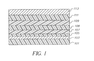
- Figure 1 is a schematic diagram showing a cross-section of a typical organic EL device of the invention containing an interlayer useful in the invention.
- the EL device of the invention is generally as described above. It comprises a compound containing a 3-phenylindolyl group as illustrated in Formula F-1 : wherein R 1 and R 4 represent hydrogen, or an (cyclo)alkyl, or aromatic (carbocyclic or heterocyclic) group and R 2 and R 3 represent hydrogen or one or more optional independently selected substituents on each ring.
- R 1 and R 4 represent hydrogen, or an (cyclo)alkyl, or aromatic (carbocyclic or heterocyclic) group and R 2 and R 3 represent hydrogen or one or more optional independently selected substituents on each ring.
- the compound containing a 3-phenylindolyl group is located in an interlayer (IL) located between a hole-transporting layer and the light emitting layer, and may be in contact with one or both layers.
- the interlayer suitably has a thickness of from 0.1 to 90 nm, typically 0.1 to 25nm and conveniently 0.1 to 15nm.
- the IL will contain a compound represented by Formula F-1 wherein R 2 and R 3 may be independently selected from:
- R 4 is individually selected from Groups 1, 2, 3, and 4; and R 1 is individually selected from Groups 1, 2, 3, 4, and 5.
- the IL contains a compound represented by Formula F-2 : wherein R 4 and R 8 represent a substituent individually selected from Groups 1, 2, 3, and 4; and wherein R 2 , R 3 , R 6 , and R 7 represent one or more substituents on each ring where each substituent is individually selected from the Groups 1 -6 above and Ar is an aromatic group.
- group means any group or atom other than hydrogen.
- substituent group when reference is made in this application to a compound or group that contains a substitutable hydrogen, it is also intended to encompass not only the unsubstituted form, but also its form further substituted with any substituent group or groups as herein mentioned, so long as the substituent does not destroy properties necessary for the intended utility.
- a substituent group may be halogen or may be bonded to the remainder of the molecule by an atom of carbon, silicon, oxygen, nitrogen, phosphorous, or sulfur.
- the substituent may be, for example, halogen, such as chlorine, bromine or fluorine; nitro; hydroxyl; cyano; carboxyl; or groups which may be further substituted, such as alkyl, including straight or branched chain or cyclic alkyl, such as methyl, trifluoromethyl, ethyl, t -butyl, 3-(2,4-di- t -pentylphenoxy) propyl, cyclohexyl, and tetradecyl; alkenyl, such as ethylene, 2-butene; alkoxy, such as methoxy, ethoxy, propoxy, butoxy, 2-methoxyethoxy, sec -butoxy, hexyloxy, 2-ethylhexyloxy, tetradecyloxy, 2-(2,4-di- t -pentylphenoxy)ethoxy, and 2-dodecyloxyethoxy; aryl such as phen
- substituents may themselves be further substituted one or more times with the described substituent groups.
- the particular substituents used may be selected by those skilled in the art to attain the desired desirable properties for a specific application.
- the substituents may be joined together to form a ring such as a fused ring unless otherwise provided.
- the present invention can be employed in most OLED device configurations. These include very simple structures comprising a single anode and cathode to more complex devices, such as passive matrix displays comprised of orthogonal arrays of anodes and cathodes to form pixels, and active-matrix displays where each pixel is controlled independently, for example, with a thin film transistor (TFT).
- TFT thin film transistor
- FIG. 1 A more typical structure is shown in Figure 1 and contains a substrate 101 , an anode 103 , an optional hole-injecting layer 105 , a hole-transporting layer 107 , an interlayer 108 , a light-emitting layer 109 , an electron-transporting layer 111 , and a cathode 113 . These layers are described in detail below. Note that the substrate may alternatively be located adjacent to the cathode, or the substrate may actually constitute the anode or cathode. Also, the total combined thickness of the organic layers is preferably less than 500 nm.
- the substrate 101 can either be light transmissive or opaque, depending on the intended direction of light emission.
- the light transmissive property is desirable for viewing the EL emission through the substrate.
- Transparent glass or organic material are commonly employed in such cases.
- the transmissive characteristic of the bottom support is immaterial, and therefore can be light transmissive, light absorbing or light reflective.
- Substrates for use in this case include, but are not limited to, glass, plastic, semiconductor materials, ceramics, and circuit board materials. Of course it is necessary to provide in these device configurations a light-transparent top electrode.
- the conductive anode layer 103 is commonly formed over the substrate and, when EL emission is viewed through the anode, should be transparent or substantially transparent to the emission of interest.
- Common transparent anode materials used in this invention are indium-tin oxide (ITO) and tin oxide, but other metal oxides can work including, but not limited to, aluminum- or indium-doped zinc oxide (IZO), magnesium-indium oxide, and nickel-tungsten oxide.
- ITO indium-tin oxide
- IZO aluminum- or indium-doped zinc oxide
- IZO aluminum- or indium-doped zinc oxide
- nickel-tungsten oxide nickel-tungsten oxide.
- metal nitrides such as gallium nitride
- metal selenides such as zinc selenide
- metal sulfides such as zinc sulfide
- the transmissive characteristics of layer 103 are immaterial and any conductive material can be used, transparent, opaque or reflective.
- Example conductors for this application include, but are not limited to, gold, iridium, molybdenum, palladium, and platinum.
- Typical anode materials, transmissive or otherwise, have a work function of 4.1 eV or greater. Desired anode materials are commonly deposited by any suitable means such as evaporation, sputtering, chemical vapor deposition, or electrochemical means. Anodes can be patterned using well-known photolithographic processes.
- HIL Hole-Injecting Layer
- a hole-injecting layer 105 be provided between anode 103 and hole-transporting layer 107 .
- the hole-injecting material can serve to improve the film formation property of subsequent organic layers and to facilitate injection of holes into the hole-transporting layer.
- Suitable materials for use in the hole-injecting layer include, but are not limited to, porphyrinic compounds such as those described in US 4,720,432, and plasma-deposited fluorocarbon polymers such as those described in US 6,208,075.
- Alternative hole-injecting materials reportedly useful in organic EL devices are described in EP 0 891 121 A1 and EP 1 029 909 A1.
- HTL Hole-Transporting Layer
- the hole-transporting layer 107 of the organic EL device contains at least one hole-transporting compound such as an aromatic tertiary amine, where the latter is understood to be a compound containing at least one trivalent nitrogen atom that is bonded only to carbon atoms, at least one of which is a member of an aromatic ring.
- the aromatic tertiary amine can be an arylamine, such as a monoarylamine, diarylamine, triarylamine, or a polymeric arylamine group. Exemplary monomeric triarylamines are illustrated by Klupfel et al. US 3,180,730. Other suitable triarylamines substituted with one or more vinyl groups and/or comprising at least one active hydrogen containing group are disclosed by Brantley et al US 3,567,450 and US 3,658,520.
- a more preferred class of aromatic tertiary amines are those which include at least two aromatic tertiary amine moieties as described in US 4,720,432 and US 5,061,569.
- Such compounds include those represented by structural formula (A). wherein Q 1 and Q 2 are independently selected aromatic tertiary amine moieties and G is a linking group such as an arylene, cycloalkylene, or alkylene group of a carbon to carbon bond.
- at least one of Q 1 or Q 2 contains a polycyclic fused ring group, e.g., a naphthalene.
- G is an aryl group, it is conveniently a phenylene, biphenylene, or naphthalene group.
- a useful class of triarylamine groups satisfying structural formula (A) and containing two triarylamine groups is represented by structural formula (B): where R 1 and R 2 each independently represents a hydrogen atom, an aryl group, or an alkyl group or R 1 and R 2 together represent the atoms completing a cycloalkyl group; and R 3 and R 4 each independently represents an aryl group, which is in turn substituted with a diaryl substituted amino group, as indicated by structural formula (C): wherein R 5 and R 6 are independently selected aryl groups.
- at least one of R 5 or R 6 contains a polycyclic fused ring group, e.g., a naphthalene.
- tetraaryldiamines Another class of aromatic tertiary amine groups are the tetraaryldiamines. Desirable tetraaryldiamines groups include two diarylamino groups, such as indicated by formula (C), linked through an arylene group. Useful tetraaryldiamines include those represented by formula (D). wherein each Are is an independently selected arylene group, such as a phenylene or anthracene group, n is an integer of from 1 to 4, and Ar, R 7 , R 8 , and R 9 are independently selected aryl groups. In a typical embodiment, at least one of Ar, R 7 , R 8 , and R 9 is a polycyclic fused ring group, e.g., a naphthalene
- the various alkyl, alkylene, aryl, and arylene groups of the foregoing structural formulae (A), (B), (C), (D), can each in turn be substituted.
- Typical substituents include alkyl groups, alkoxy groups, aryl groups, aryloxy groups, and halogen such as fluoride, chloride, and bromide.
- the various alkyl and alkylene groups typically contain from 1 to 6 carbon atoms.
- the cycloalkyl moieties can contain from 3 to 10 carbon atoms, but typically contain five, six, or seven ring carbon atoms--e.g., cyclopentyl, cyclohexyl, and cycloheptyl ring structures.
- the aryl and arylene groups are usually phenyl and phenylene moieties.
- the hole-transporting layer can be formed of a single or a mixture of aromatic tertiary amine compounds.
- a triarylamine such as a triarylamine satisfying the formula (B)
- a tetraaryldiamine such as indicated by formula (D).
- a triarylamine is employed in combination with a tetraaryldiamine, the latter is positioned as a layer interposed between the triarylamine and the electron injecting and transporting layer.
- useful aromatic tertiary amines are the following:
- Another class of useful hole-transporting materials includes polycyclic aromatic compounds as described in EP 1 009 041.
- polymeric hole-transporting materials can be used such as poly(N-vinylcarbazole) (PVK), polythiophenes, polypyrrole, polyaniline, and copolymers such as poly(3,4-ethylenedioxythiophene) / poly(4-styrenesulfonate) also called PEDOT/PSS.
- the light-emitting layer (LEL) 109 of the organic EL element comprises a luminescent or fluorescent material where electroluminescence is produced as a result of electron-hole pair recombination in this region.
- the light-emitting layer can be comprised of a single material, but more commonly consists of a host material doped with a guest compound or compounds where light emission comes primarily from the dopant and can be of any color.
- the host materials in the light-emitting layer can be an electron-transporting material, as defined below, a hole-transporting material, as defined above, or another material or combination of materials that support hole-electron recombination.
- the dopant is usually chosen from highly fluorescent dyes, but phosphorescent compounds, e.g., transition metal complexes as described in WO 98/55561, WO 00/18851, WO 00/57676, and WO 00/70655 are also useful. Dopants are typically coated as 0.01 to 10 % by weight into the host material.
- Host and emitting molecules known to be of use include, but are not limited to, those disclosed in US 4,768,292, US 5,141,671, US 5,150,006, US 5,151,629, US 5,405,709, US 5,484,922, US 5,593,788, US 5,645,948, US 5,683,823, US 5,755,999, US 5,928,802, US 5,935,720, US 5,935,721, and US 6,020,078.
- Form E Metal complexes of 8-hydroxyquinoline and similar derivatives constitute one class of useful host compounds capable of supporting electroluminescence, and are particularly suitable for light emission of wavelengths longer than 500 nm, e.g., green, yellow, orange, and red.
- M represents a metal
- n is an integer of from 1 to 4
- Z independently in each occurrence represents the atoms completing a nucleus having at least two fused aromatic rings.
- the metal can be monovalent, divalent, trivalent, or tetravalent metal.
- the metal can, for example, be an alkali metal, such as lithium, sodium, or potassium; an alkaline earth metal, such as magnesium or calcium; an earth metal, such aluminum or gallium, or a transition metal such as zinc or zirconium.
- alkali metal such as lithium, sodium, or potassium
- alkaline earth metal such as magnesium or calcium
- earth metal such aluminum or gallium, or a transition metal such as zinc or zirconium.
- any monovalent, divalent, trivalent, or tetravalent metal known to be a useful chelating metal can be employed.
- Z completes a heterocyclic nucleus containing at least two fused aromatic rings, at least one of which is an azole or azine ring. Additional rings, including both aliphatic and aromatic rings, can be fused with the two required rings, if required. To avoid adding molecular bulk without improving on function the number of ring atoms is usually maintained at 18 or less.
- Illustrative of useful chelated oxinoid compounds are the following:
- Formula F Derivatives of 9,10-di-(2-naphthyl)anthracene (Formula F) constitute one class of useful hosts capable of supporting electroluminescence, and are particularly suitable for light emission of wavelengths longer than 400 nm, e.g., blue, green, yellow, orange or red.
- R 1 , R 2 , R 3 , R 4 , R 5 , and R 6 represent hydrogen or one or more substituents selected from the following groups:
- Illustrative examples include 9,10-di-(2-naphthyl)anthracene and 2- t -butyl-9,10-di-(2-naphthyl)anthracene.
- Other anthracene derivatives can be useful as a host in the LEL, including derivatives of 9,10-bis[4-(2,2-diphenylethenyl)phenyl]anthracene.
- Benzazole derivatives constitute another class of useful hosts capable of supporting electroluminescence, and are particularly suitable for light emission of wavelengths longer than 400 nm, e.g., blue, green, yellow, orange or red.
- n is an integer of 3 to 8
- Z is -O, -NR or -S where R is H or a substituent
- R' represents one or more optional substituents where R and each R' are H or alkyl groups such as propyl, t-butyl, and heptyl groups typically having from 1 to 24 carbon atoms; carbocyclic or heterocyclic ring groups such as phenyl and naphthyl, furyl, thienyl, pyridyl, and quinolinyl groups and atoms necessary to complete a fused aromatic ring group typically having from 5 to 20 carbon atoms; and halo such as chloro, and fluoro;
- L is a linkage unit usually comprising an alkyl or aryl group
- An example of a useful benzazole is 2, 2', 2"-(1,3,5-phenylene)tris[1-phenyl-1H-benzimidazole].
- Desirable fluorescent dopants include groups derived from fused ring, heterocyclic and other compounds such as anthracene, tetracene, xanthene, perylene, rubrene, coumarin, rhodamine, quinacridone, dicyanomethylenepyran, thiopyran , polymethine, pyrilium thiapyrilium, and carbostyryl compounds.
- useful dopants include, but are not limited to, the following:
- ETL Electron-Transporting Layer
- Preferred thin film-forming materials for use in forming the electron-transporting layer 111 of the organic EL devices of this invention are metal chelated oxinoid compounds, including chelates of oxine itself (also commonly referred to as 8-quinolinol or 8-hydroxyquinoline). Such compounds help to inject and transport electrons and exhibit both high levels of performance and are readily fabricated in the form of thin films.
- exemplary of contemplated oxinoid compounds are those satisfying structural formula (E), previously described.
- electron-transporting materials include various butadiene derivatives as disclosed in US 4,356,429 and various heterocyclic optical brighteners as described in US 4,539,507. Benzazoles satisfying structural formula (G) are also useful electron transporting materials.
- layers 109 and 111 can optionally be collapsed into a single layer that serves the function of supporting both light emission and electron transportation.
- the cathode layer 113 used in this invention can be comprised of nearly any conductive material. Desirable materials have good film-forming properties to ensure good contact with the underlying organic layer, promote electron injection at low voltage, and have good stability. Useful cathode materials often contain a low work function metal ( ⁇ 4.0 eV) or metal alloy. One preferred cathode material is comprised of a Mg:Ag alloy wherein the percentage of silver is in the range of 1 to 20 %, as described in US 4,885,221. Another suitable class of cathode materials includes bilayers comprised of a thin layer of a low work function metal or metal salt capped with a thicker layer of conductive metal.
- cathode is comprised of a thin layer of LiF followed by a thicker layer of A1 as described in US 5,677,572.
- Other useful cathode materials include, but are not limited to, those disclosed in US 5,059,861, US 5,059,862, and US 6,140,763.
- cathode When light emission is viewed through the cathode, the cathode must be transparent or nearly transparent. For such applications, metals must be thin or one must use transparent conductive oxides, or a combination of these materials.
- Optically transparent cathodes have been described in more detail in US 5,776,623. Cathode materials can be deposited by evaporation, sputtering, or chemical vapor deposition. When needed, patterning can be achieved through many well known methods including, but not limited to, through-mask deposition, integral shadow masking as described in US 5,276,380 and EP 0 732 868, laser ablation, and selective chemical vapor deposition.
- the organic materials mentioned above are suitably deposited through sublimation, but can be deposited from a solvent with an optional binder to improve film formation. If the material is a polymer, solvent deposition is usually preferred.
- the material to be deposited by sublimation can be vaporized from a sublimator "boat" often comprised of a tantalum material, e.g., as described in US 6,237,529, or can be first coated onto a donor sheet and then sublimed in closer proximity to the substrate. Layers with a mixture of materials can utilize separate sublimator boats or the materials can be pre-mixed and coated from a single boat or donor sheet.
- Patterned deposition can be achieved using shadow masks, integral shadow masks (US 5,294,870), spatially-defined thermal dye transfer from a donor sheet (US 5,851,709 and US 6,066,357) and inkjet method (US 6,066,357).
- OLED devices are sensitive to moisture and/or oxygen so they are commonly sealed in an inert atmosphere such as nitrogen or argon, along with a desiccant such as alumina, bauxite, calcium sulfate, clays, silica gel, zeolites, alkaline metal oxides, alkaline earth metal oxides, sulfates, or metal halides and perchlorates.
- a desiccant such as alumina, bauxite, calcium sulfate, clays, silica gel, zeolites, alkaline metal oxides, alkaline earth metal oxides, sulfates, or metal halides and perchlorates.
- Titanium trichloride (0.43g, 2.81mmol), zinc (9.2g, 14mmol), and trimethylsilyl chloride (17.8mL, 14mmol) was added to a mixture of amide S-1 (7.0g, 9.36mmol) in 1,2-dimethoxyethane (93mL). The mixture was heated to 110°C for 8 hours, then cooled to room temperature. The mixture was filtered through a pad of silica gel with methylene chloride. The filtrate was concentrated with a rotary evaporator and recrystallized from ethyl acetate and heptane to yield S-2.
- a series of EL devices satisfying the requirements of the invention were constructed in the following manner: A glass substrate coated with an 42 nm layer of indium-tin oxide (ITO) as the anode was sequentially ultrasonicated in a commercial detergent, rinsed in deionized water, degreased in toluene vapor and exposed to oxygen plasma for about 1 min.
- ITO indium-tin oxide
- a comparison device was prepared omitting layer c) and containing an overall device layer thickness substantially the same as the other examples.
- the inventive samples provide an improved luminance over the corresponding comparison samples.
- Sample 3-1 represents a HTL of NPB only and Sample 3-7 represents a HTL containing I-1 only. It is noted that the use of I-1 in the HTL improves the luminance vs. NPB, but at an extreme penalty for voltage requires.
- the inventive devices exhibit improved relative luminance with little or no increase in voltage requirement.
- Embodiments of the invention include the device where where: the IL is between 0.1 and 90nm or desirably between 0.1 and 15nm thick; the HTL contains an aromatic tertiary amine group containing at least one trivalent nitrogen atom that is bonded only to carbon atoms, at least one of which is a member of an aromatic ring group; the LEL contains a dopant in an amount of 0.01 to 20% by weight; the ETL contains tris(8-quinolinolato)aluminum(III); the LEL contains a compound having formula I: wherein M represents a metal; n is an integer of from 1 to 3; and Z independently in each occurrence represents the atoms completing a nucleus having at least two fused aromatic rings; the LEL contains a compound that fluoresces with the color red; R 1 in formula F-1 is an aromatic group of from 5 to 20 carbon atoms such as one represented by Formula II: wherein R 5 represents one or more substituents on the aromatic ring where each is independently selected
- R 4 and R 8 are independently selected from Groups 1, 2, 3, and 4 as above,
- Ar is a para-substituted phenyl group such as a 4,4'-substituted biphenyl group or a 1,3,5-trisubstituted phenyl group, wherein each of the substituents is a 3-phenylindolyl group; the compound containing a 3-phenylindolyl group contains at least two 3-phenylindolyl groups; and includes a static or motion imaging device incorporating the device of the invention.
Landscapes
- Chemical & Material Sciences (AREA)
- Engineering & Computer Science (AREA)
- Materials Engineering (AREA)
- Organic Chemistry (AREA)
- Physics & Mathematics (AREA)
- Spectroscopy & Molecular Physics (AREA)
- Electroluminescent Light Sources (AREA)
Applications Claiming Priority (2)
| Application Number | Priority Date | Filing Date | Title |
|---|---|---|---|
| US83031 | 2002-02-26 | ||
| US10/083,031 US6670053B2 (en) | 2002-02-26 | 2002-02-26 | Organic electroluminescent devices with high luminance |
Publications (2)
| Publication Number | Publication Date |
|---|---|
| EP1339264A2 true EP1339264A2 (de) | 2003-08-27 |
| EP1339264A3 EP1339264A3 (de) | 2006-11-15 |
Family
ID=27660375
Family Applications (1)
| Application Number | Title | Priority Date | Filing Date |
|---|---|---|---|
| EP03075428A Withdrawn EP1339264A3 (de) | 2002-02-26 | 2003-02-14 | Organische elektrolumineszente Vorrichtungen mit hoher Lichtausbeute |
Country Status (6)
| Country | Link |
|---|---|
| US (1) | US6670053B2 (de) |
| EP (1) | EP1339264A3 (de) |
| JP (1) | JP2003282271A (de) |
| KR (1) | KR20030070846A (de) |
| CN (1) | CN1441628A (de) |
| TW (1) | TW200303702A (de) |
Cited By (7)
| Publication number | Priority date | Publication date | Assignee | Title |
|---|---|---|---|---|
| WO2005056713A1 (en) * | 2003-12-05 | 2005-06-23 | Eastman Kodak Company | Organic element for electroluminescent devices |
| WO2005080527A1 (en) * | 2004-02-17 | 2005-09-01 | Eastman Kodak Company | Anthracene derivative host having ranges of dopants |
| WO2005096401A3 (en) * | 2004-03-30 | 2005-11-10 | Osram Opto Semiconductors Gmbh | Device structure to improve oled reliability |
| EP1653529A1 (de) * | 2004-10-11 | 2006-05-03 | Samsung SDI Co., Ltd. | Organische elektrolumineszierende Vorrichtung und deren Herstellungsmethode |
| WO2008123540A3 (en) * | 2007-03-30 | 2008-12-24 | Fujifilm Corp | Organic electroluminescent device |
| EP2241563A4 (de) * | 2008-01-25 | 2011-06-08 | Univ Keio | Tri-substituierte aromatische verbindung |
| US8018144B2 (en) | 2008-02-26 | 2011-09-13 | Samsung Mobile Display Co., Ltd. | Organic light emitting diode and method of fabricating the same |
Families Citing this family (16)
| Publication number | Priority date | Publication date | Assignee | Title |
|---|---|---|---|---|
| US6790539B2 (en) * | 2002-07-19 | 2004-09-14 | Lightronik Technology Inc. | Organic electroluminescence element |
| JP3706605B2 (ja) * | 2002-09-27 | 2005-10-12 | 三洋電機株式会社 | 有機エレクトロルミネッセンス素子およびその製造方法 |
| US7232617B2 (en) * | 2003-02-04 | 2007-06-19 | Cityu Research Limited | Electroluminescent devices |
| US7326371B2 (en) * | 2004-03-25 | 2008-02-05 | Eastman Kodak Company | Electroluminescent device with anthracene derivative host |
| CN100384835C (zh) * | 2004-04-16 | 2008-04-30 | 中国科学院上海有机化学研究所 | 双吲哚杂环类化合物及其制备方法和用于有机电致发光材料的用途 |
| US7300731B2 (en) * | 2004-08-10 | 2007-11-27 | E.I. Du Pont De Nemours And Company | Spatially-doped charge transport layers |
| KR101030008B1 (ko) * | 2004-12-31 | 2011-04-20 | 삼성모바일디스플레이주식회사 | 유기 전계 발광 소자 |
| KR100696505B1 (ko) * | 2005-03-31 | 2007-03-19 | 삼성에스디아이 주식회사 | 유기 전계 발광 소자 및 그 제조방법 |
| US7622619B2 (en) * | 2005-07-20 | 2009-11-24 | Lg Display Co., Ltd. | Synthesis process |
| KR100881455B1 (ko) * | 2006-08-14 | 2009-02-06 | 주식회사 잉크테크 | 유기전계발광소자 및 이의 제조방법 |
| JP5282260B2 (ja) * | 2006-11-27 | 2013-09-04 | ユー・ディー・シー アイルランド リミテッド | 有機電界発光素子 |
| JP5187493B2 (ja) * | 2006-11-27 | 2013-04-24 | ユー・ディー・シー アイルランド リミテッド | 有機電界発光素子および新規なインドール誘導体 |
| KR100858816B1 (ko) * | 2007-03-14 | 2008-09-17 | 삼성에스디아이 주식회사 | 안트라센 유도체 화합물을 포함하는 유기막을 구비하는유기 발광 소자 |
| KR20090082778A (ko) * | 2008-01-28 | 2009-07-31 | 삼성모바일디스플레이주식회사 | 유기전계발광소자 및 그 제조방법 |
| KR100858826B1 (ko) | 2008-06-30 | 2008-09-17 | 삼성에스디아이 주식회사 | 안트라센 유도체 화합물을 포함하는 유기막을 구비하는유기 발광 소자 |
| CN114695715A (zh) * | 2020-12-31 | 2022-07-01 | Tcl科技集团股份有限公司 | 一种量子点发光二极管及其制备方法 |
Family Cites Families (7)
| Publication number | Priority date | Publication date | Assignee | Title |
|---|---|---|---|---|
| DE2204725B2 (de) * | 1971-02-02 | 1974-02-07 | Ciba-Geigy Ag, Basel (Schweiz) | Verfahren zur Herstellung von konzentrierten, flüssigen, salzarmen Färbepräparaten |
| JP3229654B2 (ja) | 1992-06-05 | 2001-11-19 | ティーディーケイ株式会社 | 有機el素子用化合物および有機el素子 |
| US5766779A (en) * | 1996-08-20 | 1998-06-16 | Eastman Kodak Company | Electron transporting materials for organic electroluminescent devices |
| JP3470631B2 (ja) * | 1999-03-01 | 2003-11-25 | 富士電機株式会社 | 蛍光変換フィルターの製造方法および有機el素子 |
| JP2001118683A (ja) | 1999-08-12 | 2001-04-27 | Toray Ind Inc | 発光素子 |
| JP4590678B2 (ja) * | 2000-04-05 | 2010-12-01 | 東レ株式会社 | 発光素子 |
| US6693295B2 (en) * | 2000-12-25 | 2004-02-17 | Fuji Photo Film Co., Ltd. | Indole derivative, material for light-emitting device and light-emitting device using the same |
-
2002
- 2002-02-26 US US10/083,031 patent/US6670053B2/en not_active Expired - Lifetime
- 2002-12-31 TW TW091138028A patent/TW200303702A/zh unknown
-
2003
- 2003-02-14 EP EP03075428A patent/EP1339264A3/de not_active Withdrawn
- 2003-02-25 KR KR10-2003-0011702A patent/KR20030070846A/ko not_active Withdrawn
- 2003-02-26 CN CN03106614A patent/CN1441628A/zh active Pending
- 2003-02-26 JP JP2003048901A patent/JP2003282271A/ja active Pending
Cited By (12)
| Publication number | Priority date | Publication date | Assignee | Title |
|---|---|---|---|---|
| WO2005056713A1 (en) * | 2003-12-05 | 2005-06-23 | Eastman Kodak Company | Organic element for electroluminescent devices |
| US7090930B2 (en) | 2003-12-05 | 2006-08-15 | Eastman Kodak Company | Organic element for electroluminescent devices |
| WO2005080527A1 (en) * | 2004-02-17 | 2005-09-01 | Eastman Kodak Company | Anthracene derivative host having ranges of dopants |
| US7252893B2 (en) | 2004-02-17 | 2007-08-07 | Eastman Kodak Company | Anthracene derivative host having ranges of dopants |
| WO2005096401A3 (en) * | 2004-03-30 | 2005-11-10 | Osram Opto Semiconductors Gmbh | Device structure to improve oled reliability |
| EP1653529A1 (de) * | 2004-10-11 | 2006-05-03 | Samsung SDI Co., Ltd. | Organische elektrolumineszierende Vorrichtung und deren Herstellungsmethode |
| US7811680B2 (en) | 2004-10-11 | 2010-10-12 | Samsung Mobile Display Co., Ltd. | Organic EL device and method of manufacturing the same |
| WO2008123540A3 (en) * | 2007-03-30 | 2008-12-24 | Fujifilm Corp | Organic electroluminescent device |
| US8890122B2 (en) | 2007-03-30 | 2014-11-18 | Udc Ireland Limited | Organic electroluminescent device |
| US9472769B2 (en) | 2007-03-30 | 2016-10-18 | Udc Ireland Limited | Organic electroluminescent device |
| EP2241563A4 (de) * | 2008-01-25 | 2011-06-08 | Univ Keio | Tri-substituierte aromatische verbindung |
| US8018144B2 (en) | 2008-02-26 | 2011-09-13 | Samsung Mobile Display Co., Ltd. | Organic light emitting diode and method of fabricating the same |
Also Published As
| Publication number | Publication date |
|---|---|
| US20030180573A1 (en) | 2003-09-25 |
| JP2003282271A (ja) | 2003-10-03 |
| KR20030070846A (ko) | 2003-09-02 |
| CN1441628A (zh) | 2003-09-10 |
| TW200303702A (en) | 2003-09-01 |
| EP1339264A3 (de) | 2006-11-15 |
| US6670053B2 (en) | 2003-12-30 |
Similar Documents
| Publication | Publication Date | Title |
|---|---|---|
| US6661023B2 (en) | Organic element for electroluminescent devices | |
| US6824893B2 (en) | Organic element for electroluminescent devices | |
| US6670053B2 (en) | Organic electroluminescent devices with high luminance | |
| US6841267B2 (en) | Efficient electroluminescent device | |
| US20050271899A1 (en) | Efficient electroluminescent device | |
| US6849345B2 (en) | Organic electroluminescent devices with high luminance | |
| US20060204783A1 (en) | Organic electroluminescent device | |
| US7662485B2 (en) | White organic light-emitting devices with improved performance | |
| US20060204784A1 (en) | Organic light-emitting devices with mixed electron transport materials | |
| US20060088729A1 (en) | White organic light-emitting devices with improved performance | |
| US7264889B2 (en) | Stable electroluminescent device | |
| US7517595B2 (en) | Electroluminescent devices with mixed electron transport materials | |
| US7329466B2 (en) | Organic element for electroluminescent devices | |
| US7052785B2 (en) | Organic element for electroluminescent devices | |
| EP1973984A1 (de) | Elektrolumineszenzvorrichtung mit einem galliumkomplex | |
| US7083865B2 (en) | Organic element for electroluminescent devices | |
| US7087320B2 (en) | Organic element for electroluminescent devices | |
| US20060088730A1 (en) | Organic light-emitting devices with improved performance | |
| US7049012B2 (en) | Organic element for electroluminescent devices | |
| US20050214567A1 (en) | Organic element for electroluminescent devices |
Legal Events
| Date | Code | Title | Description |
|---|---|---|---|
| PUAI | Public reference made under article 153(3) epc to a published international application that has entered the european phase |
Free format text: ORIGINAL CODE: 0009012 |
|
| AK | Designated contracting states |
Designated state(s): AT BE BG CH CY CZ DE DK EE ES FI FR GB GR HU IE IT LI LU MC NL PT SE SI SK TR |
|
| AX | Request for extension of the european patent |
Extension state: AL LT LV MK RO |
|
| PUAL | Search report despatched |
Free format text: ORIGINAL CODE: 0009013 |
|
| AK | Designated contracting states |
Kind code of ref document: A3 Designated state(s): AT BE BG CH CY CZ DE DK EE ES FI FR GB GR HU IE IT LI LU MC NL PT SE SI SK TR |
|
| AX | Request for extension of the european patent |
Extension state: AL LT LV MK RO |
|
| STAA | Information on the status of an ep patent application or granted ep patent |
Free format text: STATUS: THE APPLICATION IS DEEMED TO BE WITHDRAWN |
|
| 18D | Application deemed to be withdrawn |
Effective date: 20060901 |