JP5713686B2 - Organic compound, organic light emitting device and image display device - Google Patents
Organic compound, organic light emitting device and image display device Download PDFInfo
- Publication number
- JP5713686B2 JP5713686B2 JP2011002263A JP2011002263A JP5713686B2 JP 5713686 B2 JP5713686 B2 JP 5713686B2 JP 2011002263 A JP2011002263 A JP 2011002263A JP 2011002263 A JP2011002263 A JP 2011002263A JP 5713686 B2 JP5713686 B2 JP 5713686B2
- Authority
- JP
- Japan
- Prior art keywords
- group
- light emitting
- organic compound
- organic
- compound
- Prior art date
- Legal status (The legal status is an assumption and is not a legal conclusion. Google has not performed a legal analysis and makes no representation as to the accuracy of the status listed.)
- Active
Links
- 150000002894 organic compounds Chemical class 0.000 title claims description 97
- 125000003118 aryl group Chemical group 0.000 claims description 34
- HEDRZPFGACZZDS-UHFFFAOYSA-N Chloroform Chemical compound ClC(Cl)Cl HEDRZPFGACZZDS-UHFFFAOYSA-N 0.000 claims description 28
- 125000001424 substituent group Chemical group 0.000 claims description 26
- 125000000217 alkyl group Chemical group 0.000 claims description 18
- 125000004435 hydrogen atom Chemical group [H]* 0.000 claims description 13
- 125000003545 alkoxy group Chemical group 0.000 claims description 11
- 125000003277 amino group Chemical group 0.000 claims description 11
- 125000005843 halogen group Chemical group 0.000 claims description 11
- 125000000623 heterocyclic group Chemical group 0.000 claims description 11
- 125000004104 aryloxy group Chemical group 0.000 claims description 9
- 125000000484 butyl group Chemical group [H]C([*])([H])C([H])([H])C([H])([H])C([H])([H])[H] 0.000 claims description 9
- 125000003710 aryl alkyl group Chemical group 0.000 claims description 8
- 125000004093 cyano group Chemical group *C#N 0.000 claims description 8
- 125000005412 pyrazyl group Chemical group 0.000 claims description 6
- 125000000714 pyrimidinyl group Chemical group 0.000 claims description 6
- 229910052731 fluorine Inorganic materials 0.000 claims description 4
- 125000002102 aryl alkyloxo group Chemical group 0.000 claims description 2
- 125000001153 fluoro group Chemical group F* 0.000 claims description 2
- 125000004432 carbon atom Chemical group C* 0.000 claims 2
- 150000001875 compounds Chemical class 0.000 description 130
- 239000010410 layer Substances 0.000 description 92
- YXFVVABEGXRONW-UHFFFAOYSA-N Toluene Chemical compound CC1=CC=CC=C1 YXFVVABEGXRONW-UHFFFAOYSA-N 0.000 description 30
- 239000000243 solution Substances 0.000 description 29
- -1 1-adamantyl group Chemical group 0.000 description 27
- 239000000463 material Substances 0.000 description 27
- 238000006243 chemical reaction Methods 0.000 description 26
- 230000015572 biosynthetic process Effects 0.000 description 17
- 239000000758 substrate Substances 0.000 description 17
- 238000003786 synthesis reaction Methods 0.000 description 17
- 238000000034 method Methods 0.000 description 16
- OKKJLVBELUTLKV-UHFFFAOYSA-N Methanol Chemical compound OC OKKJLVBELUTLKV-UHFFFAOYSA-N 0.000 description 12
- 238000000295 emission spectrum Methods 0.000 description 12
- 239000010408 film Substances 0.000 description 12
- 238000002347 injection Methods 0.000 description 12
- 239000007924 injection Substances 0.000 description 12
- 238000000859 sublimation Methods 0.000 description 12
- 230000008022 sublimation Effects 0.000 description 12
- 239000002904 solvent Substances 0.000 description 11
- KFZMGEQAYNKOFK-UHFFFAOYSA-N Isopropanol Chemical compound CC(C)O KFZMGEQAYNKOFK-UHFFFAOYSA-N 0.000 description 9
- LFQSCWFLJHTTHZ-UHFFFAOYSA-N Ethanol Chemical compound CCO LFQSCWFLJHTTHZ-UHFFFAOYSA-N 0.000 description 8
- IMNFDUFMRHMDMM-UHFFFAOYSA-N N-Heptane Chemical compound CCCCCCC IMNFDUFMRHMDMM-UHFFFAOYSA-N 0.000 description 8
- 230000005525 hole transport Effects 0.000 description 8
- 230000003647 oxidation Effects 0.000 description 8
- 238000007254 oxidation reaction Methods 0.000 description 8
- 230000000903 blocking effect Effects 0.000 description 7
- 238000010438 heat treatment Methods 0.000 description 7
- 229910052751 metal Inorganic materials 0.000 description 7
- 239000002184 metal Substances 0.000 description 7
- HEMHJVSKTPXQMS-UHFFFAOYSA-M Sodium hydroxide Chemical compound [OH-].[Na+] HEMHJVSKTPXQMS-UHFFFAOYSA-M 0.000 description 6
- 239000003153 chemical reaction reagent Substances 0.000 description 6
- 238000004128 high performance liquid chromatography Methods 0.000 description 6
- 238000005259 measurement Methods 0.000 description 6
- 238000006862 quantum yield reaction Methods 0.000 description 6
- 239000002356 single layer Substances 0.000 description 6
- 239000007787 solid Substances 0.000 description 6
- 239000000470 constituent Substances 0.000 description 5
- 230000005284 excitation Effects 0.000 description 5
- 238000004768 lowest unoccupied molecular orbital Methods 0.000 description 5
- 125000001624 naphthyl group Chemical group 0.000 description 5
- 125000001997 phenyl group Chemical group [H]C1=C([H])C([H])=C(*)C([H])=C1[H] 0.000 description 5
- 238000001771 vacuum deposition Methods 0.000 description 5
- GQHTUMJGOHRCHB-UHFFFAOYSA-N 2,3,4,6,7,8,9,10-octahydropyrimido[1,2-a]azepine Chemical compound C1CCCCN2CCCN=C21 GQHTUMJGOHRCHB-UHFFFAOYSA-N 0.000 description 4
- 238000004440 column chromatography Methods 0.000 description 4
- 238000001816 cooling Methods 0.000 description 4
- 239000011521 glass Substances 0.000 description 4
- 125000005842 heteroatom Chemical group 0.000 description 4
- 150000002739 metals Chemical class 0.000 description 4
- 239000002244 precipitate Substances 0.000 description 4
- 239000011347 resin Substances 0.000 description 4
- 229920005989 resin Polymers 0.000 description 4
- 238000004544 sputter deposition Methods 0.000 description 4
- 239000011230 binding agent Substances 0.000 description 3
- 238000000576 coating method Methods 0.000 description 3
- 239000007772 electrode material Substances 0.000 description 3
- 125000003983 fluorenyl group Chemical group C1(=CC=CC=2C3=CC=CC=C3CC12)* 0.000 description 3
- 238000004770 highest occupied molecular orbital Methods 0.000 description 3
- 229930195733 hydrocarbon Natural products 0.000 description 3
- 150000002430 hydrocarbons Chemical class 0.000 description 3
- 230000009878 intermolecular interaction Effects 0.000 description 3
- 238000000059 patterning Methods 0.000 description 3
- 238000009751 slip forming Methods 0.000 description 3
- UKSZBOKPHAQOMP-SVLSSHOZSA-N (1e,4e)-1,5-diphenylpenta-1,4-dien-3-one;palladium Chemical compound [Pd].C=1C=CC=CC=1\C=C\C(=O)\C=C\C1=CC=CC=C1.C=1C=CC=CC=1\C=C\C(=O)\C=C\C1=CC=CC=C1 UKSZBOKPHAQOMP-SVLSSHOZSA-N 0.000 description 2
- CSCPPACGZOOCGX-UHFFFAOYSA-N Acetone Chemical compound CC(C)=O CSCPPACGZOOCGX-UHFFFAOYSA-N 0.000 description 2
- WKBOTKDWSSQWDR-UHFFFAOYSA-N Bromine atom Chemical compound [Br] WKBOTKDWSSQWDR-UHFFFAOYSA-N 0.000 description 2
- ZAMOUSCENKQFHK-UHFFFAOYSA-N Chlorine atom Chemical compound [Cl] ZAMOUSCENKQFHK-UHFFFAOYSA-N 0.000 description 2
- PXGOKWXKJXAPGV-UHFFFAOYSA-N Fluorine Chemical compound FF PXGOKWXKJXAPGV-UHFFFAOYSA-N 0.000 description 2
- PXHVJJICTQNCMI-UHFFFAOYSA-N Nickel Chemical compound [Ni] PXHVJJICTQNCMI-UHFFFAOYSA-N 0.000 description 2
- CTQNGGLPUBDAKN-UHFFFAOYSA-N O-Xylene Chemical compound CC1=CC=CC=C1C CTQNGGLPUBDAKN-UHFFFAOYSA-N 0.000 description 2
- KDLHZDBZIXYQEI-UHFFFAOYSA-N Palladium Chemical compound [Pd] KDLHZDBZIXYQEI-UHFFFAOYSA-N 0.000 description 2
- XLOMVQKBTHCTTD-UHFFFAOYSA-N Zinc monoxide Chemical compound [Zn]=O XLOMVQKBTHCTTD-UHFFFAOYSA-N 0.000 description 2
- 229910045601 alloy Inorganic materials 0.000 description 2
- 239000000956 alloy Substances 0.000 description 2
- MWPLVEDNUUSJAV-UHFFFAOYSA-N anthracene Chemical compound C1=CC=CC2=CC3=CC=CC=C3C=C21 MWPLVEDNUUSJAV-UHFFFAOYSA-N 0.000 description 2
- 229940027991 antiseptic and disinfectant quinoline derivative Drugs 0.000 description 2
- 125000006267 biphenyl group Chemical group 0.000 description 2
- GDTBXPJZTBHREO-UHFFFAOYSA-N bromine Substances BrBr GDTBXPJZTBHREO-UHFFFAOYSA-N 0.000 description 2
- 229910052794 bromium Inorganic materials 0.000 description 2
- 239000000460 chlorine Substances 0.000 description 2
- 229910052801 chlorine Inorganic materials 0.000 description 2
- 229920001940 conductive polymer Polymers 0.000 description 2
- 239000013078 crystal Substances 0.000 description 2
- 238000000151 deposition Methods 0.000 description 2
- 125000001301 ethoxy group Chemical group [H]C([H])([H])C([H])([H])O* 0.000 description 2
- 125000001495 ethyl group Chemical group [H]C([H])([H])C([H])([H])* 0.000 description 2
- 238000011156 evaluation Methods 0.000 description 2
- 238000001914 filtration Methods 0.000 description 2
- 239000011737 fluorine Substances 0.000 description 2
- AMGQUBHHOARCQH-UHFFFAOYSA-N indium;oxotin Chemical compound [In].[Sn]=O AMGQUBHHOARCQH-UHFFFAOYSA-N 0.000 description 2
- OWFXIOWLTKNBAP-UHFFFAOYSA-N isoamyl nitrite Chemical compound CC(C)CCON=O OWFXIOWLTKNBAP-UHFFFAOYSA-N 0.000 description 2
- 125000001449 isopropyl group Chemical group [H]C([H])([H])C([H])(*)C([H])([H])[H] 0.000 description 2
- 239000007788 liquid Substances 0.000 description 2
- 229910044991 metal oxide Inorganic materials 0.000 description 2
- 150000004706 metal oxides Chemical class 0.000 description 2
- 125000000956 methoxy group Chemical group [H]C([H])([H])O* 0.000 description 2
- 125000002496 methyl group Chemical group [H]C([H])([H])* 0.000 description 2
- 229910052757 nitrogen Inorganic materials 0.000 description 2
- 125000002080 perylenyl group Chemical group C1(=CC=C2C=CC=C3C4=CC=CC5=CC=CC(C1=C23)=C45)* 0.000 description 2
- 125000000951 phenoxy group Chemical group [H]C1=C([H])C([H])=C(O*)C([H])=C1[H] 0.000 description 2
- BASFCYQUMIYNBI-UHFFFAOYSA-N platinum Chemical compound [Pt] BASFCYQUMIYNBI-UHFFFAOYSA-N 0.000 description 2
- 229920003227 poly(N-vinyl carbazole) Polymers 0.000 description 2
- 229920000123 polythiophene Polymers 0.000 description 2
- 125000002572 propoxy group Chemical group [*]OC([H])([H])C(C([H])([H])[H])([H])[H] 0.000 description 2
- 239000011241 protective layer Substances 0.000 description 2
- 125000005581 pyrene group Chemical group 0.000 description 2
- 125000004076 pyridyl group Chemical group 0.000 description 2
- 150000003248 quinolines Chemical class 0.000 description 2
- 150000003252 quinoxalines Chemical class 0.000 description 2
- 239000004065 semiconductor Substances 0.000 description 2
- 229910052709 silver Inorganic materials 0.000 description 2
- 239000004332 silver Substances 0.000 description 2
- 230000002194 synthesizing effect Effects 0.000 description 2
- 239000010409 thin film Substances 0.000 description 2
- 125000005259 triarylamine group Chemical group 0.000 description 2
- WLPUWLXVBWGYMZ-UHFFFAOYSA-N tricyclohexylphosphine Chemical compound C1CCCCC1P(C1CCCCC1)C1CCCCC1 WLPUWLXVBWGYMZ-UHFFFAOYSA-N 0.000 description 2
- XLYOFNOQVPJJNP-UHFFFAOYSA-N water Substances O XLYOFNOQVPJJNP-UHFFFAOYSA-N 0.000 description 2
- 239000008096 xylene Substances 0.000 description 2
- YJTKZCDBKVTVBY-UHFFFAOYSA-N 1,3-Diphenylbenzene Chemical group C1=CC=CC=C1C1=CC=CC(C=2C=CC=CC=2)=C1 YJTKZCDBKVTVBY-UHFFFAOYSA-N 0.000 description 1
- ZCYVEMRRCGMTRW-UHFFFAOYSA-N 7553-56-2 Chemical compound [I] ZCYVEMRRCGMTRW-UHFFFAOYSA-N 0.000 description 1
- 229920000178 Acrylic resin Polymers 0.000 description 1
- 239000004925 Acrylic resin Substances 0.000 description 1
- 229910000838 Al alloy Inorganic materials 0.000 description 1
- 229910001148 Al-Li alloy Inorganic materials 0.000 description 1
- YERIUYIANLAXEL-UHFFFAOYSA-N BrC(C1)C(Br)=Cc2c1c(-c1ccccc1)c(-c1ccc-3c4c1c-1ccc4-c4c5c-3cccc5ccc4)c-1c2-c1ccccc1 Chemical compound BrC(C1)C(Br)=Cc2c1c(-c1ccccc1)c(-c1ccc-3c4c1c-1ccc4-c4c5c-3cccc5ccc4)c-1c2-c1ccccc1 YERIUYIANLAXEL-UHFFFAOYSA-N 0.000 description 1
- NWPSDRPTCVEYTD-UHFFFAOYSA-N Brc(c(Br)c1)cc2c1c(-c1ccccc1)c(-c1ccc-3c4c1c-1ccc4-c4c5c-3cccc5ccc4)c-1c2-c1ccccc1 Chemical compound Brc(c(Br)c1)cc2c1c(-c1ccccc1)c(-c1ccc-3c4c1c-1ccc4-c4c5c-3cccc5ccc4)c-1c2-c1ccccc1 NWPSDRPTCVEYTD-UHFFFAOYSA-N 0.000 description 1
- FPLWLPDDQWOVNN-UHFFFAOYSA-N C(C(c1cccc2c1c1ccc2)C1=Cc1c(c(-c(cc2)c34)c5-c3ccc-3c4c2-c2c4c-3cccc4ccc2)-c2ccccc2)c1c5-c1ccccc1 Chemical compound C(C(c1cccc2c1c1ccc2)C1=Cc1c(c(-c(cc2)c34)c5-c3ccc-3c4c2-c2c4c-3cccc4ccc2)-c2ccccc2)c1c5-c1ccccc1 FPLWLPDDQWOVNN-UHFFFAOYSA-N 0.000 description 1
- WQGRAXGAXSNSDL-UHFFFAOYSA-N CC1(C)OB(c2c(cccc3)c3ccc2)OC1(C)C Chemical compound CC1(C)OB(c2c(cccc3)c3ccc2)OC1(C)C WQGRAXGAXSNSDL-UHFFFAOYSA-N 0.000 description 1
- OYPRJOBELJOOCE-UHFFFAOYSA-N Calcium Chemical compound [Ca] OYPRJOBELJOOCE-UHFFFAOYSA-N 0.000 description 1
- VYZAMTAEIAYCRO-UHFFFAOYSA-N Chromium Chemical compound [Cr] VYZAMTAEIAYCRO-UHFFFAOYSA-N 0.000 description 1
- RYGMFSIKBFXOCR-UHFFFAOYSA-N Copper Chemical compound [Cu] RYGMFSIKBFXOCR-UHFFFAOYSA-N 0.000 description 1
- WHXSMMKQMYFTQS-UHFFFAOYSA-N Lithium Chemical compound [Li] WHXSMMKQMYFTQS-UHFFFAOYSA-N 0.000 description 1
- RJQGTUPMSDNELX-UHFFFAOYSA-N Nc(c(C(O)=O)c1)cc(Br)c1Br Chemical compound Nc(c(C(O)=O)c1)cc(Br)c1Br RJQGTUPMSDNELX-UHFFFAOYSA-N 0.000 description 1
- YSOXRDQQWQNZOG-UHFFFAOYSA-N O=C(c1ccc-2c3c1c1ccc3-c3cccc4c3c-2ccc4)C1=O Chemical compound O=C(c1ccc-2c3c1c1ccc3-c3cccc4c3c-2ccc4)C1=O YSOXRDQQWQNZOG-UHFFFAOYSA-N 0.000 description 1
- JUKAACHMDKWINV-UHFFFAOYSA-N O=C1C(c2ccccc2)=C(c2ccc-3c4c2c2ccc4-c4cccc5cccc-3c45)C2=C1c1ccccc1 Chemical compound O=C1C(c2ccccc2)=C(c2ccc-3c4c2c2ccc4-c4cccc5cccc-3c45)C2=C1c1ccccc1 JUKAACHMDKWINV-UHFFFAOYSA-N 0.000 description 1
- CBENFWSGALASAD-UHFFFAOYSA-N Ozone Chemical compound [O-][O+]=O CBENFWSGALASAD-UHFFFAOYSA-N 0.000 description 1
- 229920000265 Polyparaphenylene Chemical class 0.000 description 1
- BUGBHKTXTAQXES-UHFFFAOYSA-N Selenium Chemical compound [Se] BUGBHKTXTAQXES-UHFFFAOYSA-N 0.000 description 1
- BQCADISMDOOEFD-UHFFFAOYSA-N Silver Chemical compound [Ag] BQCADISMDOOEFD-UHFFFAOYSA-N 0.000 description 1
- RTAQQCXQSZGOHL-UHFFFAOYSA-N Titanium Chemical compound [Ti] RTAQQCXQSZGOHL-UHFFFAOYSA-N 0.000 description 1
- 229920001807 Urea-formaldehyde Polymers 0.000 description 1
- JFBZPFYRPYOZCQ-UHFFFAOYSA-N [Li].[Al] Chemical compound [Li].[Al] JFBZPFYRPYOZCQ-UHFFFAOYSA-N 0.000 description 1
- 125000000641 acridinyl group Chemical group C1(=CC=CC2=NC3=CC=CC=C3C=C12)* 0.000 description 1
- NIXOWILDQLNWCW-UHFFFAOYSA-N acrylic acid group Chemical group C(C=C)(=O)O NIXOWILDQLNWCW-UHFFFAOYSA-N 0.000 description 1
- 229920000122 acrylonitrile butadiene styrene Polymers 0.000 description 1
- 125000003670 adamantan-2-yl group Chemical group [H]C1([H])C(C2([H])[H])([H])C([H])([H])C3([H])C([*])([H])C1([H])C([H])([H])C2([H])C3([H])[H] 0.000 description 1
- 239000000654 additive Substances 0.000 description 1
- 229910052783 alkali metal Inorganic materials 0.000 description 1
- 150000001340 alkali metals Chemical class 0.000 description 1
- 229910052784 alkaline earth metal Inorganic materials 0.000 description 1
- 150000001342 alkaline earth metals Chemical class 0.000 description 1
- 229910052782 aluminium Inorganic materials 0.000 description 1
- XAGFODPZIPBFFR-UHFFFAOYSA-N aluminium Chemical compound [Al] XAGFODPZIPBFFR-UHFFFAOYSA-N 0.000 description 1
- SNAAJJQQZSMGQD-UHFFFAOYSA-N aluminum magnesium Chemical compound [Mg].[Al] SNAAJJQQZSMGQD-UHFFFAOYSA-N 0.000 description 1
- 229910021417 amorphous silicon Inorganic materials 0.000 description 1
- 125000002490 anilino group Chemical group [H]N(*)C1=C([H])C([H])=C([H])C([H])=C1[H] 0.000 description 1
- 150000001454 anthracenes Chemical class 0.000 description 1
- 239000003963 antioxidant agent Substances 0.000 description 1
- 230000003078 antioxidant effect Effects 0.000 description 1
- 125000001797 benzyl group Chemical group [H]C1=C([H])C([H])=C(C([H])=C1[H])C([H])([H])* 0.000 description 1
- 125000000051 benzyloxy group Chemical group [H]C1=C([H])C([H])=C(C([H])=C1[H])C([H])([H])O* 0.000 description 1
- 238000009835 boiling Methods 0.000 description 1
- 229910052791 calcium Inorganic materials 0.000 description 1
- 239000011575 calcium Substances 0.000 description 1
- 150000001716 carbazoles Chemical class 0.000 description 1
- 125000000609 carbazolyl group Chemical group C1(=CC=CC=2C3=CC=CC=C3NC12)* 0.000 description 1
- 238000005266 casting Methods 0.000 description 1
- 229910052804 chromium Inorganic materials 0.000 description 1
- 239000011651 chromium Substances 0.000 description 1
- 238000004140 cleaning Methods 0.000 description 1
- 229910017052 cobalt Inorganic materials 0.000 description 1
- 239000010941 cobalt Substances 0.000 description 1
- GUTLYIVDDKVIGB-UHFFFAOYSA-N cobalt atom Chemical compound [Co] GUTLYIVDDKVIGB-UHFFFAOYSA-N 0.000 description 1
- 230000000052 comparative effect Effects 0.000 description 1
- 229920001577 copolymer Polymers 0.000 description 1
- 229910052802 copper Inorganic materials 0.000 description 1
- 239000010949 copper Substances 0.000 description 1
- 238000002425 crystallisation Methods 0.000 description 1
- 230000008025 crystallization Effects 0.000 description 1
- 230000006866 deterioration Effects 0.000 description 1
- 238000011161 development Methods 0.000 description 1
- SWXVUIWOUIDPGS-UHFFFAOYSA-N diacetone alcohol Natural products CC(=O)CC(C)(C)O SWXVUIWOUIDPGS-UHFFFAOYSA-N 0.000 description 1
- 238000010586 diagram Methods 0.000 description 1
- 125000005509 dibenzothiophenyl group Chemical group 0.000 description 1
- 125000001664 diethylamino group Chemical group [H]C([H])([H])C([H])([H])N(*)C([H])([H])C([H])([H])[H] 0.000 description 1
- 125000002147 dimethylamino group Chemical group [H]C([H])([H])N(*)C([H])([H])[H] 0.000 description 1
- 238000007598 dipping method Methods 0.000 description 1
- 238000005401 electroluminescence Methods 0.000 description 1
- 239000003822 epoxy resin Substances 0.000 description 1
- PCHJSUWPFVWCPO-UHFFFAOYSA-N gold Chemical compound [Au] PCHJSUWPFVWCPO-UHFFFAOYSA-N 0.000 description 1
- 229910052737 gold Inorganic materials 0.000 description 1
- 239000010931 gold Substances 0.000 description 1
- 230000005283 ground state Effects 0.000 description 1
- 230000005524 hole trap Effects 0.000 description 1
- 229920001519 homopolymer Polymers 0.000 description 1
- 238000003384 imaging method Methods 0.000 description 1
- 125000003454 indenyl group Chemical group C1(C=CC2=CC=CC=C12)* 0.000 description 1
- 229910003437 indium oxide Inorganic materials 0.000 description 1
- PJXISJQVUVHSOJ-UHFFFAOYSA-N indium(iii) oxide Chemical compound [O-2].[O-2].[O-2].[In+3].[In+3] PJXISJQVUVHSOJ-UHFFFAOYSA-N 0.000 description 1
- 238000012905 input function Methods 0.000 description 1
- PNDPGZBMCMUPRI-UHFFFAOYSA-N iodine Chemical compound II PNDPGZBMCMUPRI-UHFFFAOYSA-N 0.000 description 1
- 229910052740 iodine Inorganic materials 0.000 description 1
- 239000011630 iodine Substances 0.000 description 1
- 238000002955 isolation Methods 0.000 description 1
- 239000011133 lead Substances 0.000 description 1
- 239000004973 liquid crystal related substance Substances 0.000 description 1
- 229910052744 lithium Inorganic materials 0.000 description 1
- 238000004020 luminiscence type Methods 0.000 description 1
- SJCKRGFTWFGHGZ-UHFFFAOYSA-N magnesium silver Chemical compound [Mg].[Ag] SJCKRGFTWFGHGZ-UHFFFAOYSA-N 0.000 description 1
- WPBNNNQJVZRUHP-UHFFFAOYSA-L manganese(2+);methyl n-[[2-(methoxycarbonylcarbamothioylamino)phenyl]carbamothioyl]carbamate;n-[2-(sulfidocarbothioylamino)ethyl]carbamodithioate Chemical compound [Mn+2].[S-]C(=S)NCCNC([S-])=S.COC(=O)NC(=S)NC1=CC=CC=C1NC(=S)NC(=O)OC WPBNNNQJVZRUHP-UHFFFAOYSA-L 0.000 description 1
- 239000012528 membrane Substances 0.000 description 1
- 125000000250 methylamino group Chemical group [H]N(*)C([H])([H])[H] 0.000 description 1
- 239000000203 mixture Substances 0.000 description 1
- 229910021421 monocrystalline silicon Inorganic materials 0.000 description 1
- 239000000178 monomer Substances 0.000 description 1
- 150000002790 naphthalenes Chemical class 0.000 description 1
- 229910052759 nickel Inorganic materials 0.000 description 1
- 239000012299 nitrogen atmosphere Substances 0.000 description 1
- 125000004433 nitrogen atom Chemical group N* 0.000 description 1
- GRUMNHSVBLCRJI-UHFFFAOYSA-N octacyclo[19.7.1.17,11.02,20.04,18.06,16.025,29.015,30]triaconta-1(28),2(20),3,5,7,9,11(30),12,14,16,18,21,23,25(29),26-pentadecaene Chemical compound C1=CC2=CC=CC(C=3C4=CC5=C[C]6C7=CC=CC8=CC=CC([C]78)=C6C=C5C=3)=C2C4=C1 GRUMNHSVBLCRJI-UHFFFAOYSA-N 0.000 description 1
- 125000002347 octyl group Chemical group [H]C([*])([H])C([H])([H])C([H])([H])C([H])([H])C([H])([H])C([H])([H])C([H])([H])C([H])([H])[H] 0.000 description 1
- 150000004866 oxadiazoles Chemical class 0.000 description 1
- 125000001715 oxadiazolyl group Chemical group 0.000 description 1
- 150000007978 oxazole derivatives Chemical class 0.000 description 1
- 125000002971 oxazolyl group Chemical group 0.000 description 1
- 229910052763 palladium Inorganic materials 0.000 description 1
- 150000005041 phenanthrolines Chemical class 0.000 description 1
- 239000005011 phenolic resin Substances 0.000 description 1
- 150000004986 phenylenediamines Chemical class 0.000 description 1
- 238000005424 photoluminescence Methods 0.000 description 1
- IEQIEDJGQAUEQZ-UHFFFAOYSA-N phthalocyanine Chemical class N1C(N=C2C3=CC=CC=C3C(N=C3C4=CC=CC=C4C(=N4)N3)=N2)=C(C=CC=C2)C2=C1N=C1C2=CC=CC=C2C4=N1 IEQIEDJGQAUEQZ-UHFFFAOYSA-N 0.000 description 1
- 230000000704 physical effect Effects 0.000 description 1
- 239000004014 plasticizer Substances 0.000 description 1
- 229910052697 platinum Inorganic materials 0.000 description 1
- 229920000767 polyaniline Polymers 0.000 description 1
- 239000004417 polycarbonate Substances 0.000 description 1
- 229920005668 polycarbonate resin Polymers 0.000 description 1
- 239000004431 polycarbonate resin Substances 0.000 description 1
- 229920000647 polyepoxide Polymers 0.000 description 1
- 229920001225 polyester resin Polymers 0.000 description 1
- 239000004645 polyester resin Substances 0.000 description 1
- 229920001721 polyimide Polymers 0.000 description 1
- 239000009719 polyimide resin Substances 0.000 description 1
- 229920000642 polymer Polymers 0.000 description 1
- 229920000128 polypyrrole Polymers 0.000 description 1
- 150000004033 porphyrin derivatives Chemical class 0.000 description 1
- 238000012545 processing Methods 0.000 description 1
- 125000001436 propyl group Chemical group [H]C([*])([H])C([H])([H])C([H])([H])[H] 0.000 description 1
- 150000003216 pyrazines Chemical class 0.000 description 1
- 150000003220 pyrenes Chemical class 0.000 description 1
- 125000000168 pyrrolyl group Chemical group 0.000 description 1
- 239000002994 raw material Substances 0.000 description 1
- 238000007789 sealing Methods 0.000 description 1
- 229910052711 selenium Inorganic materials 0.000 description 1
- 239000011669 selenium Substances 0.000 description 1
- 229920002050 silicone resin Polymers 0.000 description 1
- 238000004528 spin coating Methods 0.000 description 1
- 239000007858 starting material Substances 0.000 description 1
- PJANXHGTPQOBST-UHFFFAOYSA-N stilbene Chemical class C=1C=CC=CC=1C=CC1=CC=CC=C1 PJANXHGTPQOBST-UHFFFAOYSA-N 0.000 description 1
- 229940042055 systemic antimycotics triazole derivative Drugs 0.000 description 1
- 230000002123 temporal effect Effects 0.000 description 1
- 125000001113 thiadiazolyl group Chemical group 0.000 description 1
- 125000000335 thiazolyl group Chemical group 0.000 description 1
- 125000005297 thienyloxy group Chemical group S1C(=CC=C1)O* 0.000 description 1
- XOLBLPGZBRYERU-UHFFFAOYSA-N tin dioxide Chemical compound O=[Sn]=O XOLBLPGZBRYERU-UHFFFAOYSA-N 0.000 description 1
- 229910001887 tin oxide Inorganic materials 0.000 description 1
- 239000010936 titanium Substances 0.000 description 1
- 229910052719 titanium Inorganic materials 0.000 description 1
- TVIVIEFSHFOWTE-UHFFFAOYSA-K tri(quinolin-8-yloxy)alumane Chemical compound [Al+3].C1=CN=C2C([O-])=CC=CC2=C1.C1=CN=C2C([O-])=CC=CC2=C1.C1=CN=C2C([O-])=CC=CC2=C1 TVIVIEFSHFOWTE-UHFFFAOYSA-K 0.000 description 1
- 150000003918 triazines Chemical class 0.000 description 1
- 125000006617 triphenylamine group Chemical group 0.000 description 1
- WFKWXMTUELFFGS-UHFFFAOYSA-N tungsten Chemical compound [W] WFKWXMTUELFFGS-UHFFFAOYSA-N 0.000 description 1
- 229910052721 tungsten Inorganic materials 0.000 description 1
- 239000010937 tungsten Substances 0.000 description 1
- 239000006097 ultraviolet radiation absorber Substances 0.000 description 1
- 229910052720 vanadium Inorganic materials 0.000 description 1
- GPPXJZIENCGNKB-UHFFFAOYSA-N vanadium Chemical compound [V]#[V] GPPXJZIENCGNKB-UHFFFAOYSA-N 0.000 description 1
- YVTHLONGBIQYBO-UHFFFAOYSA-N zinc indium(3+) oxygen(2-) Chemical compound [O--].[Zn++].[In+3] YVTHLONGBIQYBO-UHFFFAOYSA-N 0.000 description 1
- 239000011787 zinc oxide Substances 0.000 description 1
Images
Classifications
-
- C—CHEMISTRY; METALLURGY
- C07—ORGANIC CHEMISTRY
- C07C—ACYCLIC OR CARBOCYCLIC COMPOUNDS
- C07C13/00—Cyclic hydrocarbons containing rings other than, or in addition to, six-membered aromatic rings
- C07C13/28—Polycyclic hydrocarbons or acyclic hydrocarbon derivatives thereof
- C07C13/32—Polycyclic hydrocarbons or acyclic hydrocarbon derivatives thereof with condensed rings
- C07C13/62—Polycyclic hydrocarbons or acyclic hydrocarbon derivatives thereof with condensed rings with more than three condensed rings
-
- C—CHEMISTRY; METALLURGY
- C07—ORGANIC CHEMISTRY
- C07C—ACYCLIC OR CARBOCYCLIC COMPOUNDS
- C07C211/00—Compounds containing amino groups bound to a carbon skeleton
- C07C211/43—Compounds containing amino groups bound to a carbon skeleton having amino groups bound to carbon atoms of six-membered aromatic rings of the carbon skeleton
- C07C211/57—Compounds containing amino groups bound to a carbon skeleton having amino groups bound to carbon atoms of six-membered aromatic rings of the carbon skeleton having amino groups bound to carbon atoms of six-membered aromatic rings being part of condensed ring systems of the carbon skeleton
- C07C211/61—Compounds containing amino groups bound to a carbon skeleton having amino groups bound to carbon atoms of six-membered aromatic rings of the carbon skeleton having amino groups bound to carbon atoms of six-membered aromatic rings being part of condensed ring systems of the carbon skeleton with at least one of the condensed ring systems formed by three or more rings
-
- C—CHEMISTRY; METALLURGY
- C09—DYES; PAINTS; POLISHES; NATURAL RESINS; ADHESIVES; COMPOSITIONS NOT OTHERWISE PROVIDED FOR; APPLICATIONS OF MATERIALS NOT OTHERWISE PROVIDED FOR
- C09K—MATERIALS FOR MISCELLANEOUS APPLICATIONS, NOT PROVIDED FOR ELSEWHERE
- C09K11/00—Luminescent, e.g. electroluminescent, chemiluminescent materials
- C09K11/06—Luminescent, e.g. electroluminescent, chemiluminescent materials containing organic luminescent materials
-
- H—ELECTRICITY
- H05—ELECTRIC TECHNIQUES NOT OTHERWISE PROVIDED FOR
- H05B—ELECTRIC HEATING; ELECTRIC LIGHT SOURCES NOT OTHERWISE PROVIDED FOR; CIRCUIT ARRANGEMENTS FOR ELECTRIC LIGHT SOURCES, IN GENERAL
- H05B33/00—Electroluminescent light sources
- H05B33/12—Light sources with substantially two-dimensional radiating surfaces
- H05B33/14—Light sources with substantially two-dimensional radiating surfaces characterised by the chemical or physical composition or the arrangement of the electroluminescent material, or by the simultaneous addition of the electroluminescent material in or onto the light source
-
- H—ELECTRICITY
- H10—SEMICONDUCTOR DEVICES; ELECTRIC SOLID-STATE DEVICES NOT OTHERWISE PROVIDED FOR
- H10K—ORGANIC ELECTRIC SOLID-STATE DEVICES
- H10K50/00—Organic light-emitting devices
- H10K50/10—OLEDs or polymer light-emitting diodes [PLED]
- H10K50/11—OLEDs or polymer light-emitting diodes [PLED] characterised by the electroluminescent [EL] layers
-
- H—ELECTRICITY
- H10—SEMICONDUCTOR DEVICES; ELECTRIC SOLID-STATE DEVICES NOT OTHERWISE PROVIDED FOR
- H10K—ORGANIC ELECTRIC SOLID-STATE DEVICES
- H10K59/00—Integrated devices, or assemblies of multiple devices, comprising at least one organic light-emitting element covered by group H10K50/00
- H10K59/10—OLED displays
- H10K59/12—Active-matrix OLED [AMOLED] displays
- H10K59/121—Active-matrix OLED [AMOLED] displays characterised by the geometry or disposition of pixel elements
- H10K59/1213—Active-matrix OLED [AMOLED] displays characterised by the geometry or disposition of pixel elements the pixel elements being TFTs
-
- H—ELECTRICITY
- H10—SEMICONDUCTOR DEVICES; ELECTRIC SOLID-STATE DEVICES NOT OTHERWISE PROVIDED FOR
- H10K—ORGANIC ELECTRIC SOLID-STATE DEVICES
- H10K85/00—Organic materials used in the body or electrodes of devices covered by this subclass
- H10K85/60—Organic compounds having low molecular weight
- H10K85/615—Polycyclic condensed aromatic hydrocarbons, e.g. anthracene
- H10K85/624—Polycyclic condensed aromatic hydrocarbons, e.g. anthracene containing six or more rings
-
- H—ELECTRICITY
- H10—SEMICONDUCTOR DEVICES; ELECTRIC SOLID-STATE DEVICES NOT OTHERWISE PROVIDED FOR
- H10K—ORGANIC ELECTRIC SOLID-STATE DEVICES
- H10K85/00—Organic materials used in the body or electrodes of devices covered by this subclass
- H10K85/60—Organic compounds having low molecular weight
- H10K85/615—Polycyclic condensed aromatic hydrocarbons, e.g. anthracene
- H10K85/626—Polycyclic condensed aromatic hydrocarbons, e.g. anthracene containing more than one polycyclic condensed aromatic rings, e.g. bis-anthracene
-
- H—ELECTRICITY
- H10—SEMICONDUCTOR DEVICES; ELECTRIC SOLID-STATE DEVICES NOT OTHERWISE PROVIDED FOR
- H10K—ORGANIC ELECTRIC SOLID-STATE DEVICES
- H10K85/00—Organic materials used in the body or electrodes of devices covered by this subclass
- H10K85/60—Organic compounds having low molecular weight
- H10K85/631—Amine compounds having at least two aryl rest on at least one amine-nitrogen atom, e.g. triphenylamine
- H10K85/633—Amine compounds having at least two aryl rest on at least one amine-nitrogen atom, e.g. triphenylamine comprising polycyclic condensed aromatic hydrocarbons as substituents on the nitrogen atom
-
- H—ELECTRICITY
- H10—SEMICONDUCTOR DEVICES; ELECTRIC SOLID-STATE DEVICES NOT OTHERWISE PROVIDED FOR
- H10K—ORGANIC ELECTRIC SOLID-STATE DEVICES
- H10K85/00—Organic materials used in the body or electrodes of devices covered by this subclass
- H10K85/60—Organic compounds having low molecular weight
- H10K85/649—Aromatic compounds comprising a hetero atom
- H10K85/654—Aromatic compounds comprising a hetero atom comprising only nitrogen as heteroatom
-
- H—ELECTRICITY
- H10—SEMICONDUCTOR DEVICES; ELECTRIC SOLID-STATE DEVICES NOT OTHERWISE PROVIDED FOR
- H10K—ORGANIC ELECTRIC SOLID-STATE DEVICES
- H10K85/00—Organic materials used in the body or electrodes of devices covered by this subclass
- H10K85/60—Organic compounds having low molecular weight
- H10K85/649—Aromatic compounds comprising a hetero atom
- H10K85/657—Polycyclic condensed heteroaromatic hydrocarbons
- H10K85/6572—Polycyclic condensed heteroaromatic hydrocarbons comprising only nitrogen in the heteroaromatic polycondensed ring system, e.g. phenanthroline or carbazole
-
- H—ELECTRICITY
- H10—SEMICONDUCTOR DEVICES; ELECTRIC SOLID-STATE DEVICES NOT OTHERWISE PROVIDED FOR
- H10K—ORGANIC ELECTRIC SOLID-STATE DEVICES
- H10K85/00—Organic materials used in the body or electrodes of devices covered by this subclass
- H10K85/60—Organic compounds having low molecular weight
- H10K85/649—Aromatic compounds comprising a hetero atom
- H10K85/657—Polycyclic condensed heteroaromatic hydrocarbons
- H10K85/6576—Polycyclic condensed heteroaromatic hydrocarbons comprising only sulfur in the heteroaromatic polycondensed ring system, e.g. benzothiophene
-
- C—CHEMISTRY; METALLURGY
- C07—ORGANIC CHEMISTRY
- C07C—ACYCLIC OR CARBOCYCLIC COMPOUNDS
- C07C2603/00—Systems containing at least three condensed rings
- C07C2603/02—Ortho- or ortho- and peri-condensed systems
- C07C2603/54—Ortho- or ortho- and peri-condensed systems containing more than five condensed rings
-
- C—CHEMISTRY; METALLURGY
- C09—DYES; PAINTS; POLISHES; NATURAL RESINS; ADHESIVES; COMPOSITIONS NOT OTHERWISE PROVIDED FOR; APPLICATIONS OF MATERIALS NOT OTHERWISE PROVIDED FOR
- C09K—MATERIALS FOR MISCELLANEOUS APPLICATIONS, NOT PROVIDED FOR ELSEWHERE
- C09K2211/00—Chemical nature of organic luminescent or tenebrescent compounds
- C09K2211/10—Non-macromolecular compounds
- C09K2211/1003—Carbocyclic compounds
- C09K2211/1011—Condensed systems
-
- H—ELECTRICITY
- H10—SEMICONDUCTOR DEVICES; ELECTRIC SOLID-STATE DEVICES NOT OTHERWISE PROVIDED FOR
- H10K—ORGANIC ELECTRIC SOLID-STATE DEVICES
- H10K2101/00—Properties of the organic materials covered by group H10K85/00
- H10K2101/90—Multiple hosts in the emissive layer
Description
本発明は、有機化合物、並びにこれを用いた有機発光素子及び画像表示装置に関する。 The present invention relates to an organic compound, and an organic light emitting device and an image display device using the organic compound.
有機発光素子(有機エレクトロルミネッセンス素子、有機EL素子)は、一対の電極とこれら電極間に配置される有機化合物層とを有する電子素子である。これら一対の電極から電子及び正孔を注入することにより、有機化合物層中の発光性有機化合物の励起子を生成し、該励起子が基底状態に戻る際に、有機発光素子は光を放出する。 An organic light emitting element (an organic electroluminescence element or an organic EL element) is an electronic element having a pair of electrodes and an organic compound layer disposed between these electrodes. By injecting electrons and holes from the pair of electrodes, excitons of the light-emitting organic compound in the organic compound layer are generated, and the organic light-emitting element emits light when the excitons return to the ground state. .
有機発光素子の最近の進歩は著しく、その特徴として、低駆動電圧、多様な発光波長、高速応答性、発光デバイスの薄型化・軽量化が可能であることが挙げられる。 Recent advances in organic light-emitting devices are remarkable, and their characteristics include low drive voltage, various emission wavelengths, high-speed response, and the ability to make light-emitting devices thinner and lighter.
ところで、現在までに発光性の有機化合物の創出が盛んに行われている。高性能の有機発光素子を提供するにあたり、発光特性の優れた化合物の創出が重要であるからである。 By the way, creation of a light-emitting organic compound has been actively performed so far. This is because, in providing a high-performance organic light-emitting device, it is important to create a compound having excellent light-emitting characteristics.
これまでに創出された化合物として、例えば、特許文献1にて提案されている下記化合物1−Aがある。この化合物は下記に示すfluorantheno[8,9−k]fluorantheneを基本骨格として有している。尚、この骨格自体の発光は青発光である。 As a compound created so far, for example, there is the following compound 1-A proposed in Patent Document 1. This compound has the following fluorantheno [8,9-k] fluoranthene as a basic skeleton. The luminescence of the skeleton itself is blue light emission.

また特許文献2では、下記化合物1−Bが提案されている。一方、特許文献3では下記化合物1−Cが提案されている。尚、下記化合物1−Bは、有機TFT用材料として開示されている。 Patent Document 2 proposes the following compound 1-B. On the other hand, Patent Document 3 proposes the following compound 1-C. In addition, the following compound 1-B is disclosed as an organic TFT material.
しかし化合物1−Cは、発光強度は強いものの、分子の平面性及び対称性が高いために、分子間相互作用が大きい。従って、昇華性が悪い。 However, although the compound 1-C has high emission intensity, the intermolecular interaction is large due to the high planarity and symmetry of the molecule. Therefore, the sublimation property is poor.
ところで有機発光素子において、材料自身の発光量子収率が同じであっても、発光輝度は波長に依存することが知られている。これは、視感度が発光波長に依存するためである。ここで最も視感度が高い波長は555nmである。 By the way, in the organic light emitting device, it is known that the light emission luminance depends on the wavelength even if the light emission quantum yield of the material itself is the same. This is because the visibility depends on the emission wavelength. The wavelength with the highest visibility here is 555 nm.
従って、高効率な有機発光素子を得るためには555nm付近(黄色領域)に最大発光波長を有する材料が必要となるが、その開発はまだ十分ではない。 Therefore, in order to obtain a high-efficiency organic light-emitting device, a material having a maximum emission wavelength in the vicinity of 555 nm (yellow region) is required, but its development is not sufficient.
また特許文献1乃至3にて提案されている基本骨格を有する化合物の内、黄色領域の発光を有し、発光効率が良好でかつ昇華性のよい化合物はない。 Further, among the compounds having the basic skeleton proposed in Patent Documents 1 to 3, there is no compound having light emission in the yellow region, good emission efficiency, and good sublimation.
本発明は、上記課題を解決するためになされるものであり、その目的は、基本骨格自体で黄色領域の発光波長を有し、発光効率が高く、昇華性の良好な有機化合物を提供することである。 The present invention has been made in order to solve the above-described problems, and an object of the present invention is to provide an organic compound having a light emission wavelength in a yellow region with a basic skeleton itself, high luminous efficiency, and good sublimation properties. It is.
本発明の有機化合物は、下記一般式(1)に示される構造であることを特徴とする。 The organic compound of the present invention has a structure represented by the following general formula (1).
本発明によれば、基本骨格自体で黄色領域の発光波長を有し、発光効率が高く、昇華性の良好な有機化合物を提供することができる。 According to the present invention, it is possible to provide an organic compound having a light emission wavelength in a yellow region with a basic skeleton itself, high luminous efficiency, and good sublimation properties.
まず本発明に係る有機化合物について説明する。本発明に係る有機化合物は、下記一般式(1)に示される構造である有機化合物である。 First, the organic compound according to the present invention will be described. The organic compound according to the present invention is an organic compound having a structure represented by the following general formula (1).
式(1)において、R1乃至R20は、それぞれ水素原子、ハロゲン原子、置換あるいは無置換のアルキル基、置換あるいは無置換のアルコキシ基、置換あるいは無置換のアミノ基、置換あるいは無置換のアリール基、置換あるいは無置換の複素環基及び置換あるいは無置換のアリールオキシ基から選ばれる置換基である。本発明において、好ましくは、式(1)中の、R1乃至R20は、それぞれ水素原子及び置換あるいは無置換のアリール基から選ばれる置換基である態様である。本発明において、特に好ましくは、R2及びR9が、置換あるいは無置換のアリール基であり、R1、R3乃至R8及びR10乃至R20が水素原子である態様である。 In the formula (1), R 1 to R 20 are each a hydrogen atom, a halogen atom, a substituted or unsubstituted alkyl group, a substituted or unsubstituted alkoxy group, a substituted or unsubstituted amino group, a substituted or unsubstituted aryl. And a substituent selected from a group, a substituted or unsubstituted heterocyclic group and a substituted or unsubstituted aryloxy group. In the present invention, preferably, R 1 to R 20 in the formula (1) are each a substituent selected from a hydrogen atom and a substituted or unsubstituted aryl group. In the present invention, particularly preferred is an embodiment in which R 2 and R 9 are substituted or unsubstituted aryl groups, and R 1 , R 3 to R 8 and R 10 to R 20 are hydrogen atoms.
R1乃至R20で表されるハロゲン原子として、フッ素、塩素、臭素、ヨウ素等が挙げられるが、もちろんこれらに限定されるものではない。 Examples of the halogen atom represented by R 1 to R 20 include, but are not limited to, fluorine, chlorine, bromine, iodine and the like.
R1乃至R20で表されるアルキル基として、メチル基、エチル基、ノルマルプロピル基、イソプロピル基、ノルマルブチル基、ターシャリーブチル基、セカンダリブチル基、オクチル基、1−アダマンチル基、2−アダマンチル基等が挙げられるが、もちろんこれらに限定されるものではない。この中でも、排除体積の大きいターシャリーブチル基が、昇華性の観点から好ましく、分子構造中に2つ以上のターシャリーブチル基を有するのがより好ましい。ただし、これはR1乃至R20のうちの2つ以上がターシャリーブチル基であることのみを意味するのではない。R1乃至R20で表される置換基に導入されるターシャリーブチル基を含めて2つ以上有するのが好ましい、という意味である。 Examples of the alkyl group represented by R 1 to R 20 include methyl group, ethyl group, normal propyl group, isopropyl group, normal butyl group, tertiary butyl group, secondary butyl group, octyl group, 1-adamantyl group, and 2-adamantyl group. Examples include, but are not limited to, groups. Among these, a tertiary butyl group having a large excluded volume is preferable from the viewpoint of sublimation, and it is more preferable to have two or more tertiary butyl groups in the molecular structure. However, this does not mean that two or more of R 1 to R 20 are tertiary butyl groups. It means that it is preferable to have two or more including a tertiary butyl group introduced into the substituent represented by R 1 to R 20 .
R1乃至R20で表されるアルコキシ基として、メトキシ基、エトキシ基、プロポキシ基、2−エチル−オクチルオキシ基、ベンジルオキシ基等が挙げられるが、もちろんこれらに限定されるものではない。 Examples of the alkoxy group represented by R 1 to R 20 include, but are not limited to, a methoxy group, an ethoxy group, a propoxy group, a 2-ethyl-octyloxy group, and a benzyloxy group.
R1乃至R20で表されるアミノ基として、N−メチルアミノ基、N−エチルアミノ基、N,N−ジメチルアミノ基、N,N−ジエチルアミノ基、N−メチル−N−エチルアミノ基、N−ベンジルアミノ基、N−メチル−N−ベンジルアミノ基、N,N−ジベンジルアミノ基、アニリノ基、N,N−ジフェニルアミノ基、N,N−ジナフチルアミノ基、N,N−ジフルオレニルアミノ基、N−フェニル−N−トリルアミノ基、N,N−ジトリルアミノ基、N−メチル−N−フェニルアミノ基、N,N−ジアニソリルアミノ基、N−メシチル−N−フェニルアミノ基、N,N−ジメシチルアミノ基、N−フェニル−N−(4−ターシャリブチルフェニル)アミノ基、N−フェニル−N−(4−トリフルオロメチルフェニル)アミノ基等が挙げられるが、もちろんこれらに限定されるものではない。 As an amino group represented by R 1 to R 20 , an N-methylamino group, an N-ethylamino group, an N, N-dimethylamino group, an N, N-diethylamino group, an N-methyl-N-ethylamino group, N-benzylamino group, N-methyl-N-benzylamino group, N, N-dibenzylamino group, anilino group, N, N-diphenylamino group, N, N-dinaphthylamino group, N, N-diflu Olenylamino group, N-phenyl-N-tolylamino group, N, N-ditolylamino group, N-methyl-N-phenylamino group, N, N-dianisolylamino group, N-mesityl-N-phenylamino group N, N-dimesitylamino group, N-phenyl-N- (4-tertiarybutylphenyl) amino group, N-phenyl-N- (4-trifluoromethylphenyl) amino group and the like. But not of course not limited thereto.
R1乃至R20で表されるアリール基として、フェニル基、ナフチル基、インデニル基、ビフェニル基、ターフェニル基、フルオレニル基等が挙げられるが、もちろんこれらに限定されるものではない。 Examples of the aryl group represented by R 1 to R 20 include, but are not limited to, a phenyl group, a naphthyl group, an indenyl group, a biphenyl group, a terphenyl group, and a fluorenyl group.
R1乃至R20で表される複素環基として、ピリジル基、ピリミジル基、ピラジル基、オキサゾリル基、オキサジアゾリル基、チアゾリル基、チアジアゾリル基、カルバゾリル基、アクリジニル基、フェナントロリル基、ジベンゾチオフェニル基等が挙げられるが、もちろんこれらに限定されるものではない。 Examples of the heterocyclic group represented by R 1 to R 20 include pyridyl group, pyrimidyl group, pyrazyl group, oxazolyl group, oxadiazolyl group, thiazolyl group, thiadiazolyl group, carbazolyl group, acridinyl group, phenanthroyl group, dibenzothiophenyl group and the like. Of course, it is not limited to these.
R1乃至R20で表されるアリールオキシ基として、フェノキシ基、4−ターシャルブチルフェノキシ基、チエニルオキシ基等が挙げられるが、もちろんこれらに限定されるものではない。 Examples of the aryloxy group represented by R 1 to R 20 include, but are not limited to, a phenoxy group, a 4-tertiarybutylphenoxy group, and a thienyloxy group.
上記アルキル基、アルコキシ基、アミノ基、アリール基、複素環基及びアリールオキシ基が有する置換基として、メチル基、エチル基、イソプロピル基、ターシャリーブチル基等のアルキル基、ベンジル基等のアラルキル基、フェニル基、ビフェニル基等のアリール基、ピリジル基、ピロリル基等の複素環基、ジメチルアミノ基、ジエチルアミノ基、ジベンジルアミノ基、ジフェニルアミノ基、ジトリルアミノ基等のアミノ基、メトキシ基、エトキシ基、プロポキシ等のアルコキシ基、フェノキシ基等のアリールオキシ基、フッ素、塩素、臭素、ヨウ素等のハロゲン原子、シアノ基等が挙げられるが、もちろんこれらに限定されるものではない。 As the substituent of the alkyl group, alkoxy group, amino group, aryl group, heterocyclic group and aryloxy group, an alkyl group such as a methyl group, an ethyl group, an isopropyl group or a tertiary butyl group, or an aralkyl group such as a benzyl group Aryl group such as phenyl group and biphenyl group, heterocyclic group such as pyridyl group and pyrrolyl group, amino group such as dimethylamino group, diethylamino group, dibenzylamino group, diphenylamino group and ditolylamino group, methoxy group, ethoxy group An alkoxy group such as propoxy, an aryloxy group such as phenoxy group, a halogen atom such as fluorine, chlorine, bromine and iodine, a cyano group and the like are, of course, not limited thereto.
次に、本発明に係る有機化合物の合成方法について説明する。本発明に係る有機化合物は、例えば、下記に示される合成スキームに従って合成される。 Next, the method for synthesizing the organic compound according to the present invention will be described. The organic compound according to the present invention is synthesized, for example, according to the synthesis scheme shown below.
このように、本発明に係る有機化合物は、D1(あるいはその誘導体)又はD5(あるいはその誘導体)を出発物質として合成される。 Thus, the organic compound according to the present invention is synthesized using D1 (or a derivative thereof) or D5 (or a derivative thereof) as a starting material.
ここで合成ルート1を利用する場合、化合物D1、D2、D4に適宜置換基を導入することにより、式(1)中のR1乃至R20のいずれかが水素原子から所定の置換基に置換されることになる。ここで導入する置換基としては、アルキル基、ハロゲン原子、フェニル基等が挙げられる。また合成ルート2を利用する場合、化合物D2、D5、D6に適宜置換基を導入することにより、式(1)中のR1乃至R20のいずれかが水素原子から所定の置換基に置換されることになる。 Here, when the synthetic route 1 is used, any one of R 1 to R 20 in the formula (1) is substituted from a hydrogen atom to a predetermined substituent by appropriately introducing a substituent into the compounds D1, D2, and D4. Will be. Examples of the substituent introduced here include an alkyl group, a halogen atom, and a phenyl group. In addition, when the synthetic route 2 is used, any of R 1 to R 20 in the formula (1) is substituted from a hydrogen atom to a predetermined substituent by appropriately introducing a substituent into the compounds D2, D5, and D6. Will be.
また上記合成スキームにおいて、D1乃至D6をそれぞれ変えることで種々の有機化合物を合成することができる。その具体例を原料であるD1乃至D6と共に下記表1に示す。 In the above synthesis scheme, various organic compounds can be synthesized by changing each of D1 to D6. Specific examples thereof are shown in Table 1 below together with D1 to D6 as raw materials.
次に、本発明に係る有機化合物の特徴を説明する。 Next, the characteristics of the organic compound according to the present invention will be described.
本発明者は、式(1)に示される有機化合物を発明するに当たり、基本骨格それ自体に注目した。具体的には、基本骨格のみの分子が有する発光波長が所望の発光波長領域に収まるものを提供することを試みた。 Inventing the organic compound represented by the formula (1), the inventor paid attention to the basic skeleton itself. Specifically, an attempt was made to provide a compound having a light emission wavelength of molecules having only a basic skeleton within a desired light emission wavelength region.
ところで所望の発光波長を得るために、基本骨格に特定の置換基を設けて化合物自体の発光波長を調節する方法が知られている。ただしこの方法では、化合物自体の安定性が損なわれる場合がある。 By the way, in order to obtain a desired emission wavelength, a method of adjusting the emission wavelength of the compound itself by providing a specific substituent in the basic skeleton is known. However, this method may impair the stability of the compound itself.
本発明において所望の発光波長領域とは黄色領域のことであり、具体的には530nm以上580nm以下である。 In the present invention, the desired emission wavelength region is a yellow region, specifically, 530 nm or more and 580 nm or less.
本発明に係る有機化合物の基本骨格に相当する化合物は、530nm〜580nmの波長領域に最大発光波長をもつ化合物である。このため黄色発光材料となる有機化合物の基本骨格として特に好ましい。 The compound corresponding to the basic skeleton of the organic compound according to the present invention is a compound having a maximum emission wavelength in a wavelength region of 530 nm to 580 nm. For this reason, it is particularly preferable as a basic skeleton of an organic compound that becomes a yellow light emitting material.
次に、本発明の有機化合物に類似する構造を有する比較化合物と比較しながら、本発明に係る有機化合物の特徴を説明する。具体的には、下記式(2)、(3)、(4)にそれぞれ示される化合物と比較しながら説明する。 Next, the characteristics of the organic compound according to the present invention will be described in comparison with a comparative compound having a structure similar to the organic compound of the present invention. Specifically, it demonstrates, comparing with the compound respectively shown by following formula (2), (3), (4).
ここで本発明に係る有機化合物は、下記式(5)に示される基本骨格を有する化合物である。 Here, the organic compound according to the present invention is a compound having a basic skeleton represented by the following formula (5).
ここで発明者らは、式(5)で示される有機化合物にフェニル基が置換された有機化合物と、式(2)、(3)、(4)の有機化合物にフェニル基が置換された化合物との物性(発光特性、昇華性)の比較を行った。結果を下記表2に示す。尚、下記表2に示される評価のうち発光波長についてはF4500で測定を行って評価した。また発光量子収率については、絶対量子収率系(浜松ホトニクス製)で測定を行った。さらに昇華性は、真空度約5.0×10⁻⁴Paの条件下でサンプルを加熱した際の評価を示している。 Here, the inventors have an organic compound in which a phenyl group is substituted for the organic compound represented by the formula (5), and a compound in which the organic compound of the formulas (2), (3), and (4) is substituted with a phenyl group. And physical properties (emission characteristics, sublimation properties) were compared. The results are shown in Table 2 below. In addition, about the light emission wavelength among the evaluation shown by following Table 2, it measured by F4500 and evaluated. The light emission quantum yield was measured using an absolute quantum yield system (manufactured by Hamamatsu Photonics). Further, the sublimation property indicates an evaluation when the sample is heated under a condition of a vacuum degree of about 5.0 × 10 −4 Pa.
表2において、化合物(1)は、本発明に係る有機化合物の基本骨格に含まれるペリレン環部分をナフタレン環にした化合物である。表2より、化合物(1)は発光波長(458nm)から青色発光を示す化合物である。しかしこの発光は、本発明で要求される発光特性(黄色発光)とは大きく異なる。 In Table 2, compound (1) is a compound in which the perylene ring portion contained in the basic skeleton of the organic compound according to the present invention is a naphthalene ring. From Table 2, the compound (1) is a compound that emits blue light from the emission wavelength (458 nm). However, this light emission is significantly different from the light emission characteristics (yellow light emission) required in the present invention.
表2において、化合物(2)は、本発明に係る有機化合物の基本骨格に含まれる複数あるナフタレン環部分の一つがピレン環に置き換わった化合物である。表2より、化合物(2)は、本発明に係る有機化合物とは全く異なる骨格を持っているが、ほぼ同様な発光領域で発光する。また、発光量子収率も、本発明に係る有機化合物に比べ若干小さいくらいでほぼ同じ値である。しかし昇華性に関しては本発明に係る有機化合物とは明らかに異なる。即ち、本発明に係る有機化合物に比べて昇華性が明らかに低い。これは、上記ナフタレン環部分がピレン環に置き換わることで分子量が増大したからである。また分子のπ電子面が大きくなったことにより、分子間相互作用が本発明に係る有機化合物よりも強くなったからでもある。 In Table 2, compound (2) is a compound in which one of a plurality of naphthalene ring moieties contained in the basic skeleton of the organic compound according to the present invention is replaced with a pyrene ring. From Table 2, compound (2) has a completely different skeleton from the organic compound according to the present invention, but emits light in substantially the same light emitting region. Further, the light emission quantum yield is almost the same value as it is slightly smaller than the organic compound according to the present invention. However, the sublimation property is clearly different from the organic compound according to the present invention. That is, the sublimation property is clearly lower than that of the organic compound according to the present invention. This is because the molecular weight was increased by replacing the naphthalene ring portion with a pyrene ring. This is also because the intermolecular interaction is stronger than that of the organic compound according to the present invention due to an increase in the π-electron surface of the molecule.
表2において、化合物(3)は、2つのナフタレン環と1つのペリレン環とを含む基本骨格を有する点から考えると、本発明に係る有機化合物の異性体といえる。表2より、化合物(3)は発光波長(597nm)から赤色発光を示す化合物である。しかしこの発光は、本発明で要求される発光特性(黄色発光)とは大きく異なる。また、化合物(3)は、昇華時に分解を伴うことが判明している。ここで昇華時において化合物の分解が伴うと、発光素子の駆動寿命の低下を引き起こす原因となる。このため化合物(3)は、発光素子用材料としては好ましくないといえる。 In Table 2, compound (3) can be said to be an isomer of the organic compound according to the present invention in view of having a basic skeleton containing two naphthalene rings and one perylene ring. From Table 2, the compound (3) is a compound that emits red light from the emission wavelength (597 nm). However, this light emission is significantly different from the light emission characteristics (yellow light emission) required in the present invention. Further, it has been found that the compound (3) is decomposed during sublimation. Here, when the compound is decomposed during sublimation, it may cause a decrease in the driving life of the light emitting element. Therefore, it can be said that the compound (3) is not preferable as a material for a light emitting device.
以上より、所望の発光波長を持ちつつ高い量子収率と高い昇華性とを併せ持つ骨格は、本発明にかかる有機化合物のみである。 As described above, the skeleton having both a high quantum yield and a high sublimation property while having a desired emission wavelength is only the organic compound according to the present invention.
また、本発明に係る有機化合物の基本骨格となる化合物は平面性が高い分子である。このため、薄膜状にすると分子間で重なる(スタッキングが生じる)可能性が高い。そうなると、分子本来の発光(モノマー発光)と共に分子本来の発光に対して著しく長波長化した発光(エキシマー発光)も生じるため好ましくない。これを回避するために、式(1)にて示される基本骨格に置換基を導入するのが好ましい。特に、式(1)中のR1、R2、R9及びR10のいずれかにアリール基を導入すると、導入したアリール基の面が基本骨格平面に対してより垂直に近い形に位置するので、スタッキングの防止に効果的である。 Moreover, the compound which becomes the basic skeleton of the organic compound according to the present invention is a molecule having high planarity. For this reason, when it is made into a thin film, there is a high possibility of overlapping between molecules (stacking occurs). In this case, light emission (excimer light emission) that is significantly longer than the original light emission of the molecule is generated together with the original light emission of the molecule (monomer light emission). In order to avoid this, it is preferable to introduce a substituent into the basic skeleton represented by the formula (1). In particular, when an aryl group is introduced into any of R 1 , R 2 , R 9, and R 10 in formula (1), the plane of the introduced aryl group is positioned closer to the basic skeleton plane. Therefore, it is effective for preventing stacking.
ところで本発明に係る有機化合物は、骨格内に2つの5員環構造を有するため、化合物のHOMOエネルギーレベルが低い。これは化合物の酸化電位が低いことを意味する。従って、本発明に係る有機化合物は酸化に対して安定である。 By the way, since the organic compound according to the present invention has two five-membered ring structures in the skeleton, the HOMO energy level of the compound is low. This means that the oxidation potential of the compound is low. Therefore, the organic compound according to the present invention is stable against oxidation.
また本発明に係る有機化合物は、基本骨格に窒素原子等のヘテロ原子を有していない。このことも化合物自体の酸化電位が低いことに寄与するものであり、本発明に係る有機化合物が酸化に対して安定であることを示す理由の一つである。 The organic compound according to the present invention does not have a hetero atom such as a nitrogen atom in the basic skeleton. This also contributes to the low oxidation potential of the compound itself, and is one of the reasons that the organic compound according to the present invention is stable against oxidation.
本発明に係る有機化合物の基本骨格は、HOMOエネルギーレベルが低い骨格である。即ち、本発明に係る有機化合物の基本骨格は、LUMOエネルギーレベルも低い骨格である。 The basic skeleton of the organic compound according to the present invention is a skeleton having a low HOMO energy level. That is, the basic skeleton of the organic compound according to the present invention is a skeleton having a low LUMO energy level.
ところで本発明に係る有機化合物に含まれる基本骨格に、発光波長を長波長化する置換基を導入することで本発明に係る有機化合物を赤色の発光材料とすることもできる。置換基の導入により発光波長が長波長化した材料についても基本骨格自体が本発明に係る有機化合物と同一であるので、酸化に対して安定である。ここで発光波長を長波長化する置換基としては、トリアリールアミンに由来する置換基やアントラセンに由来する置換基等が挙げられる。 By the way, the organic compound according to the present invention can be made into a red light emitting material by introducing a substituent for increasing the emission wavelength into the basic skeleton contained in the organic compound according to the present invention. A material whose emission wavelength is increased by the introduction of a substituent is also stable against oxidation since the basic skeleton itself is the same as the organic compound according to the present invention. Here, examples of the substituent for increasing the emission wavelength include a substituent derived from triarylamine and a substituent derived from anthracene.
上記一般式(1)における化合物の具体例を以下に示す。しかし、本発明はこれらに限られるものではない。尚、以下に列挙される具体例のうち、XX−1、XX−2、XX−4乃至XX−10、XX−13乃至XX−16、XY−1乃至XY−8、ZZ−1及びZZ−4は、本発明に該当する。 Specific examples of the compound in the general formula (1) are shown below. However, the present invention is not limited to these. Of the specific examples listed below, XX-1, XX-2, XX-4 to XX-10, XX-13 to XX-16, XY-1 to XY-8, ZZ-1 and ZZ- No. 4 corresponds to the present invention.
上記例示化合物のうちXX群及びXY群に属する化合物は分子全体が炭化水素のみで構成されている。炭化水素のみで構成される化合物は、一般的にHOMOエネルギーレベルが低い。従って、XX群及びXY群に属する化合物は酸化電位が低い、即ち、酸化に対して安定である有機化合物であることを意味する。 Of the above exemplified compounds, the compounds belonging to the XX group and the XY group are composed entirely of hydrocarbons. Compounds composed solely of hydrocarbons generally have a low HOMO energy level. Accordingly, it means that the compounds belonging to the XX group and the XY group are organic compounds having a low oxidation potential, that is, stable to oxidation.
従って、本発明に係る有機化合物のうち、炭化水素のみで構成されている有機化合物、即ち、XX群、XY群に属する化合物は、分子の安定性が高いので好ましい。 Therefore, among the organic compounds according to the present invention, organic compounds composed only of hydrocarbons, that is, compounds belonging to the XX group and the XY group are preferable because of high molecular stability.
一方、上記例示化合物のうち、ZZ群に属するものは置換基がヘテロ原子を含んでいる。この場合、分子自体の酸化電位が大きく変化する。あるいは分子間相互作用が変化する。また置換基がヘテロ原子を含む場合、最大発光波長を長波長化させることができる。さらに置換基がヘテロ原子を含んでいるZZ群の有機化合物は、電子輸送性やホール輸送性、ホールトラップ型発光材料として有用である。またZZ群に属する有機化合物は、100%の高濃度で使用することもできる。 On the other hand, among the above exemplified compounds, those belonging to the ZZ group have a substituent containing a hetero atom. In this case, the oxidation potential of the molecule itself changes greatly. Or intermolecular interaction changes. Moreover, when a substituent contains a hetero atom, the maximum light emission wavelength can be lengthened. Furthermore, an organic compound of ZZ group in which the substituent includes a hetero atom is useful as an electron transport property, a hole transport property, or a hole trap type light emitting material. In addition, organic compounds belonging to the ZZ group can be used at a high concentration of 100%.
以上のように例示化合物をXX群、XY群及びZZ群として挙げた。これら有機化合物は、基本骨格自体で黄色発光するものである。また本発明に係る有機化合物の基本骨格に置換基を適宜設けることにより、発光色が黄色からさらに長波長化した発光、具体的には赤色になり得る。 As described above, the exemplified compounds are listed as the XX group, the XY group, and the ZZ group. These organic compounds emit yellow light with the basic skeleton itself. Further, by appropriately providing a substituent in the basic skeleton of the organic compound according to the present invention, the emission color can be emitted from yellow to a longer wavelength, specifically red.
次に、本発明の有機発光素子について説明する。 Next, the organic light emitting device of the present invention will be described.
本発明の有機発光素子は、一対の電極である陽極と陰極と、これら電極間に配置される有機化合物層と、を少なくとも有する。本発明の有機発光素子において、有機化合物層は発光層を有していれば単層であってもよいし複数層からなる積層体であってもよい。 The organic light emitting device of the present invention has at least a pair of electrodes, an anode and a cathode, and an organic compound layer disposed between these electrodes. In the organic light emitting device of the present invention, the organic compound layer may be a single layer or a laminate composed of a plurality of layers as long as it has a light emitting layer.
ここで有機化合物層が複数層からなる積層体である場合、有機化合物層は、発光層の他に、ホール注入層、ホール輸送層、電子ブロッキング層、ホール・エキシトンブロッキング層、電子輸送層、電子注入層等を有してもよい。また発光層は、単層であってもよいし、複数の層からなる積層体であってもよい。 When the organic compound layer is a laminate composed of a plurality of layers, the organic compound layer includes, in addition to the light emitting layer, a hole injection layer, a hole transport layer, an electron blocking layer, a hole / exciton blocking layer, an electron transport layer, an electron An injection layer or the like may be included. In addition, the light emitting layer may be a single layer or a laminate including a plurality of layers.
本発明の有機発光素子において、素子を構成する有機化合物層のうち少なくとも一層には本発明に係る有機化合物が含まれている。具体的には、本発明に係る有機化合物は、上述した発光層、ホール注入層、ホール輸送層、電子ブロッキング層、発光層、ホール・エキシトンブロッキング層、電子輸送層、電子注入層等のいずれかに含まれている。本発明の係る有機化合物は、好ましくは、発光層に含まれる。特に、黄色発光素子のゲスト材料として用いられることが好ましい。 In the organic light-emitting device of the present invention, at least one of the organic compound layers constituting the device contains the organic compound according to the present invention. Specifically, the organic compound according to the present invention is any of the above-described light emitting layer, hole injection layer, hole transport layer, electron blocking layer, light emitting layer, hole / exciton blocking layer, electron transport layer, electron injection layer, and the like. Included. The organic compound according to the present invention is preferably contained in the light emitting layer. In particular, it is preferably used as a guest material for a yellow light-emitting element.
本発明の有機発光素子において、本発明に係る有機化合物が発光層に含まれる場合、発光層は、本発明に係る有機化合物のみからなる層であってもよいし、本発明に係る有機化合物と他の化合物とからなる層であってもよい。ここで、発光層が本発明に係る有機化合物と他の化合物とからなる層である場合、本発明に係る有機化合物は、発光層のホストとして使用してもよいし、ゲストとして使用してもよい。また発光層に含まれ得るアシスト材料として使用してもよい。 In the organic light emitting device of the present invention, when the organic compound according to the present invention is contained in the light emitting layer, the light emitting layer may be a layer composed only of the organic compound according to the present invention, It may be a layer composed of other compounds. Here, when the light emitting layer is a layer composed of the organic compound according to the present invention and another compound, the organic compound according to the present invention may be used as a host of the light emitting layer or as a guest. Good. Moreover, you may use as an assist material which may be contained in a light emitting layer.
ここでホストとは、発光層を構成する化合物の中で重量比が最も大きい化合物である。またゲストとは、発光層を構成する化合物の中で重量比がホストよりも小さい化合物であって、主たる発光を担う化合物である。またアシスト材料とは、発光層を構成する化合物の中で重量比がホストよりも小さく、ゲストの発光を補助する化合物である。尚、アシスト材料は、第2のホストとも呼ばれている。 Here, the host is a compound having the largest weight ratio among the compounds constituting the light emitting layer. The guest is a compound having a weight ratio smaller than that of the host among the compounds constituting the light-emitting layer and responsible for main light emission. The assist material is a compound that assists the light emission of the guest among the compounds constituting the light emitting layer, having a weight ratio smaller than that of the host. The assist material is also called a second host.
ここで、本発明に係る有機化合物を発光層のゲストとして用いる場合、ゲストの濃度は、発光層全体に対して0.01重量%以上20重量%以下であることが好ましく、0.2重量%以上5重量%以下であることがより好ましい。ここで本発明に係る有機化合物を発光層のゲストとして用いて、本発明に係る有機化合物を発光させることで黄色発光する有機発光素子を提供することができる。 Here, when the organic compound according to the present invention is used as a guest of the light emitting layer, the concentration of the guest is preferably 0.01 wt% or more and 20 wt% or less with respect to the entire light emitting layer, and is 0.2 wt%. More preferably, it is 5% by weight or less. Here, by using the organic compound according to the present invention as a guest of the light emitting layer and emitting the organic compound according to the present invention, an organic light emitting element that emits yellow light can be provided.
また本発明に係る有機化合物を発光層のゲストとして用いる際には、本発明に係る有機化合物よりもLUMOが高い材料(LUMOが真空準位により近い材料)をホストとして用いることが好ましい。というのも本発明に係る有機化合物はLUMOが低いため、本発明に係る有機化合物よりもLUMOが高い材料をホストにすることで、発光層のホストに供給される電子を本発明に係る有機化合物がより良好に受領することができるからである。 In addition, when the organic compound according to the present invention is used as a guest in the light-emitting layer, a material having a LUMO higher than that of the organic compound according to the present invention (a material whose LUMO is closer to the vacuum level) is preferably used as the host. This is because the organic compound according to the present invention has a low LUMO. Therefore, by using a material having a higher LUMO than the organic compound according to the present invention as a host, the electrons supplied to the host of the light-emitting layer can be used as the organic compound according to the present invention. Because it can be better received.
一方で、本発明に係る有機化合物は赤色発光層のホストとしても用いることができる。 On the other hand, the organic compound according to the present invention can also be used as a host of the red light emitting layer.
本発明者らは種々の検討を行い、本発明に係る有機化合物を、発光層のホスト又はゲストとして、特に、発光層のゲストとして用いると、高効率で高輝度な光出力を有し、かつ極めて耐久性が高い素子が得られることを見出した。この詳細については、後述する実施例で詳しく説明する。 The present inventors have made various studies, and when the organic compound according to the present invention is used as a host or guest of a light emitting layer, in particular, as a guest of a light emitting layer, it has a light output with high efficiency and high brightness, and It has been found that a device with extremely high durability can be obtained. Details of this will be described in detail in an embodiment described later.
一方で、本発明に係る有機化合物は、本発明の有機発光素子を構成する発光層以外の有機化合物層の構成材料として使用することができる。具体的には、電子輸送層、電子注入層、ホール輸送層、ホール注入層、ホールブロッキング層等の構成材料として用いてもよい。この場合、有機発光素子の発光色は赤に限られない。より具体的には白色でもよいし、中間色でもよい。 On the other hand, the organic compound which concerns on this invention can be used as a constituent material of organic compound layers other than the light emitting layer which comprises the organic light emitting element of this invention. Specifically, it may be used as a constituent material for an electron transport layer, an electron injection layer, a hole transport layer, a hole injection layer, a hole blocking layer, or the like. In this case, the emission color of the organic light emitting element is not limited to red. More specifically, it may be white or an intermediate color.
ここで、本発明に係る有機化合物以外にも、必要に応じて従来公知の低分子系及び高分子系のホール注入性化合物あるいはホール輸送性化合物、ホストとなる化合物、発光性化合物、電子注入性化合物あるいは電子輸送性化合物等を一緒に使用することができる。 Here, in addition to the organic compound according to the present invention, conventionally known low-molecular and high-molecular hole-injecting compounds or hole-transporting compounds, compounds serving as hosts, light-emitting compounds, and electron-injecting properties as necessary. A compound or an electron transporting compound can be used together.
以下にこれらの化合物例を挙げる。 Examples of these compounds are given below.
ホール注入性化合物、ホール輸送性化合物としては、ホール移動度が高い材料であることが好ましい。正孔注入性能あるいは正孔輸送性能を有する低分子及び高分子系材料としては、トリアリールアミン誘導体、フェニレンジアミン誘導体、スチルベン誘導体、フタロシアニン誘導体、ポルフィリン誘導体、ポリ(ビニルカルバゾール)、ポリ(チオフェン)、その他導電性高分子が挙げられるが、もちろんこれらに限定されるものではない。 The hole injecting compound and the hole transporting compound are preferably materials having high hole mobility. Low molecular and high molecular weight materials having hole injection performance or hole transport performance include triarylamine derivatives, phenylenediamine derivatives, stilbene derivatives, phthalocyanine derivatives, porphyrin derivatives, poly (vinylcarbazole), poly (thiophene), In addition, although a conductive polymer is mentioned, of course, it is not limited to these.
ホストとしては、具体的には、下記表3に示される化合物が挙げられる。 Specific examples of the host include compounds shown in Table 3 below.
ただし本発明はこれらに限定されるものではない。表3で示されている化合物の誘導体である化合物もホストとして使用することができる。またそれ以外にも、縮環化合物(例えばフルオレン誘導体、ナフタレン誘導体、アントラセン誘導体、ピレン誘導体、カルバゾール誘導体、キノキサリン誘導体、キノリン誘導体等)、トリス(8−キノリノラート)アルミニウム等の有機アルミニウム錯体、有機亜鉛錯体、及びトリフェニルアミン誘導体、ポリ(フルオレン)誘導体、ポリ(フェニレン)誘導体等の高分子誘導体が挙げられるが、もちろんこれらに限定されるものではない。 However, the present invention is not limited to these. Compounds that are derivatives of the compounds shown in Table 3 can also be used as hosts. In addition, fused ring compounds (for example, fluorene derivatives, naphthalene derivatives, anthracene derivatives, pyrene derivatives, carbazole derivatives, quinoxaline derivatives, quinoline derivatives, etc.), organoaluminum complexes such as tris (8-quinolinolato) aluminum, organozinc complexes And polymer derivatives such as a triphenylamine derivative, a poly (fluorene) derivative, and a poly (phenylene) derivative, but of course not limited thereto.
電子注入性化合物、電子輸送性化合物としては、ホール注入性化合物、ホール輸送性化合物のホール移動度とのバランス等を考慮した上で適宜選択される。電子注入性能あるいは電子輸送性能を有する化合物としては、オキサジアゾール誘導体、オキサゾール誘導体、ピラジン誘導体、トリアゾール誘導体、トリアジン誘導体、キノリン誘導体、キノキサリン誘導体、フェナントロリン誘導体、有機アルミニウム錯体等が挙げられるが、もちろんこれらに限定されるものではない。 The electron injecting compound and the electron transporting compound are appropriately selected in consideration of the balance with the hole mobility of the hole injecting compound and the hole transporting compound. Examples of compounds having electron injection performance or electron transport performance include oxadiazole derivatives, oxazole derivatives, pyrazine derivatives, triazole derivatives, triazine derivatives, quinoline derivatives, quinoxaline derivatives, phenanthroline derivatives, organoaluminum complexes, etc. It is not limited to.
陽極の構成材料としては、仕事関数がなるべく大きいものがよい。例えば、金、白金、銀、銅、ニッケル、パラジウム、コバルト、セレン、バナジウム、タングステン等の金属単体あるいはこれら金属単体を複数組み合わせてなる合金、酸化錫、酸化亜鉛、酸化インジウム、酸化錫インジウム(ITO)、酸化亜鉛インジウム等の金属酸化物である。また、ポリアニリン、ポリピロール、ポリチオフェン等の導電性ポリマーでもよい。これらの電極物質は1種類を単独で使用してもよいし複数種を併用して使用してもよい。また、陽極は一層構成でもよく、多層構成でもよい。 As a constituent material of the anode, a material having a work function as large as possible is preferable. For example, simple metals such as gold, platinum, silver, copper, nickel, palladium, cobalt, selenium, vanadium, tungsten, or alloys formed by combining a plurality of these metals, tin oxide, zinc oxide, indium oxide, indium tin oxide (ITO ), Metal oxides such as indium zinc oxide. Further, conductive polymers such as polyaniline, polypyrrole, and polythiophene may be used. These electrode materials may be used alone or in combination of two or more. Further, the anode may have a single layer structure or a multilayer structure.
一方、陰極の構成材料としては、仕事関数が小さいものがよい。例えば、リチウム等のアルカリ金属、カルシウム等のアルカリ土類金属、アルミニウム、チタニウム、マンガン、銀、鉛、クロム等の金属単体が挙げられる。あるいはこれら金属単体を複数組み合わせた合金も使用することができる。例えば、マグネシウム−銀、アルミニウム−リチウム、アルミニウム−マグネシウム等が使用できる。酸化錫インジウム(ITO)等の金属酸化物の利用も可能である。これらの電極物質は1種類を単独で使用してもよいし、複数種を併用して使用してもよい。また、陰極は一層構成でもよく、多層構成でもよい。 On the other hand, the material constituting the cathode is preferably a material having a small work function. Examples thereof include alkali metals such as lithium, alkaline earth metals such as calcium, and simple metals such as aluminum, titanium, manganese, silver, lead, and chromium. Alternatively, an alloy obtained by combining a plurality of these metals alone can also be used. For example, magnesium-silver, aluminum-lithium, aluminum-magnesium, etc. can be used. A metal oxide such as indium tin oxide (ITO) can also be used. One of these electrode materials may be used alone, or a plurality of these electrode materials may be used in combination. Further, the cathode may have a single layer structure or a multilayer structure.
本発明の有機発光素子において、本発明に係る有機化合物を含有する層及びその他の有機化合物からなる層は、以下に示す方法により形成される。一般には真空蒸着法、イオン化蒸着法、スパッタリング、プラズマあるいは、適当な溶媒に溶解させて公知の塗布法(例えば、スピンコーティング、ディッピング、キャスト法、LB法、インクジェット法等)により薄膜を形成する。ここで真空蒸着法や溶液塗布法等によって層を形成すると、結晶化等が起こりにくく経時安定性に優れる。また塗布法で成膜する場合は、適当なバインダー樹脂と組み合わせて膜を形成することもできる。 In the organic light-emitting device of the present invention, the layer containing the organic compound according to the present invention and the layer made of other organic compounds are formed by the following method. In general, a thin film is formed by a vacuum deposition method, an ionization deposition method, sputtering, plasma, or a known coating method (for example, spin coating, dipping, casting method, LB method, inkjet method, etc.) after dissolving in an appropriate solvent. Here, when a layer is formed by a vacuum deposition method, a solution coating method, or the like, crystallization or the like hardly occurs and the temporal stability is excellent. Moreover, when forming into a film by the apply | coating method, a film | membrane can also be formed combining with a suitable binder resin.
上記バインダー樹脂としては、ポリビニルカルバゾール樹脂、ポリカーボネート樹脂、ポリエステル樹脂、ABS樹脂、アクリル樹脂、ポリイミド樹脂、フェノール樹脂、エポキシ樹脂、シリコーン樹脂、尿素樹脂等が挙げられるが、これらに限定されるものではない。また、これらバインダー樹脂は、ホモポリマー又は共重合体として1種単独で使用してもよいし、2種以上を混合して使用してもよい。さらに必要に応じて、公知の可塑剤、酸化防止剤、紫外線吸収剤等の添加剤を併用してもよい。 Examples of the binder resin include, but are not limited to, polyvinyl carbazole resin, polycarbonate resin, polyester resin, ABS resin, acrylic resin, polyimide resin, phenol resin, epoxy resin, silicone resin, urea resin, and the like. . Moreover, these binder resins may be used alone as a homopolymer or a copolymer, or may be used as a mixture of two or more. Furthermore, you may use together additives, such as a well-known plasticizer, antioxidant, and an ultraviolet absorber, as needed.
本発明の有機発光素子は、表示装置や照明装置の構成部材として用いることができる。他にも電子写真方式の画像形成装置の露光光源や液晶表示装置のバックライト等の用途がある。 The organic light-emitting element of the present invention can be used as a constituent member of a display device or a lighting device. Other uses include an exposure light source for an electrophotographic image forming apparatus and a backlight for a liquid crystal display.
ここで上述の表示装置は、本発明の有機発光素子を表示部に有する。この表示部は複数の画素を有する。そしてこの画素は本発明の有機発光素子と、発光輝度を制御するためのスイッチング素子の一例であるTFT素子とを有し、この有機発光素子の陽極又は陰極とTFT素子のドレイン電極又はソース電極とが電気接続されている。ここで表示装置は、PC等の画像表示装置として用いることができる。 Here, the display device described above has the organic light-emitting element of the present invention in the display portion. This display unit has a plurality of pixels. The pixel includes the organic light-emitting element of the present invention and a TFT element which is an example of a switching element for controlling light emission luminance. Are electrically connected. Here, the display device can be used as an image display device such as a PC.
表示装置は、エリアCCD、リニアCCD、メモリーカード等からの画像情報を入力する入力部を有し、入力された画像を表示部に出力する画像入力装置でもよい。また、撮像装置やインクジェットプリンタが有する表示部として、外部から入力された画像情報を表示する画像出力機能と操作パネルとして画像への加工情報を入力する入力機能との両方を有していてもよい。また表示装置はマルチファンクションプリンタの表示部に用いられてもよい。 The display device may include an input unit that inputs image information from an area CCD, linear CCD, memory card, or the like, and may be an image input device that outputs an input image to the display unit. In addition, the display unit included in the imaging apparatus or the ink jet printer may have both an image output function for displaying image information input from the outside and an input function for inputting processing information to the image as an operation panel. . The display device may be used for a display unit of a multifunction printer.
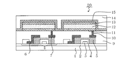
次に、本発明の有機発光素子を使用した表示装置について図1を用いて説明する。 Next, a display device using the organic light emitting device of the present invention will be described with reference to FIG.
図1は、本発明の有機発光素子と、この有機発光素子に電気接続するスイッチング素子の一例であるTFT素子と、を有する表示装置の例を示す断面模式図である。図1の表示装置20は、有機発光素子とTFT素子との組み合わせが2組図示されている。構造の詳細を以下に説明する。
FIG. 1 is a schematic cross-sectional view showing an example of a display device having the organic light-emitting element of the present invention and a TFT element which is an example of a switching element electrically connected to the organic light-emitting element. The
図1の表示装置20は、ガラス等の基板1とその上部にTFT素子又は有機化合物層を保護するための防湿膜2が設けられている。また符号3は金属のゲート電極3である。符号4はゲート絶縁膜4であり、5は半導体層である。
The
TFT素子8は半導体層5とドレイン電極6とソース電極7とを有している。TFT素子8の上部には絶縁膜9が設けられている。コンタクトホール10を介して有機発光素子の陽極11とソース電極7とが接続されている。表示装置はこの構成に限られず、陽極又は陰極のうちいずれか一方とTFT素子ソース電極又はドレイン電極のいずれか一方とが接続されていればよい。
The TFT element 8 has a semiconductor layer 5, a
尚、図1の表示装置20において、有機化合物層12は、単層あるいは多層の有機化合物層を1つの層の如く図示をしている。陰極13の上には有機発光素子の劣化を抑制するための第一の保護層14や第二の保護層15が設けられている。
In the
本発明の表示装置において、スイッチング素子に特に制限はなく、単結晶シリコン基板やMIM素子、a−Si型の素子等を用いてもよい。 In the display device of the present invention, the switching element is not particularly limited, and a single crystal silicon substrate, an MIM element, an a-Si type element, or the like may be used.
以下、実施例により本発明を説明する。ただし本発明はこれらに限定されるものではない。尚、後述する実施例のうち、実施例1乃至22は、本発明に該当する。 Hereinafter, the present invention will be described by way of examples. However, the present invention is not limited to these. Of the examples described later, Examples 1 to 22 correspond to the present invention.
[実施例1]例示化合物XX−1の合成 [Example 1] Synthesis of Exemplified Compound XX-1
(1)化合物X3の合成
以下に示す試薬、溶媒を反応容器内に投入した。
化合物X1:4.0g(13mmol)
化合物X2:2.8g(13mmol)
エタノール:65ml
(1) Synthesis of Compound X3 The following reagents and solvent were charged into the reaction vessel.
Compound X1: 4.0 g (13 mmol)
Compound X2: 2.8 g (13 mmol)
Ethanol: 65ml
次に、反応溶液を60℃まで加熱した後、6M水酸化ナトリウム水溶液10mlを滴下した。滴下終了後、反応溶液を80℃に加熱して、この温度(80℃)で2時間攪拌した。次に、反応溶液を冷却した後で生じる沈殿を濾取した。次に、得られた沈殿を、水、エタノールで順次洗浄した後、80℃で減圧加熱乾燥を行うことにより、濃緑色の固体である化合物X3を6g(収率:89%)得た。 Next, after heating the reaction solution to 60 ° C., 10 ml of 6M aqueous sodium hydroxide solution was added dropwise. After completion of the dropwise addition, the reaction solution was heated to 80 ° C. and stirred at this temperature (80 ° C.) for 2 hours. Next, the precipitate formed after the reaction solution was cooled was collected by filtration. Next, the obtained precipitate was washed successively with water and ethanol, and then dried under reduced pressure at 80 ° C. to obtain 6 g (yield: 89%) of Compound X3 as a dark green solid.
(2)化合物X5の合成
以下に示す試薬、溶媒を反応容器内に投入した。
化合物X3:5.0g(10mmol)
化合物X4:6.1g(21mmol)
キシレン:100ml
(2) Synthesis of Compound X5 The following reagents and solvent were charged into the reaction vessel.
Compound X3: 5.0 g (10 mmol)
Compound X4: 6.1 g (21 mmol)
Xylene: 100ml
次に、反応溶液を120℃まで加熱した後、亜硝酸イソアミル6g(21mmol)をゆっくり滴下した。次に、反応溶液を140℃に加熱して、この温度(140℃)で3時間攪拌した。次に、反応溶液を冷却した後、この反応溶液を減圧濃縮することで茶褐色の液体を得た。これをカラムクロマトグラフィー(展開溶媒;トルエン:ヘプタン=2:3)にて精製した後、クロロホルム/メタノールで再結晶を行うことにより、黄色結晶の化合物X5を4.6g(収率:65%)得た。 Next, after heating the reaction solution to 120 ° C., 6 g (21 mmol) of isoamyl nitrite was slowly added dropwise. Next, the reaction solution was heated to 140 ° C. and stirred at this temperature (140 ° C.) for 3 hours. Next, after cooling the reaction solution, the reaction solution was concentrated under reduced pressure to obtain a brown liquid. This was purified by column chromatography (developing solvent; toluene: heptane = 2: 3) and then recrystallized from chloroform / methanol to obtain 4.6 g of yellow crystal compound X5 (yield: 65%). Obtained.
(3)例示化合物XX−1の合成
以下に示す試薬、溶媒を反応容器内に投入した。
化合物X5:1.0g(1.5mmol)
化合物X6:0.55g(2.2mmol)
DMF:20ml
ビス(ジベンジリデンアセトン)パラジウム(0):0.84g(1.5mmol)
1,8―ジアザビシクロ[5.4.0]ウンデセ−7−エン:0.44g(2.9mmol)
トリシクロヘキシルフォスフィン:0.81g(2.9mmol)
(3) Synthesis of Exemplified Compound XX-1 The following reagents and solvent were charged into the reaction vessel.
Compound X5: 1.0 g (1.5 mmol)
Compound X6: 0.55 g (2.2 mmol)
DMF: 20ml
Bis (dibenzylideneacetone) palladium (0): 0.84 g (1.5 mmol)
1,8-diazabicyclo [5.4.0] undec-7-ene: 0.44 g (2.9 mmol)
Tricyclohexylphosphine: 0.81 g (2.9 mmol)
次に、反応溶液を150℃に加熱して、この温度(150℃)で4時間攪拌を行った。次に、反応溶液を冷却した後、この反応溶液を減圧濃縮することで赤黒色固体を得た。次に、得られた固体をカラムクロマトグラフィー(展開溶媒;トルエン:ヘプタン=1:3)にて精製した後、クロロホルム/メタノールで再結晶することにより、暗赤色の例示化合物XX−1を247mg(収率:26%)得た。 Next, the reaction solution was heated to 150 ° C. and stirred at this temperature (150 ° C.) for 4 hours. Next, after cooling the reaction solution, the reaction solution was concentrated under reduced pressure to obtain a red-black solid. Next, the obtained solid was purified by column chromatography (developing solvent; toluene: heptane = 1: 3), and then recrystallized from chloroform / methanol to obtain 247 mg (Example XX-1 of dark red exemplified compound XX-1). (Yield: 26%).
この化合物の純度を、HPLCを用いて評価したところ、純度99%以上であることを確認した。 When the purity of this compound was evaluated using HPLC, it was confirmed that the purity was 99% or more.
また例示化合物XX−1のトルエン溶液(1×10⁻⁵mol/L)における発光スペクトルを測定した。具体的には、日立製F−4500を用いて、350nmの励起波長におけるフォトルミネッセンスの測定を行った。その結果、550nmに最大強度を有する発光スペクトルを得た。 Moreover, the emission spectrum in the toluene solution (1 * 10 < -5 > mol / L) of exemplary compound XX-1 was measured. Specifically, photoluminescence at an excitation wavelength of 350 nm was measured using Hitachi F-4500. As a result, an emission spectrum having a maximum intensity at 550 nm was obtained.
また日本電子(JEOL)社製、JMS−T100TD(DART−TOF−MASS)を用いて分子量を測定することで同定した。 Moreover, it identified by measuring the molecular weight using JEOL (JEOL) company make and JMS-T100TD (DART-TOF-MASS).
DART−TOF−MASS:M+H=563.2 DART-TOF-MASS: M + H = 563.2
[実施例2]例示化合物XX−2の合成 [Example 2] Synthesis of Exemplified Compound XX-2
(1)化合物X8の合成
以下に示す試薬、溶媒を反応容器内に投入した。
化合物X7:10g(55mmol)
化合物X2:12g(55mmol)
エタノール:200ml
(1) Synthesis of Compound X8 The following reagents and solvent were charged into the reaction vessel.
Compound X7: 10 g (55 mmol)
Compound X2: 12 g (55 mmol)
Ethanol: 200ml
次に、反応溶液を60℃まで加熱した後、6M水酸化ナトリウム水溶液20mlを滴下した。滴下終了後、反応溶液を80℃に加熱して、この温度(80℃)で2時間攪拌した。次に、反応溶液を冷却した後で生じる沈殿を濾取した。次に、得られた沈殿を、水、エタノールで順次洗浄した後、80℃で減圧加熱乾燥を行うことにより、濃緑色の固体である化合物X8を18g(収率:92%)得た。 Next, after heating the reaction solution to 60 ° C., 20 ml of 6M aqueous sodium hydroxide solution was added dropwise. After completion of the dropwise addition, the reaction solution was heated to 80 ° C. and stirred at this temperature (80 ° C.) for 2 hours. Next, the precipitate formed after the reaction solution was cooled was collected by filtration. Next, the obtained precipitate was washed successively with water and ethanol, and then dried under reduced pressure at 80 ° C., thereby obtaining 18 g (yield: 92%) of Compound X8 as a dark green solid.
(2)化合物X9の合成
以下に示す試薬、溶媒を反応容器内に投入した。
化合物X8:10g(28mmol)
化合物X4:17g(56mmol)
キシレン:100ml
(2) Synthesis of Compound X9 The following reagents and solvent were charged into the reaction vessel.
Compound X8: 10 g (28 mmol)
Compound X4: 17 g (56 mmol)
Xylene: 100ml
次に、反応溶液を120℃まで加熱した後、亜硝酸イソアミル6.6g(56mmol)をゆっくり滴下した。次に、反応溶液を140℃に加熱して、この温度(140℃)で3時間攪拌した。次に、反応溶液を冷却した後、この反応溶液を減圧濃縮することで茶褐色の液体を得た。これをカラムクロマトグラフィー(展開溶媒;トルエン:ヘプタン=2:3)にて精製した後、クロロホルム/メタノールで再結晶を行うことにより、黄色結晶の化合物X9を9.6g(収率:61%)得た。 Next, after heating the reaction solution to 120 ° C., 6.6 g (56 mmol) of isoamyl nitrite was slowly added dropwise. Next, the reaction solution was heated to 140 ° C. and stirred at this temperature (140 ° C.) for 3 hours. Next, after cooling the reaction solution, the reaction solution was concentrated under reduced pressure to obtain a brown liquid. This was purified by column chromatography (developing solvent; toluene: heptane = 2: 3) and then recrystallized from chloroform / methanol to obtain 9.6 g of yellow crystal compound X9 (yield: 61%). Obtained.
(3)例示化合物XX−2の合成
以下に示す試薬、溶媒を反応容器内に投入した。
化合物X9:2.0g(3.6mmol)
化合物X10:2.0g(5.3mmol)
DMF:40ml
ビス(ジベンジリデンアセトン)パラジウム(0):2.0g(3.6mmol)
1,8―ジアザビシクロ[5.4.0]ウンデセ−7−エン:1.1g(7.1mmol)
トリシクロヘキシルフォスフィン:2.0g(7.1mmol)
(3) Synthesis of Exemplary Compound XX-2 Reagents and solvents shown below were charged into the reaction vessel.
Compound X9: 2.0 g (3.6 mmol)
Compound X10: 2.0 g (5.3 mmol)
DMF: 40ml
Bis (dibenzylideneacetone) palladium (0): 2.0 g (3.6 mmol)
1,8-diazabicyclo [5.4.0] undec-7-ene: 1.1 g (7.1 mmol)
Tricyclohexylphosphine: 2.0 g (7.1 mmol)
次に、反応溶液を150℃に加熱して、この温度(150℃)で4時間攪拌を行った。次に、反応溶液を冷却した後、この反応溶液を減圧濃縮することで赤黒色固体を得た。次に、得られた固体をカラムクロマトグラフィー(展開溶媒;トルエン:ヘプタン=1:3)にて精製した後、クロロホルム/メタノールで再結晶することにより、暗赤色の例示化合物XX−2を580mg(収率:25%)得た。 Next, the reaction solution was heated to 150 ° C. and stirred at this temperature (150 ° C.) for 4 hours. Next, after cooling the reaction solution, the reaction solution was concentrated under reduced pressure to obtain a red-black solid. Next, the obtained solid was purified by column chromatography (developing solvent; toluene: heptane = 1: 3), and then recrystallized from chloroform / methanol to obtain 580 mg of dark red exemplified compound XX-2 ( (Yield: 25%).
この化合物の純度を、HPLCを用いて測定したところ、純度99%以上であることを確認した。 When the purity of this compound was measured using HPLC, it was confirmed that the purity was 99% or more.
また実施例1と同様の方法により、例示化合物XX−2のトルエン溶液(濃度:1×10⁻⁵mol/L)における発光スペクトルを測定した。その結果、550nmに最大強度を有する発光スペクトルを得た。 Moreover, the emission spectrum in the toluene solution (concentration: 1 × 10 −5 mol / L) of exemplary compound XX-2 was measured by the same method as in Example 1. As a result, an emission spectrum having a maximum intensity at 550 nm was obtained.
また日本電子(JEOL)社製、JMS−T100TD(DART−TOF−MASS)を用いて分子量を測定することで同定した。
DART−TOF−MASS:M+H=563.2
Moreover, it identified by measuring the molecular weight using JEOL (JEOL) company make and JMS-T100TD (DART-TOF-MASS).
DART-TOF-MASS: M + H = 563.2
[実施例3]例示化合物XX−5の合成
実施例2(1)において、化合物X2に代えて下記に示される化合物X11を使用する以外は、実施例2と同様の方法で合成を行うことにより、例示化合物XX−5を得た。
[Example 3] Synthesis of Exemplified Compound XX-5 In Example 2 (1), except that Compound X11 shown below was used instead of Compound X2, the synthesis was performed in the same manner as in Example 2. Example compound XX-5 was obtained.
この化合物の純度を、HPLCを用いて測定したところ、純度99.5%以上であることを確認した。 When the purity of this compound was measured using HPLC, it was confirmed that the purity was 99.5% or more.
また実施例1と同様の方法により、例示化合物XX−5のトルエン溶液(濃度:1×10⁻⁵mol/L)における発光スペクトルを測定した。尚、本実施例においては、励起波長を500nmとした。その結果、550nmに最大強度を有する発光スペクトルを得た。 Moreover, the emission spectrum in the toluene solution (concentration: 1 × 10 −5 mol / L) of exemplary compound XX-5 was measured by the same method as in Example 1. In this example, the excitation wavelength was 500 nm. As a result, an emission spectrum having a maximum intensity at 550 nm was obtained.
また日本電子(JEOL)社製、JMS−T100TD(DART−TOF−MASS)を用いて分子量を測定することで同定した。
DART−TOF−MASS:M+H=805.3
Moreover, it identified by measuring the molecular weight using JEOL (JEOL) company make and JMS-T100TD (DART-TOF-MASS).
DART-TOF-MASS: M + H = 805.3
[実施例4]例示化合物XX−10の合成
実施例2(1)において、化合物X7に代えて下記に示される化合物X12を使用する以外は、実施例2と同様の方法で合成を行うことにより、例示化合物XX−10を得た。
[Example 4] Synthesis of Exemplified Compound XX-10 By synthesizing in the same manner as in Example 2 except that Compound X12 shown below is used instead of Compound X7 in Example 2 (1). Example compound XX-10 was obtained.
この化合物の純度を、HPLCを用いて測定したところ、純度99.5%以上であることを確認した。 When the purity of this compound was measured using HPLC, it was confirmed that the purity was 99.5% or more.
また実施例1と同様の方法により、例示化合物XX−10のトルエン溶液(濃度:1×10⁻⁵mol/L)における発光スペクトルを測定した。尚、本実施例においては、励起波長を500nmとした。その結果、550nmに最大強度を有する発光スペクトルを得た。 Moreover, the emission spectrum in the toluene solution (concentration: 1 × 10 −5 mol / L) of Exemplified Compound XX-10 was measured by the same method as in Example 1. In this example, the excitation wavelength was 500 nm. As a result, an emission spectrum having a maximum intensity at 550 nm was obtained.
また日本電子(JEOL)社製、JMS−T100TD(DART−TOF−MASS)を用いて分子量を測定することで同定した。
DART−TOF−MASS:M+H=805.3
Moreover, it identified by measuring the molecular weight using JEOL (JEOL) company make and JMS-T100TD (DART-TOF-MASS).
DART-TOF-MASS: M + H = 805.3
[実施例5]例示化合物XY−1の合成
実施例1(3)において、化合物X6の代わりに下記に示されるX13を使用する以外は、実施例1と同様の方法で合成を行うことにより、例示化合物XY−1を得た。
Example 5 Synthesis of Exemplified Compound XY-1 In Example 1 (3), synthesis was carried out in the same manner as in Example 1 except that X13 shown below was used instead of compound X6. Exemplary compound XY-1 was obtained.
この化合物の純度を、HPLCを用いて測定したところ、純度99.5%以上であることを確認した。 When the purity of this compound was measured using HPLC, it was confirmed that the purity was 99.5% or more.
また実施例1と同様の方法により、例示化合物XY−1のトルエン溶液(濃度:1×10⁻⁵mol/L)における発光スペクトルを測定した。尚、本実施例においては、励起波長を450nmとした。その結果、553nmに最大強度を有する発光スペクトルを得た。 Moreover, the emission spectrum in the toluene solution (concentration: 1 × 10 −5 mol / L) of the exemplary compound XY-1 was measured by the same method as in Example 1. In this example, the excitation wavelength was 450 nm. As a result, an emission spectrum having a maximum intensity at 553 nm was obtained.
また日本電子(JEOL)社製、JMS−T100TD(DART−TOF−MASS)を用いて分子量を測定することで同定した。
DART−TOF−MASS:M+H=765.3
Moreover, it identified by measuring the molecular weight using JEOL (JEOL) company make and JMS-T100TD (DART-TOF-MASS).
DART-TOF-MASS: M + H = 765.3
[実施例6]例示化合物XY−3の合成
実施例2(1)において、化合物X2の代わりに下記に示されるX14を使用する以外は、実施例2と同様の方法で合成を行うことにより、例示化合物XY−3を得た。
Example 6 Synthesis of Exemplified Compound XY-3 In Example 2 (1), synthesis was carried out in the same manner as in Example 2 except that X14 shown below was used instead of compound X2. Exemplary compound XY-3 was obtained.
この化合物の純度を、HPLCを用いて測定したところ、純度99.5%以上であることを確認した。 When the purity of this compound was measured using HPLC, it was confirmed that the purity was 99.5% or more.
また実施例1と同様の方法により、例示化合物XY−1のトルエン溶液(濃度:1×10⁻⁵mol/L)における発光スペクトルを測定した。尚、本実施例においては、励起波長を450nmとした。その結果、552nmに最大強度を有する発光スペクトルを得た。 Moreover, the emission spectrum in the toluene solution (concentration: 1 × 10 −5 mol / L) of the exemplary compound XY-1 was measured by the same method as in Example 1. In this example, the excitation wavelength was 450 nm. As a result, an emission spectrum having a maximum intensity at 552 nm was obtained.
また日本電子(JEOL)社製、JMS−T100TD(DART−TOF−MASS)を用いて分子量を測定することで同定した。
DART−TOF−MASS:M+H=877.5
Moreover, it identified by measuring the molecular weight using JEOL (JEOL) company make and JMS-T100TD (DART-TOF-MASS).
DART-TOF-MASS: M + H = 877.5
[実施例7]
本実施例では、基板上に、陽極、ホール注入層、ホール輸送層、発光層、ホール・エキシトンブロッキング層、電子輸送層、陰極が順次形成された有機発光素子を作製した。以下に、本実施例で使用した材料の一部を示す。
[Example 7]
In this example, an organic light emitting device in which an anode, a hole injection layer, a hole transport layer, a light emitting layer, a hole / exciton blocking layer, an electron transport layer, and a cathode were sequentially formed on a substrate was produced. Below, some of the materials used in this example are shown.
まずガラス基板上に、ITOを成膜し、所望のパターニング加工を施すことによりITO電極(陽極)を形成した。このときITO電極の膜厚を100nmとした。このようにITO電極が形成された基板をITO基板として、以下の工程で使用した。 First, an ITO film was formed on a glass substrate, and an ITO electrode (anode) was formed by performing a desired patterning process. At this time, the film thickness of the ITO electrode was 100 nm. The substrate on which the ITO electrode was thus formed was used as an ITO substrate in the following steps.
次に、1×10⁻⁵Paの真空チャンバー内における抵抗加熱による真空蒸着を行って、上記ITO基板上に、下記表4に示す有機化合物層及び電極層を連続成膜した。尚、このとき対向する電極(金属電極層、陰極)の電極面積が3mm2となるようにした。 Next, vacuum deposition was performed by resistance heating in a vacuum chamber of 1 × 10 −5 Pa, and an organic compound layer and an electrode layer shown in Table 4 below were continuously formed on the ITO substrate. At this time, the electrode area of the opposing electrodes (metal electrode layer, cathode) was set to 3 mm 2 .
尚、本実施例において、G−2及びG−3は、いずれも表3に示されるH1である。即ち、本実施例の有機発光素子において、発光層は、表3中のH1をホストとし、例示化合物XX−1をゲストとする2成分系の層とも解釈することができる。 In this example, G-2 and G-3 are all H1 shown in Table 3. That is, in the organic light-emitting device of this example, the light-emitting layer can be interpreted as a two-component layer in which H1 in Table 3 is a host and Exemplified Compound XX-1 is a guest.
得られた素子について、素子の特性を測定・評価した。具体的には、電流電圧特性をヒューレッドパッカード社製・微小電流計4140Bで測定し、発光輝度は、トプコン社製BM7で測定した。測定の結果を表5に示す。 About the obtained element, the characteristic of the element was measured and evaluated. Specifically, the current-voltage characteristic was measured with a micro ammeter 4140B manufactured by Hured Packard, and the light emission luminance was measured with a BM7 manufactured by Topcon. Table 5 shows the measurement results.
[実施例8乃至17]
実施例7において、G−2、G−3及びゲストを、表5に示される化合物に適宜変更する以外は、実施例7と同様の方法により有機発光素子を作製した。得られた素子について実施例7と同様に素子の特性を測定・評価した。測定の結果を表5に示す。尚、表5において、G−2として使用したH2、H7、H10、H15、H17、H19、H21及びH23、並びにG−3として使用したH2、H7、H10、H17、H19、H21、H23及びH24は、それぞれ表3に示されるホストである。
[Examples 8 to 17]
In Example 7, an organic light-emitting device was produced in the same manner as in Example 7 except that G-2, G-3, and the guest were appropriately changed to the compounds shown in Table 5. About the obtained element, the characteristic of the element was measured and evaluated in the same manner as in Example 7. Table 5 shows the measurement results. In Table 5, H2, H7, H10, H15, H17, H19, H21 and H23 used as G-2, and H2, H7, H10, H17, H19, H21, H23 and H24 used as G-3. Are the hosts shown in Table 3, respectively.
[実施例18]
本実施例では、基板上に、陽極、ホール注入層、ホール輸送層、発光層、電子輸送層、電子注入層、陰極が順次形成された有機発光素子を作製した。尚、本実施例で作製される有機発光素子は共振構造を有している。以下に、本実施例で使用した材料の一部を示す。
[Example 18]
In this example, an organic light emitting device was fabricated in which an anode, a hole injection layer, a hole transport layer, a light emitting layer, an electron transport layer, an electron injection layer, and a cathode were sequentially formed on a substrate. In addition, the organic light emitting device manufactured in this example has a resonance structure. Below, some of the materials used in this example are shown.
まずスパッタリング法により、ガラス基板(支持体)上に、アルミニウム合金(AlNd)を成膜し反射性陽極を形成した。このとき反射性陽極の膜厚を100nmとした。次に、スパッタリング法により、反射性陽極上にITOを成膜し透明性陽極を形成した。このとき透明性陽極の膜厚を80nmとした。次に、この陽極の周辺にアクリル製の素子分離膜を膜厚1.5μmで形成した後、所望のパターニング成形を行い、半径3mmの開口部を設けた。次に、陽極が形成されている基板を、アセトン、イソプロピルアルコール(IPA)で順次超音波洗浄した。次に、IPAで煮沸洗浄してから乾燥させた。次に、この基板表面に対してUV/オゾン洗浄を施した。 First, an aluminum alloy (AlNd) was formed on a glass substrate (support) by a sputtering method to form a reflective anode. At this time, the thickness of the reflective anode was set to 100 nm. Next, ITO was formed into a film on the reflective anode by a sputtering method to form a transparent anode. At this time, the film thickness of the transparent anode was 80 nm. Next, after forming an acrylic element isolation film with a film thickness of 1.5 μm around the anode, desired patterning was performed to provide an opening with a radius of 3 mm. Next, the substrate on which the anode was formed was sequentially ultrasonically washed with acetone and isopropyl alcohol (IPA). Next, it was dried by boiling with IPA and then dried. Next, this substrate surface was subjected to UV / ozone cleaning.
次に、1×10⁻⁵Paの真空チャンバー内における抵抗加熱による真空蒸着を行って、上記ITO基板上に、下記表6に示す有機化合物層を連続成膜した。 Next, vacuum deposition was performed by resistance heating in a vacuum chamber of 1 × 10 −5 Pa, and organic compound layers shown in Table 6 below were continuously formed on the ITO substrate.
尚、本実施例において、G−13及びG−14は、いずれも表3に示されるH10である。即ち、本実施例の有機発光素子において、発光層は、表3中のH10をホストとし、例示化合物XX−1をゲストとする2成分系の層とも解釈することができる。 In this example, G-13 and G-14 are both H10 shown in Table 3. That is, in the organic light-emitting device of this example, the light-emitting layer can be interpreted as a two-component layer in which H10 in Table 3 is the host and exemplary compound XX-1 is the guest.
次に、スパッタリング法により、電子注入層上に、IZOを成膜して陰極を形成した。このとき陰極の膜厚を30nmとした。最後に、窒素雰囲気下において封止を行った。
以上により、有機発光素子を作製した。
Next, a cathode was formed by depositing IZO on the electron injection layer by sputtering. At this time, the thickness of the cathode was set to 30 nm. Finally, sealing was performed in a nitrogen atmosphere.
Thus, an organic light emitting device was produced.
得られた素子について、素子の特性を測定・評価した。具体的には、電流電圧特性をヒューレッドパッカード社製・微小電流計4140Bで測定し、発光輝度は、トプコン社製BM7で測定した。測定の結果を表7に示す。 About the obtained element, the characteristic of the element was measured and evaluated. Specifically, the current-voltage characteristic was measured with a micro ammeter 4140B manufactured by Hured Packard, and the light emission luminance was measured with a BM7 manufactured by Topcon. Table 7 shows the measurement results.
[実施例19乃至20]
実施例18において、G−13、G−14及びゲストを、表7に示される化合物に適宜変更する以外は、実施例18と同様の方法により有機発光素子を作製した。得られた素子について実施例18と同様に素子の特性を測定・評価した。測定の結果を表7に示す。尚、表7において、G−13として使用したH6及びH16、並びにG−14として使用したH21及びH24は、それぞれ表3に示されるホストである。
[Examples 19 to 20]
In Example 18, an organic light-emitting device was produced in the same manner as in Example 18 except that G-13, G-14, and the guest were appropriately changed to the compounds shown in Table 7. The device characteristics of the obtained device were measured and evaluated in the same manner as in Example 18. Table 7 shows the measurement results. In Table 7, H6 and H16 used as G-13, and H21 and H24 used as G-14 are hosts shown in Table 3, respectively.
[実施例21]
本実施例では、基板上に、陽極、ホール輸送層、第1発光層、第2発光層、ホール・エキシトンブロッキング層、電子輸送層、陰極が順次形成された有機発光素子を作製した。尚、本実施例の有機発光素子は発光層が複数あるので、各発光層に含まれるゲストが個別あるいは同時に発光する態様である。以下に、本実施例で使用した材料の一部を示す。
[Example 21]
In this example, an organic light emitting device was fabricated in which an anode, a hole transport layer, a first light emitting layer, a second light emitting layer, a hole / exciton blocking layer, an electron transport layer, and a cathode were sequentially formed on a substrate. In addition, since the organic light emitting element of a present Example has multiple light emitting layers, it is the aspect which the guest contained in each light emitting layer light-emits separately or simultaneously. Below, some of the materials used in this example are shown.
まずガラス基板上に、ITOを成膜し、所望のパターニング加工を施すことによりITO電極を形成した。このときITO電極の膜厚を100nmとした。このようにITO電極が形成された基板をITO基板として、以下の工程で使用した。 First, ITO was formed on a glass substrate, and an ITO electrode was formed by performing a desired patterning process. At this time, the film thickness of the ITO electrode was 100 nm. The substrate on which the ITO electrode was thus formed was used as an ITO substrate in the following steps.
次に、1×10⁻⁵Paの真空チャンバー内における抵抗加熱による真空蒸着を行って、上記ITO基板上に、下記表8に示す有機化合物層及び電極層を連続成膜した。尚、このとき対向する電極(金属電極層、陰極)の電極面積が3mm2となるようにした。 Next, vacuum deposition was performed by resistance heating in a vacuum chamber of 1 × 10 −5 Pa, and an organic compound layer and an electrode layer shown in Table 8 below were continuously formed on the ITO substrate. At this time, the electrode area of the opposing electrodes (metal electrode layer, cathode) was set to 3 mm 2 .
尚、本実施例において、G−22、G−23及びG−24は、それぞれ表3に示されるH10、H23、H8である。 In this embodiment, G-22, G-23, and G-24 are H10, H23, and H8 shown in Table 3, respectively.
得られた素子について、素子の特性を測定・評価した。具体的には、電流電圧特性をヒューレッドパッカード社製・微小電流計4140Bで測定し、発光輝度は、トプコン社製BM7で測定した。測定の結果を表9に示す。 About the obtained element, the characteristic of the element was measured and evaluated. Specifically, the current-voltage characteristic was measured with a micro ammeter 4140B manufactured by Hured Packard, and the light emission luminance was measured with a BM7 manufactured by Topcon. Table 9 shows the measurement results.
[実施例22、23]
実施例21において、G−22、G−23、G−24及びゲストを、表9に示される化合物に適宜変更する以外は、実施例22と同様の方法により有機発光素子を作製した。得られた素子について実施例22と同様に素子の特性を測定・評価した。測定の結果を表9に示す。尚、表9において、G−22として使用したH18及びH23、G−23として使用したH18及びH23、並びにG−24として使用したH4及びH10は、それぞれ表3に示されるホストである。
[Examples 22 and 23]
In Example 21, an organic light emitting device was produced in the same manner as in Example 22 except that G-22, G-23, G-24 and the guest were appropriately changed to the compounds shown in Table 9. About the obtained element, the characteristic of the element was measured and evaluated in the same manner as in Example 22. Table 9 shows the measurement results. In Table 9, H18 and H23 used as G-22, H18 and H23 used as G-23, and H4 and H10 used as G-24 are hosts shown in Table 3, respectively.
以上説明したように、本発明に係る有機化合物は、高い量子収率と黄色に適した発光を有する化合物である。このため本発明に係る有機化合物を有機発光素子の構成材料として用いた場合、良好な発光特性を有する発光素子を得ることができる。 As described above, the organic compound according to the present invention is a compound having a high quantum yield and light emission suitable for yellow. For this reason, when the organic compound according to the present invention is used as a constituent material of an organic light-emitting device, a light-emitting device having good light-emitting characteristics can be obtained.
8:TFT素子、11:陽極、12:有機化合物層、13:陰極 8: TFT element, 11: anode, 12: organic compound layer, 13: cathode
Claims (12)
前記R 3 乃至R 8 及び前記R 11 乃至R 20 のいずれかが、炭素数1乃至4のアルキル基を有してもよいアリール基であることを特徴とする、請求項1に記載の有機化合物。 Any one of R 1 and R 10 or R 2 and R 9 is an aryl group, pyrimidyl group and pyrazyl group which may have an alkyl group having 1 to 4 carbon atoms, and the other is A hydrogen atom,
2. The organic compound according to claim 1, wherein any one of R 3 to R 8 and R 11 to R 20 is an aryl group which may have an alkyl group having 1 to 4 carbon atoms . .
3のいずれか一項に記載の有機化合物。 The organic compound according to any one of claims 1 to 3, which has two or more tertiary butyl groups in the molecular structure.
前記陽極と前記陰極との間に配置される有機化合物層と、を有する有機発光素子であって、
前記有機化合物層の少なくとも一層に、請求項1乃至4のいずれか一項に記載の有機化合物が含まれることを特徴とする、有機発光素子。 An anode and a cathode;
An organic light emitting device having an organic compound layer disposed between the anode and the cathode,
An organic light-emitting element, wherein the organic compound according to claim 1 is contained in at least one layer of the organic compound layer.
子。 The organic light emitting device according to claim 5, wherein the organic compound is contained in a light emitting layer.
前記複数の画素が、請求項5乃至7のいずれか一項に記載の有機発光素子と、前記有機発光素子に電気接続されるTFT素子と、をそれぞれ有することを特徴とする、表示装置。 A display device having a plurality of pixels,
The display device, wherein each of the plurality of pixels includes the organic light emitting element according to claim 5 and a TFT element electrically connected to the organic light emitting element.
前記表示部が複数の画素を有し、
前記複数の画素が、請求項5乃至7のいずれか一項に記載の有機発光素子と、前記有機発光素子に電気接続されるTFT素子と、をそれぞれ有することを特徴とする、画像入力装置。 An image input device having an input unit for inputting image information and a display unit for outputting an image,
The display unit includes a plurality of pixels;
The image input device, wherein each of the plurality of pixels includes the organic light emitting element according to claim 5 and a TFT element electrically connected to the organic light emitting element.
装置。 An illuminating device comprising the organic light-emitting element according to claim 5.
前記露光光源が、請求項5乃至7のいずれか一項に記載の有機発光素子を有することを特徴とする、画像形成装置。 An electrophotographic image forming apparatus having an exposure light source,
An image forming apparatus, wherein the exposure light source includes the organic light-emitting element according to claim 5.
前記露光光源は、請求項5乃至7のいずれか一項に記載の有機発光素子を有することを特徴とする、露光光源。The said exposure light source has an organic light emitting element as described in any one of Claims 5 thru | or 7, The exposure light source characterized by the above-mentioned.
Priority Applications (6)
| Application Number | Priority Date | Filing Date | Title |
|---|---|---|---|
| JP2011002263A JP5713686B2 (en) | 2011-01-07 | 2011-01-07 | Organic compound, organic light emitting device and image display device |
| EP11855218.1A EP2661418A4 (en) | 2011-01-07 | 2011-12-09 | Organic compound, organic light-emitting device, and image display device |
| US13/978,058 US9397298B2 (en) | 2011-01-07 | 2011-12-09 | Organic compound, organic light-emitting device, and image display device |
| CN201180063852XA CN103313957A (en) | 2011-01-07 | 2011-12-09 | Organic compound, organic light-emitting device, and image display device |
| PCT/JP2011/079261 WO2012093578A1 (en) | 2011-01-07 | 2011-12-09 | Organic compound, organic light-emitting device, and image display device |
| KR1020137020177A KR101555110B1 (en) | 2011-01-07 | 2011-12-09 | Organic compound, organic light-emitting device, and image display device |
Applications Claiming Priority (1)
| Application Number | Priority Date | Filing Date | Title |
|---|---|---|---|
| JP2011002263A JP5713686B2 (en) | 2011-01-07 | 2011-01-07 | Organic compound, organic light emitting device and image display device |
Publications (3)
| Publication Number | Publication Date |
|---|---|
| JP2012144459A JP2012144459A (en) | 2012-08-02 |
| JP2012144459A5 JP2012144459A5 (en) | 2014-02-20 |
| JP5713686B2 true JP5713686B2 (en) | 2015-05-07 |
Family
ID=46457438
Family Applications (1)
| Application Number | Title | Priority Date | Filing Date |
|---|---|---|---|
| JP2011002263A Active JP5713686B2 (en) | 2011-01-07 | 2011-01-07 | Organic compound, organic light emitting device and image display device |
Country Status (6)
| Country | Link |
|---|---|
| US (1) | US9397298B2 (en) |
| EP (1) | EP2661418A4 (en) |
| JP (1) | JP5713686B2 (en) |
| KR (1) | KR101555110B1 (en) |
| CN (1) | CN103313957A (en) |
| WO (1) | WO2012093578A1 (en) |
Families Citing this family (6)
| Publication number | Priority date | Publication date | Assignee | Title |
|---|---|---|---|---|
| JP6084001B2 (en) * | 2011-12-06 | 2017-02-22 | キヤノン株式会社 | Novel organic compound, organic light emitting device and image display device |
| JP5674707B2 (en) * | 2012-05-22 | 2015-02-25 | 株式会社東芝 | Display device |
| US9299959B2 (en) | 2012-06-06 | 2016-03-29 | Panasonic Intellectual Property Management Co., Ltd. | Inkjet device and manufacturing method for organic el device |
| US9266324B2 (en) | 2012-07-05 | 2016-02-23 | Panasonic Intellectual Property Management Co., Ltd. | Inkjet apparatus and method for manufacturing organic EL device |
| KR102284234B1 (en) * | 2012-07-23 | 2021-07-30 | 메르크 파텐트 게엠베하 | Derivatives of 2-diarylaminofluorene and organic electronic compounds containing them |
| EP3312159B1 (en) | 2015-06-16 | 2022-01-26 | Idemitsu Kosan Co., Ltd | Compound, material for organic electroluminescence element, organic electroluminescence element, and electronic device |
Family Cites Families (14)
| Publication number | Priority date | Publication date | Assignee | Title |
|---|---|---|---|---|
| JP3824417B2 (en) | 1997-04-04 | 2006-09-20 | 三井化学株式会社 | Hydrocarbon compounds and organic electroluminescent devices |
| JP3781517B2 (en) | 1997-07-22 | 2006-05-31 | 三井化学株式会社 | Organic electroluminescence device |
| US6866947B1 (en) * | 1999-12-28 | 2005-03-15 | Idemitsu Kosan Co., Ltd. | Organic electroluminescence device emitting white light |
| JP4255610B2 (en) * | 1999-12-28 | 2009-04-15 | 出光興産株式会社 | White organic electroluminescence device |
| JP4467170B2 (en) * | 2000-11-22 | 2010-05-26 | 三井化学株式会社 | Hydrocarbon compounds and organic electroluminescent devices |
| TWI314947B (en) * | 2002-04-24 | 2009-09-21 | Eastman Kodak Compan | Organic light emitting diode devices with improved operational stability |
| US6841267B2 (en) * | 2002-04-24 | 2005-01-11 | Eastman Kodak Company | Efficient electroluminescent device |
| US20040126617A1 (en) * | 2002-12-31 | 2004-07-01 | Eastman Kodak Company | Efficient electroluminescent device |
| JP4059822B2 (en) * | 2003-08-26 | 2008-03-12 | 三井化学株式会社 | Benzofluoranthene compound and organic electroluminescent device containing the benzofluoranthene compound |
| JP5080143B2 (en) * | 2007-06-19 | 2012-11-21 | 三井化学株式会社 | Aromatic hydrocarbon compound and organic electroluminescent device containing the aromatic hydrocarbon compound |
| US8129039B2 (en) * | 2007-10-26 | 2012-03-06 | Global Oled Technology, Llc | Phosphorescent OLED device with certain fluoranthene host |
| JP2009267135A (en) | 2008-04-25 | 2009-11-12 | Mitsui Chemicals Inc | Organic transistor |
| JP2009302470A (en) * | 2008-06-17 | 2009-12-24 | Mitsui Chemicals Inc | Organic transistor |
| JP5911377B2 (en) * | 2011-08-04 | 2016-04-27 | キヤノン株式会社 | Organic compound and organic light emitting device having the same |
-
2011
- 2011-01-07 JP JP2011002263A patent/JP5713686B2/en active Active
- 2011-12-09 US US13/978,058 patent/US9397298B2/en active Active
- 2011-12-09 CN CN201180063852XA patent/CN103313957A/en active Pending
- 2011-12-09 WO PCT/JP2011/079261 patent/WO2012093578A1/en active Application Filing
- 2011-12-09 EP EP11855218.1A patent/EP2661418A4/en not_active Withdrawn
- 2011-12-09 KR KR1020137020177A patent/KR101555110B1/en not_active IP Right Cessation
Also Published As
| Publication number | Publication date |
|---|---|
| EP2661418A1 (en) | 2013-11-13 |
| WO2012093578A1 (en) | 2012-07-12 |
| US20130292662A1 (en) | 2013-11-07 |
| JP2012144459A (en) | 2012-08-02 |
| EP2661418A4 (en) | 2016-02-24 |
| KR20130112933A (en) | 2013-10-14 |
| US9397298B2 (en) | 2016-07-19 |
| CN103313957A (en) | 2013-09-18 |
| KR101555110B1 (en) | 2015-09-22 |
Similar Documents
| Publication | Publication Date | Title |
|---|---|---|
| JP5791445B2 (en) | Novel organic compound, organic light emitting device and display device having the same | |
| EP2243761B1 (en) | Phenanthrene derivatives, light-emitting device and image display apparatus using the same | |
| KR101555111B1 (en) | Organic compound, organic electroluminescence element, and image display device | |
| JP5618647B2 (en) | Novel organic compound and organic light emitting device having the same | |
| JP5713686B2 (en) | Organic compound, organic light emitting device and image display device | |
| KR101490575B1 (en) | Novel organic compound and organic light-emitting device including the same | |
| WO2010071223A1 (en) | Novel organic compound | |
| JP4750893B1 (en) | Novel organic compounds and organic light emitting devices | |
| JP5627300B2 (en) | Novel organic compound and organic light emitting device having the same | |
| JP5578934B2 (en) | New organic compounds | |
| JP5704940B2 (en) | Organic compound, organic light emitting device and display device | |
| JP5586981B2 (en) | Novel organic compounds and organic light emitting devices | |
| JP5495665B2 (en) | Organic compound and organic light emitting device using the same | |
| JP2012188355A (en) | Novel organic compound, and organic light-emitting device | |
| JP2012148987A (en) | Organic compound, organic light-emitting element, and display device |
Legal Events
| Date | Code | Title | Description |
|---|---|---|---|
| A521 | Request for written amendment filed |
Free format text: JAPANESE INTERMEDIATE CODE: A523 Effective date: 20131226 |
|
| A621 | Written request for application examination |
Free format text: JAPANESE INTERMEDIATE CODE: A621 Effective date: 20131226 |
|
| A131 | Notification of reasons for refusal |
Free format text: JAPANESE INTERMEDIATE CODE: A131 Effective date: 20141111 |
|
| A521 | Request for written amendment filed |
Free format text: JAPANESE INTERMEDIATE CODE: A523 Effective date: 20150109 |
|
| TRDD | Decision of grant or rejection written | ||
| A01 | Written decision to grant a patent or to grant a registration (utility model) |
Free format text: JAPANESE INTERMEDIATE CODE: A01 Effective date: 20150210 |
|
| A61 | First payment of annual fees (during grant procedure) |
Free format text: JAPANESE INTERMEDIATE CODE: A61 Effective date: 20150310 |
|
| R151 | Written notification of patent or utility model registration |
Ref document number: 5713686 Country of ref document: JP Free format text: JAPANESE INTERMEDIATE CODE: R151 |