EP1355415B1 - Geschalteter Mikrofonpuffer - Google Patents
Geschalteter Mikrofonpuffer Download PDFInfo
- Publication number
- EP1355415B1 EP1355415B1 EP03252381A EP03252381A EP1355415B1 EP 1355415 B1 EP1355415 B1 EP 1355415B1 EP 03252381 A EP03252381 A EP 03252381A EP 03252381 A EP03252381 A EP 03252381A EP 1355415 B1 EP1355415 B1 EP 1355415B1
- Authority
- EP
- European Patent Office
- Prior art keywords
- switches
- switch
- buffer
- input
- state
- Prior art date
- Legal status (The legal status is an assumption and is not a legal conclusion. Google has not performed a legal analysis and makes no representation as to the accuracy of the status listed.)
- Expired - Lifetime
Links
- 239000000872 buffer Substances 0.000 title claims description 121
- 230000000295 complement effect Effects 0.000 claims description 22
- 238000000034 method Methods 0.000 claims description 10
- 239000003990 capacitor Substances 0.000 claims description 3
- 230000008859 change Effects 0.000 claims description 3
- 230000009977 dual effect Effects 0.000 description 5
- 238000012545 processing Methods 0.000 description 3
- 230000004044 response Effects 0.000 description 3
- 238000012986 modification Methods 0.000 description 2
- 230000004048 modification Effects 0.000 description 2
- 229910008062 Si-SiO2 Inorganic materials 0.000 description 1
- 229910006403 Si—SiO2 Inorganic materials 0.000 description 1
- 230000008901 benefit Effects 0.000 description 1
- 230000002596 correlated effect Effects 0.000 description 1
- 230000008878 coupling Effects 0.000 description 1
- 238000010168 coupling process Methods 0.000 description 1
- 238000005859 coupling reaction Methods 0.000 description 1
- 238000013461 design Methods 0.000 description 1
- 238000011161 development Methods 0.000 description 1
- 238000010586 diagram Methods 0.000 description 1
- 238000011160 research Methods 0.000 description 1
- 238000005070 sampling Methods 0.000 description 1
- 230000006641 stabilisation Effects 0.000 description 1
- 238000011105 stabilization Methods 0.000 description 1
Images


Classifications
-
- H—ELECTRICITY
- H03—ELECTRONIC CIRCUITRY
- H03F—AMPLIFIERS
- H03F1/00—Details of amplifiers with only discharge tubes, only semiconductor devices or only unspecified devices as amplifying elements
- H03F1/30—Modifications of amplifiers to reduce influence of variations of temperature or supply voltage or other physical parameters
- H03F1/303—Modifications of amplifiers to reduce influence of variations of temperature or supply voltage or other physical parameters using a switching device
-
- H—ELECTRICITY
- H03—ELECTRONIC CIRCUITRY
- H03F—AMPLIFIERS
- H03F1/00—Details of amplifiers with only discharge tubes, only semiconductor devices or only unspecified devices as amplifying elements
- H03F1/26—Modifications of amplifiers to reduce influence of noise generated by amplifying elements
-
- H—ELECTRICITY
- H03—ELECTRONIC CIRCUITRY
- H03F—AMPLIFIERS
- H03F3/00—Amplifiers with only discharge tubes or only semiconductor devices as amplifying elements
- H03F3/181—Low-frequency amplifiers, e.g. audio preamplifiers
- H03F3/183—Low-frequency amplifiers, e.g. audio preamplifiers with semiconductor devices only
- H03F3/185—Low-frequency amplifiers, e.g. audio preamplifiers with semiconductor devices only with field-effect devices
Definitions
- This invention relates to input buffer circuits for a microphone. More specifically, the present invention is directed to a method and apparatus for reducing and/or eliminating excess noise in an electret microphone buffer circuit.
- Assisted-listening systems and/or devices may utilize an electret microphone for converting sound energy to an electrical signal, signal processing circuitry for processing the electrical signal, and a receiver for converting the electrical signal to acoustical energy.
- the signal processing circuitry includes input buffer circuitry having an input impedance to match the output impedance of the electret microphone.
- the input buffer circuitry often includes a MOS transistor that is subject to undesirable 1/f noise, also called excess noise, or flicker noise.
- US-B1-6 353 344 describes an input buffer circuit for a hearing aid microphone.
- the present invention is directed to solve these and other problems.
- the invention consists in an input buffer circuit as defined in claim 1 and a method for substantially reducing and virtually eliminating direct current flow through the input transistor of an input buffer circuit for an electret microphone as defined in claim 12.
- a first switching control signal and a first set of switches cooperate to control the input transistor.
- the first set of switches comprises a first, second, and third switch. Each switch of the first set of switches has an "on” state and an “off” state. Each switch of the first set of switches is responsive to the first switching control signal.
- a second switching control signal and a second set of switches cooperate to control the input transistor.
- the second set of switches comprises a first, second, and third switch. Each switch of the second set of switches has an "on” state and an "off3 state responsive to the second switching signal.
- the first and second sets of switches compose a complementary set of switches wherein the "on" state of the first set of switches does not overlap with the "on" state of the second set of switches.
- the buffer circuit is a first resistor and a second resistor.
- the first resistor is operably connected to the input transistor, the first switch of the second set of switches, and the second and third switches of the first set of switches.
- the second resistor is operably connected to the input transistor, the first switch of the first set of switches, and the second and third switches of the second set of switches.
- An output of the input buffer circuit is operably connected to the input transistor and the third switch of both the first set and second set of switches.
- the output is operably responsive to the input transistor and the complementary set of switches wherein the mutually exclusive non-overlapping "on" states of the complementary set of switches alternately change the direction of current flow through the input transistor.
- the first and second buffer may compose a complementary set of buffers wherein the first and second buffers are controlled by their respective set of switches to ensure that either the first buffer or the second buffer is "on".
- the output of the input buffer circuit is operably connected to the first and second buffers wherein the mutually exclusive non-oveglapping "on" states of the complementary set of buffers substantially reduce the flow of direct current through the input transistors of the input buffer circuit.
- the 1/f noise of the input MOS transistor dominates the overall noise performance of the electronics. Typically this excess noise increases the total A-weight integrated noise of the buffer circuitry by 8 - 12 dB over that of the thermal noise contribution alone.
- Many methods have been devised to minimize the 1/f noise contribution in the overall system noise performance, such as correlated double sampling, chopper stabilization, etc., but none have addressed the fundamental source of the 1/f noise itself.
- the microphone buffer includes circuitry to substantially reduce the flow of direct current through the noise sensitive input transistor.
- a method for substantially reducing and virtually eliminating direct current flow through the input transistor of an input buffer circuit 10 for a microphone comprises providing an input transistor 12 operably connected to an input 14 and an output 16 of the input buffer circuit 10.
- the input transistor 12 has a first operating state having a direct current flow in a first direction and a second operating state having a direct current flow in a second direction.
- the direct current flow in the first direction is opposite to the direct current flow in the second direction.
- the input transistor 12 is biased to alternately operate between the first operating state and the second operating state wherein the opposing flow of direct current of the respective operating states cooperates to reduce the flow of direct current through the input buffer circuit 10.
- FIG. 1 A first embodiment of the present invention is shown in FIG. 1 .
- the input buffer circuit 10 for a microphone comprises the input 14 and the output 16.
- the input transistor 12 is operably connected to the input 14.
- a first set of switches comprises a first switch 18, a second switch 20, and a third switch 22. Each switch 18, 20, 22 of the first set of switches has an "on” state and an "off” state. Each switch 18, 20, 22 of the first set of switches is operably responsive to a first switching control signal.
- a second set of switches comprises a first switch 24, a second switch 26, and a third switch 28. Each switch 24, 26, 28 of the second set of switches has an "on” state and an "off” state. Each switch 24, 26, 28 of the second set of switches is operably responsive to a second switching control signal.
- a first resistor 30 and a second resistor 32 are operably connected to the input transistor 12.
- the first resistor 30 is connected to the first switch 24 of the second set of switches, and to the second switch 20 and third switch 22 of the first set of switches.
- the second resistor 32 is connected to the first switch 18 of the first set of switches, and to the second switch 26 and third switch 28 of the second set of switches.
- the output 16 of the input buffer circuit 10 is operably connected to the input transistor 12 and the third switches 22, 28 of the first set and second set of switches.
- the first 18, 20, 22 and second 24, 26, 28 sets of switches compose a complementary set of switches wherein the "on" state of the first set of switches does not overlap with the "on” state of the second set of switches.
- the complementary set of switches having non-overlapping "on” states alternately change the direction of the current flow through the buffer input transistor 12.
- the output 16 is operably responsive to the input transistor 12 and the complementary set of switches wherein the mutually exclusive non-overlapping "on" states of the complementary set of switches substantially reduce or virtually eliminate the DC current flow through the input transistor 12.
- the switches utilized in the first and second sets of switches are MOS transistors.
- the input transistor 12 is preferably a depletion NMOS type, DNMOS.
- the two switches 20, 26 that alternately connect the first 30 and second 32 resistors to ground will have a non-zero average, i.e., DC, current flow through them ⁇ the MOS transistors that form these switches 20, 26 ⁇ can be sufficiently large in area to essentially eliminate any significant 1/f noise that they may contribute.
- DC current flow to any subsequent circuitry connected to the output terminal 16 must be avoided.
- One technique that can be utilized to inhibit such DC current flow is to operably connect an AC coupling capacitor (not shown) to the output 16 of the input buffer circuit 10.
- an AC coupling capacitor not shown
- the two switches 24, 18, used to connect nodes V1 and V2 alternately to a battery terminal, VBAT do not contribute significant 1/f noise to the buffer despite the fact that a non-zero average current will flow, since these particular switches 24, 18 merely act as cascoding devices for the respective drain terminals of the input transistor 12. Cascoding devices are known to be well suited for low noise applications.
- An input buffer circuit 50 for a microphone (not shown) includes an input 52 and an output 54.
- a first buffer 56 is operably connected and responsive to a first complementary set of switches.
- a second buffer 58 is operably connected and responsive to a second complementary set of switches.
- the first and second buffers 56, 58 compose a complementary set of buffers wherein the first and second buffers are controlled by their respective set of switches to ensure that either the first buffer or the second buffer is operating in an "on" state.
- the output 54 is operably connected to the first buffer 56 and the second buffer 58 wherein the mutually exclusive non-overlapping "on" states of the complementary set of buffers reduce the flow of direct current through their input transistors 60, 80, respectively.
- the first buffer 56 of the input buffer circuit 50 of FIG. 2a comprises a first transistor 60 operably connected to the input 52 and the output 54.
- the first set of switches includes a first switch 62, a second switch 64, and a third switch 66. Each switch 62, 64, 66 of the first set of switches has an "on” state and an “off” state and is operably responsive to a first switching control signal 68, see FIG. 2b .
- the second set of switches of the first buffer 56 includes a first switch 72, a second switch 74, and a third switch 76.
- Each switch 72, 74, 76 of the second set of switches has an "on” state and an “off” state and is operably responsive to a second switching control signal 78, see FIG. 2b .
- the first 62, 64, 66 and second 72, 74, 76 sets of switches compose the first complementary set of switches wherein the "on" state of the first set of switches does not overlap with the "on” state of the second set of switches.
- a first resistor 70 is operably connected to the first transistor 60, the first switch 72 of the second set of switches, the second switch 64 of the first set of switches, and third switch 66 of the first set of switches.
- a second resistor 90 is operably connected to the first transistor 60, the first switch 62 of the first set of switches, the second switch 74 of the second set of switches, and the third 76 switch of the second set of switches.
- the second buffer 58 of the input buffer circuit 50 of FIG. 2a comprises a second transistor 80 operably connected to the input 52 and the output 54.
- a third set of switches includes a first 82 switch, a second switch 84, and a third switch 86.
- Each switch 82, 84, 86 of the third set of switches has an "on” state and an "off” state and is operably responsive to a third switching control signal 88, see FIG. 2b .
- a fourth set of switches of the second buffer 58 includes a first switch 92, a second switch 94, and a third switch 96.
- Each switch 92, 94, 96 of the fourth set of switches has an "on” state and an “off” state and is operably responsive to a fourth switching signal 98, see FIG. 2b .
- the third 82, 84, 86 and fourth 92, 94, 96 sets of switches compose a second complementary set of switches wherein the "on" state of the third set of switches does not overlap with the "on” state of the fourth set of switches.
- a third resistor 100 is operably connected to the second transistor 80, the first switch 92 of the fourth set of switches, the second switch 84 of the third set of switches, and third 86 switch of the third set of switches.
- a fourth resistor 102 is operably connected to the second transistor 80, the first switch 82 of the third set of switches, the second switch 94 of the fourth set of switches, and the third switch 96 of the fourth set of switches.
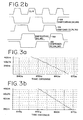
- the configuration shown in FIG. 2a along with the control signals in FIG. 2b , ensures that either the first buffer 56 or second buffer 58 is operating at all times.
- the input buffer circuit 10 of FIG. 1 is nearly identical to the first buffer 56 circuitry of FIG. 2a . Due to the non-overlapping first switch control signal 68 and second switch control signal 78, the input buffer circuit 10 of FIG. 1 and the first buffer 56 circuitry of FIG. 2a will experience a brief time duration wherein the buffer circuit is completely shut off. This shut off period results in an undesirable "flat" characteristic in the buffer circuit's output response, see FIG. 3a .
- the addition of the second buffer 58 configured in FIG. 2a improves the output response characteristic of FIG. 1 by ensuring that at least one of the two buffers 56, 58 is always on.
- the dual buffer circuit substantially reduces and eliminates the "flat" output region that occurs with the single input buffer circuit 10 of FIG. 1 , see FIG. 3b .
- the physical characteristics of the input transistors 56, 58 and resistors 70, 90, 100, 102 of the dual switched buffer circuit 50 should be modified. Because both the first buffer 56 and the second buffer of the dual buffer circuit 50 are "on" simultaneously most of the time, the sizes of the resistors 70, 90, 100, 102 and input transistors, 60, 80 should be modified. Preferably, the size of the two depletion NMOS transistors 60, 80 is approximately half the size of the single input transistor 12; and the value of the resistors 70, 90, 100, 102 are approximately twice the value of the resistors 30, 32 of the input buffer circuit 10 in FIG. 1 . These adjusted values for the dual buffer circuit 50 of FIG.
- FIG. 2b depicts the timing diagram of the switching control signals 68, 78, 88, 98 required to operate the first buffer 56 and the second buffer 58 of the buffer circuit 50 of FIG. 2a 90° out of phase with each other, in order to eliminate the "flat" output characteristic of the single buffer implementation.
Landscapes
- Engineering & Computer Science (AREA)
- Power Engineering (AREA)
- Multimedia (AREA)
- Amplifiers (AREA)
- Electronic Switches (AREA)
Claims (15)
- Eingangspuffer- Schaltung (10) für ein Mikrofon, umfassend einen Eingang (52); einen ersten Puffer (56) mit einem "Ein"- und einem "Aus"-Betriebszustand; einen zweiten Puffer (58) mit einem "Ein"- und einem "Aus"-Betriebszustand; eine Vorrichtung zur Steuerung des entsprechenden Betriebszustandes des ersten Puffers und des zweiten Puffers; und einem Ausgang (54), der mit dem ersten Puffer (56) und dem zweiten Puffer (58) betrieblich verbunden ist, wobei die Vorrichtung zur Steuerung mit dem ersten Puffer (56) und dem zweiten Puffer (58) zusammenarbeitet, um sicherzustellen, daß der eine oder der andere Puffer des ersten Puffers (56) und des zweiten Puffers (58) sich im "Ein"- Betriebszustand befindet und um den Fluß des direkten Stroms durch die Eingangstransistoren (60, 80) des ersten Puffers (56) bzw. des zweiten Puffers (58) erheblich zu reduzieren und virtuell zu eliminieren.
- Eingangspuffer- Schaltung nach Anspruch 1, dadurch gekennzeichnet, daß die Vorrichtung zur Steuerung ein erstes Schaltsignal und ein zweites Schaltsignal aufweist; daß ein erster Schaltersatz mit einem ersten, zweiten und dritten Schalter (62, 64, 66) vorhanden ist, wobei jeder Schalter des ersten Schaltersatzes (62, 64, 66) einen "Ein"- Zustand und einen "Aus"-Zustand hat und jeder Schalter des ersten Schaltersatzes (62, 64, 66) auf das erste Schaltsignal anspricht; sowie ein zweiter Schaltersatz mit einem ersten, zweiten und dritten Schalter (72, 74, 76); wobei jeder Schalter des zweiten Schaltersatzes (72, 74, 76) einen "Ein"- Zustand und einen "Aus"-Zustand hat und jeder Schalter des zweiten Schaltersatzes (72, 74, 76) auf das zweite Schaltsignal anspricht und die ersten und zweiten Schaltersätze (62, 64, 66, 72, 74, 76) einen komplementären Schaltersatz bilden, und der "Ein"- Zustand des ersten Schaltersatzes, der dem ersten Puffer des "Ein"-Betriebszustandes entspricht, nicht mit dem "Ein"- Zustand des zweiten Schaltersatzes überlappt, der dem zweiten Puffer des "Ein"-Betriebszustandes entspricht; ferner mit einem ersten Widerstand (70), der betrieblich mit dem Eingangstransistor (60), dem ersten Schalter (72) des zweiten Schaltersatzes sowie den zweiten und dritten Schaltern (64, 66) des ersten Schaltersatzes verbunden ist; und einem zweiten Widerstand (90), der betrieblich mit dem Eingangstransistor (60), dem ersten Schalter (62) des ersten Schaltersatzes und den zweiten und dritten Schaltern (74, 76) des zweiten Schaltersatzes verbunden ist; wobei darüber hinaus der Ausgang (54) mit dem Eingangstransistor (60) sowie dem dritten Schalter (66, 76) sowohl des ersten als auch des zweiten Schaltersatzes verbunden ist und der Ausgang (54) in Abhängigkeit von dem Eingangstransistor (60) und dem komplementären Schaltersatz (62, 64, 66, 72, 74, 76) betreibbar ist, und wobei die sich wechselweise exklusiv nicht überlappenden "Ein"- Zustände des komplementären Schaltersatzes (62, 64, 66, 72, 74, 76) alternativ die Stromrichtung des Flusses durch den Eingangstransistor (60) ändern.
- Eingangspuffer- Schaltung nach Anspruch 1, dadurch gekennzeichnet, daß die Vorrichtung zur Steuerung einen ersten Schaltersatz (62, 64, 66) aufweist; daß der erste Puffer (56) betrieblich auf den ersten Schaltersatz (62, 64, 66) anspricht; daß ein zweiter Schalterstz (72, 74, 76) vorhanden ist; daß ein zweiter Puffer (58) betrieblich auf den zweiten Schaltersatz (72, 74, 76) anspricht, daß der erste und der zweite Puffer (56, 58) einen komplementären Puffersatz bilden, in dem der erste und der zweite Puffer (56, 58) durch ihren entsprechenden Schaltersatz (62, 64, 66, 72, 74, 76) gesteuert werden, um sicherzustellen, daß entweder der erste Puffer (56) oder der zweite Puffer (58) "Ein"- geschaltet ist, und daß der Ausgang (54) betrieblich mit dem ersten und dem zweiten Puffer (56, 58) verbunden ist, wobei die wechselweise exklusiv nicht überlappenden "Ein"- Zustände des komplementären Puffersatzes den direkten Stromfluß durch die Eingangstransistoren (60, 80) in jedem ersten Puffer und zweiten Puffer (56, 58) erheblich verringern und virtuell eliminieren.
- Eingangspuffer- Schaltung nach Anspruch 3, dadurch gekennzeichnet, daß der erste Puffer (56) einen ersten Transistor (60) aufweist, der betrieblich mit dem Eingang (52) und dem Ausgang (54) verbunden ist; daß ein erstes Schaltsignal und ein erster Schaltersatz mit einem ersten, zweiten und dritten Schalter (62, 64, 66) vorhanden sind, wobei jeder Schalter (62, 64, 66) des ersten Schaltersatzes einen "Ein"- Zustand und einen "Aus"- Zustand hat und jeder Schalter (62, 64, 66) des ersten Schaltersatzes auf das erste Schaltsignal anspricht; daß ein zweiter Schaltersatz einen ersten, zweiten und dritten Schalter (72, 74, 76) aufweist, daß jeder Schalter (72, 74, 76) des zweiten Schaltersatzes einen "Ein"- Zustand und einen "Aus"- Zustand aufweist, und jeder Schalter (72, 74, 76) des zweiten Schaltersatzes auf das zweite Schaltsignal anspricht, daß die ersten und zweiten Schaltersätze (62, 64, 66, 72, 74, 76) einen ersten komplementären Schaltersatz bilden, bei dem der "Ein"- Zustand des ersten Schaltersatzes nicht mit dem "Ein"-Zustand des zweiten Schaltersatzes überlappt; daß ein erster Widerstand (70) mit dem ersten Transistor (60) betrieblich verbunden ist sowie dem ersten Schalter (72) des zweiten Schaltersatzes und dem zweiten und dem dritten Schalter (64, 66) des ersten Schaltersatzes, und daß ein zweiter Widerstand (90) mit dem ersten Transistor (60), dem ersten Schalter (62) des ersten Schaltersatzes und dem zweiten sowie dem dritten Schalter (74, 76) des zweiten Schaltersatzes betrieblich verbunden ist.
- Eingangspuffer- Schaltung nach Anspruch 3, dadurch gekennzeichnet, daß der zweite Puffer (58) einen zweiten Transistor (80) aufweist, der betrieblich mit dem Eingang (52), dem Ausgang (54) und dem ersten Transistor (60) verbunden ist, daß ein drittes Schaltsignal und ein viertes Schaltsignal vorhanden sind, die mit dem ersten bzw. dem zweiten Schaltsignal um 180 ° außer Phase sind; daß ein dritter Schaltersatz vorgesehen ist, der einen ersten, zweiten und dritten Schalter (82, 84, 86) aufweist, wobei jeder Schalter (82, 84, 86) des dritten Schaltersatzes einen "Ein"- Zustand und einen "Aus"- Zustand aufweist und jeder Schalter (82, 84, 86) des dritten Schaltersatzes auf das dritte Schaltsignal anspricht; daß ein vierter Schaltersatz vorhanden ist, der einen ersten, zweiten und dritten Schalter (92, 94, 96) aufweist, daß jeder Schalter (92, 94, 96) des vierten Schaltersatzes einen "Ein"- Zustand und einen "Aus"- Zustand hat und jeder Schalter (92, 94, 96) des vierten Schaltersatzes auf das vierte Schaltsignal anspricht, daß der dritte und vierte Schaltersatz (82, 84, 86, 92, 94, 96) einen zweiten komplementären Schaltersatz bilden, bei dem der "Ein"- Zustand des dritten Schaltersatzes nicht mit dem "Ein"- Zustand des vierten Schaltersatzes überlappt, daß ein dritter Widerstand (100) mit dem zweiten Transistor (90), dem ersten Schalter (92) des vierten Schaltersatzes und dem zweiten sowie dem dritten Schalter (84, 86) des dritten Schaltersatzes betrieblich verbunden ist, und daß ein vierter Widerstand (102) mit dem zweiten Transistor (90), dem ersten Schalter (82) des dritten Schaltersatzes und dem zweiten sowie dem dritten Schalter (94, 96) des vierten Schaltersatzes betrieblich verbunden ist, wobei entweder bei dem ersten oder dem zweiten Puffer sichergestellt ist, daß sie jederzeit arbeiten.
- Eingangspuffer- Schaltung nach einem der Ansprüche 1, 2 und 3, gekennzeichnet durch einen Kondensator, der mit dem Ausgang betrieblich gekoppelt ist, wobei der Gleichstrom daran gehindert wird, vor dem Ausgang wegzufließen.
- Eingangspuffer- Schaltung nach Anspruch 2 oder 3, dadurch gekennzeichnet, daß der erste Schaltersatz (62, 64, 66) einen MOS-Transistor aufweist.
- Eingangspuffer- Schaltung nach Anspruch 2 oder 3, dadurch gekennzeichnet, daß der zweite Schaltersatz (72, 74, 76) einen MOS-Transistor aufweist.
- Eingangspuffer- Schaltung nach einem der Ansprüche 1, 2 und 3, dadurch gekennzeichnet, daß der Transistor (60) einem DNMOS- Typ entspricht.
- Eingangspuffer- Schaltung nach Anspruch 5, dadurch gekennzeichnet, daß jeder der ersten, zweiten, dritten und vierten Schaltersätze (62, 64, 76, 72, 74, 76, 82, 84, 86, 92, 94, 96) einen MOS- Transistor aufweist.
- Eingangspuffer- Schaltung nach Anspruch 1, dadurch gekennzeichnet, daß jeder Puffer (56, 58) einen Eingangstransistor (60) aufweist.
- Verfahren zur erheblichen Verringerung und virtuellen Beseitigung des direkten Stromflusses durch den Eingangstransistor einer Eingangspuffer-Schaltung für ein dielektrisches Mikrofon, umfassend einen Eingangstransistor (60), der mit einem Eingang (52) und einem Ausgang (54) der Eingangspuffer- Schaltung (56, 58) betrieblich verbunden ist, wobei der Eingangstransistor (60) einen ersten Betriebszustand aufweist, in dem ein Stromfluß in einer ersten Richtung stattfindet, sowie einen zweiten Betriebszustand, in dem ein Stromfluß in einer zweiten Richtung stattfindet, wobei der Stromfluß in der ersten Richtung dem Stromfluß der zweiten Richtung entgegengesetzt ist, und wobei der Eingangstransistor (60) vorgespannt ist, um wechselnd zwischen dem ersten Betriebzustand und dem zweiten Betriebszustand zu arbeiten und wobei der entgegengesetzte Stromfluß der entsprechenden Betriebszustände dahingehend wirkt, daß der direkte Stromfluß durch den Eingangstransistor (60) der Pufferschaltung (56, 58) erheblich verringert und virtuell ausgeschaltet wird.
- Verfahren nach Anspruch 12, wobei das Vorspannen des Eingangstransistors (60) folgendes umfaßt: Schaffung eines Schalt-Steuersignals; Schaffung eines ersten Schaltersatzes mit einem ersten, zweiten und dritten Schalter (62, 64, 66), wobei jeder Schalter (2, 64, 66) des ersten Schaltersatzes einen "Ein"- Zustand und einen "Aus"- Zustand hat und jeder Schalter (62, 64, 66) des ersten Schaltersatzes auf das Schalt-Steuersignal anspricht; Schaffung eines zweiten Schaltersatzes mit einem ersten, zweiten und dritten Schalter (72, 74, 76), wobei jeder Schalter (72, 74, 76) des zweiten Schaltersatzes einen "Ein"- Zustand und einen "Aus"-Zustand hat, und jeder Schalter (72, 74, 76) des zweiten Schaltersatzes auf das Schalt- Steuersignal anspricht; Empfangen des Schalt- Steuersignals und Ändern des Betriebszustandes des ersten und zweiten Schaltersatzes (62, 64, 66, 72, 74, 76), wobei der "Ein"- Zustand des ersten Schaltersatzes (62, 64, 66) nicht den "Ein"- Zustand des zweiten Schaltersatzes (72, 74, 76) überlappt.
- Verfahren nach Anspruch 12, ferner umfassend die Beseitigung des Gleichstromflusses von der Ausgangsklemme (54) der Eingangspuffer-Schaltung.
- Verfahren nach Anspruch 14, dadurch gekennzeichnet, daß die Beseitigung des Gleichstromflusses von der Ausgangsklemme (54) der Eingangspuffer-Schaltung den Anschluß eines Kondensators in Reihe mit der Ausgangsklemme (54) der Eingangspuffer- Schaltung (56, 58) umfaßt.
Applications Claiming Priority (2)
| Application Number | Priority Date | Filing Date | Title |
|---|---|---|---|
| US37245102P | 2002-04-15 | 2002-04-15 | |
| US372451P | 2002-04-15 |
Publications (3)
| Publication Number | Publication Date |
|---|---|
| EP1355415A2 EP1355415A2 (de) | 2003-10-22 |
| EP1355415A3 EP1355415A3 (de) | 2004-05-06 |
| EP1355415B1 true EP1355415B1 (de) | 2009-10-21 |
Family
ID=28675595
Family Applications (1)
| Application Number | Title | Priority Date | Filing Date |
|---|---|---|---|
| EP03252381A Expired - Lifetime EP1355415B1 (de) | 2002-04-15 | 2003-04-15 | Geschalteter Mikrofonpuffer |
Country Status (4)
| Country | Link |
|---|---|
| US (1) | US7092538B2 (de) |
| EP (1) | EP1355415B1 (de) |
| DE (1) | DE60329731D1 (de) |
| DK (1) | DK1355415T3 (de) |
Families Citing this family (8)
| Publication number | Priority date | Publication date | Assignee | Title |
|---|---|---|---|---|
| US8139790B2 (en) * | 2008-05-15 | 2012-03-20 | Fortemedia, Inc. | Integrated circuit biasing a microphone |
| CN103563396B (zh) * | 2011-05-30 | 2016-12-28 | 索尼移动通信株式会社 | 用于减小对信号路径的干扰的方法、电路和设备 |
| US9590571B2 (en) | 2012-10-02 | 2017-03-07 | Knowles Electronics, Llc | Single stage buffer with filter |
| US9402131B2 (en) | 2013-10-30 | 2016-07-26 | Knowles Electronics, Llc | Push-pull microphone buffer |
| US9485594B2 (en) | 2014-08-06 | 2016-11-01 | Knowles Electronics, Llc | Connector arrangement in hearing instruments |
| US9859879B2 (en) | 2015-09-11 | 2018-01-02 | Knowles Electronics, Llc | Method and apparatus to clip incoming signals in opposing directions when in an off state |
| US11115744B2 (en) | 2018-04-02 | 2021-09-07 | Knowles Electronics, Llc | Audio device with conduit connector |
| US11536757B2 (en) | 2020-06-19 | 2022-12-27 | Knowles Electronics, Llc | Capacitive sensor assemblies and electrical circuits therefor |
Family Cites Families (9)
| Publication number | Priority date | Publication date | Assignee | Title |
|---|---|---|---|---|
| US3512100A (en) | 1968-07-03 | 1970-05-12 | Intern Research Products Inc | Audio frequency amplification circuit |
| US4063050A (en) | 1976-12-30 | 1977-12-13 | Industrial Research Products, Inc. | Acoustic transducer with improved electret assembly |
| US5083095A (en) | 1990-08-22 | 1992-01-21 | Knowles Electronics, Inc. | Plural source follower amplifier |
| US5097224A (en) | 1991-04-11 | 1992-03-17 | Telex Communications, Inc. | Self-biasing, low noise amplifier of extended dynamic range |
| US5589799A (en) | 1994-09-29 | 1996-12-31 | Tibbetts Industries, Inc. | Low noise amplifier for microphone |
| US6023194A (en) | 1997-05-23 | 2000-02-08 | Tibbetts Industries, Inc. | Amplifier with reduced input capacitance |
| NL1009544C2 (nl) | 1998-07-02 | 2000-01-10 | Microtronic Nederland Bv | Stelsel bestaande uit een microfoon en een voorversterker. |
| WO2000030249A1 (en) | 1998-11-12 | 2000-05-25 | Koninklijke Philips Electronics N.V. | Circuit comprising means for reducing the dc-offset and the noise produced by an amplifier |
| US6353344B1 (en) | 2000-05-22 | 2002-03-05 | Microtronic Us, Inc. | High impedance bias circuit |
-
2003
- 2003-04-11 US US10/412,460 patent/US7092538B2/en not_active Expired - Fee Related
- 2003-04-15 DE DE60329731T patent/DE60329731D1/de not_active Expired - Lifetime
- 2003-04-15 EP EP03252381A patent/EP1355415B1/de not_active Expired - Lifetime
- 2003-04-15 DK DK03252381.3T patent/DK1355415T3/da active
Also Published As
| Publication number | Publication date |
|---|---|
| US20030193354A1 (en) | 2003-10-16 |
| DK1355415T3 (da) | 2010-03-08 |
| EP1355415A2 (de) | 2003-10-22 |
| EP1355415A3 (de) | 2004-05-06 |
| DE60329731D1 (de) | 2009-12-03 |
| US7092538B2 (en) | 2006-08-15 |
Similar Documents
| Publication | Publication Date | Title |
|---|---|---|
| US5623550A (en) | Battery power supply circuit which supplies correct power polarity irrespective of battery orientation | |
| US20120007636A1 (en) | Analog switch for signal swinging between positive and negative voltages | |
| US8421518B2 (en) | High speed level shifters and method of operation | |
| EP1355415B1 (de) | Geschalteter Mikrofonpuffer | |
| TW200400688A (en) | Audio transient suppression circuits and methods | |
| TWI360295B (en) | Circuit for settling dc offset in direct conversio | |
| CN114374576A (zh) | 现场总线驱动电路 | |
| US8067986B2 (en) | Closed loop surge protection technique for differential amplifiers | |
| US8058926B2 (en) | Amplifier input switch configuration with improved PSRR | |
| US20030228024A1 (en) | Shock sound prevention circuit | |
| US6975100B2 (en) | Circuit arrangement for regulating the duty cycle of electrical signal | |
| US7760003B2 (en) | Controllable resistive circuit for providing a continuous variable resistance | |
| US7538604B2 (en) | Amplifier feedback switch configuration with improved PSRR | |
| US7368938B2 (en) | Input termination circuitry with high impedance at power off | |
| US20120068770A1 (en) | Anti-glitch system for audio amplifier | |
| TW200501560A (en) | BTL amplifier | |
| US6697612B2 (en) | Receiving section of a telephone | |
| US8410839B2 (en) | Systems and methods for driving high power states using lower voltage processes | |
| JPH0888551A (ja) | 電子スイッチ | |
| US20070109171A1 (en) | Audio ouput soft start by use of output driver enable signal | |
| EP1122923A2 (de) | Leitungstreiber mit Transformatorkopplung sowie Impedanzregelung | |
| US10965253B2 (en) | Mute mechanism with reduced pop noise in audio amplifier systems and methods | |
| CN217883391U (zh) | 高电压开关电路 | |
| JP3612510B2 (ja) | 前置増幅回路 | |
| US20250309786A1 (en) | Self-biasing inverter and control method thereof |
Legal Events
| Date | Code | Title | Description |
|---|---|---|---|
| PUAI | Public reference made under article 153(3) epc to a published international application that has entered the european phase |
Free format text: ORIGINAL CODE: 0009012 |
|
| AK | Designated contracting states |
Kind code of ref document: A2 Designated state(s): AT BE BG CH CY CZ DE DK EE ES FI FR GB GR HU IE IT LI LU MC NL PT RO SE SI SK TR |
|
| AX | Request for extension of the european patent |
Extension state: AL LT LV MK |
|
| PUAL | Search report despatched |
Free format text: ORIGINAL CODE: 0009013 |
|
| AK | Designated contracting states |
Kind code of ref document: A3 Designated state(s): AT BE BG CH CY CZ DE DK EE ES FI FR GB GR HU IE IT LI LU MC NL PT RO SE SI SK TR |
|
| AX | Request for extension of the european patent |
Extension state: AL LT LV MK |
|
| RIC1 | Information provided on ipc code assigned before grant |
Ipc: 7H 03F 3/45 B Ipc: 7H 03F 1/26 B Ipc: 7H 03F 3/185 B Ipc: 7H 03F 1/30 A |
|
| 17P | Request for examination filed |
Effective date: 20041103 |
|
| AKX | Designation fees paid |
Designated state(s): DE DK NL |
|
| 17Q | First examination report despatched |
Effective date: 20060918 |
|
| 17Q | First examination report despatched |
Effective date: 20060918 |
|
| GRAP | Despatch of communication of intention to grant a patent |
Free format text: ORIGINAL CODE: EPIDOSNIGR1 |
|
| GRAS | Grant fee paid |
Free format text: ORIGINAL CODE: EPIDOSNIGR3 |
|
| GRAA | (expected) grant |
Free format text: ORIGINAL CODE: 0009210 |
|
| AK | Designated contracting states |
Kind code of ref document: B1 Designated state(s): DE DK NL |
|
| REF | Corresponds to: |
Ref document number: 60329731 Country of ref document: DE Date of ref document: 20091203 Kind code of ref document: P |
|
| REG | Reference to a national code |
Ref country code: DK Ref legal event code: T3 |
|
| PLBE | No opposition filed within time limit |
Free format text: ORIGINAL CODE: 0009261 |
|
| STAA | Information on the status of an ep patent application or granted ep patent |
Free format text: STATUS: NO OPPOSITION FILED WITHIN TIME LIMIT |
|
| 26N | No opposition filed |
Effective date: 20100722 |
|
| PGFP | Annual fee paid to national office [announced via postgrant information from national office to epo] |
Ref country code: NL Payment date: 20101027 Year of fee payment: 8 Ref country code: DK Payment date: 20101029 Year of fee payment: 8 |
|
| PGFP | Annual fee paid to national office [announced via postgrant information from national office to epo] |
Ref country code: DE Payment date: 20101102 Year of fee payment: 8 |
|
| REG | Reference to a national code |
Ref country code: NL Ref legal event code: V1 Effective date: 20111101 |
|
| PG25 | Lapsed in a contracting state [announced via postgrant information from national office to epo] |
Ref country code: DE Free format text: LAPSE BECAUSE OF NON-PAYMENT OF DUE FEES Effective date: 20111101 Ref country code: NL Free format text: LAPSE BECAUSE OF NON-PAYMENT OF DUE FEES Effective date: 20111101 |
|
| REG | Reference to a national code |
Ref country code: DK Ref legal event code: EBP |
|
| REG | Reference to a national code |
Ref country code: DE Ref legal event code: R119 Ref document number: 60329731 Country of ref document: DE Effective date: 20111101 |
|
| PG25 | Lapsed in a contracting state [announced via postgrant information from national office to epo] |
Ref country code: DK Free format text: LAPSE BECAUSE OF NON-PAYMENT OF DUE FEES Effective date: 20110430 |