EP1353500B1 - Image sensor - Google Patents
Image sensor Download PDFInfo
- Publication number
- EP1353500B1 EP1353500B1 EP03075989A EP03075989A EP1353500B1 EP 1353500 B1 EP1353500 B1 EP 1353500B1 EP 03075989 A EP03075989 A EP 03075989A EP 03075989 A EP03075989 A EP 03075989A EP 1353500 B1 EP1353500 B1 EP 1353500B1
- Authority
- EP
- European Patent Office
- Prior art keywords
- transistor
- voltage
- reset
- drain
- source
- Prior art date
- Legal status (The legal status is an assumption and is not a legal conclusion. Google has not performed a legal analysis and makes no representation as to the accuracy of the status listed.)
- Expired - Lifetime
Links
Images


Classifications
-
- H—ELECTRICITY
- H04—ELECTRIC COMMUNICATION TECHNIQUE
- H04N—PICTORIAL COMMUNICATION, e.g. TELEVISION
- H04N25/00—Circuitry of solid-state image sensors [SSIS]; Control thereof
- H04N25/60—Noise processing, e.g. detecting, correcting, reducing or removing noise
- H04N25/65—Noise processing, e.g. detecting, correcting, reducing or removing noise applied to reset noise, e.g. KTC noise related to CMOS structures by techniques other than CDS
Definitions
- the invention relates to an image sensor and to an imager comprising an array of such sensors.
- Integrated circuits are being designed with lower supply voltages and that results in lower signal voltage swings and to maximise the signal voltage swing it is desirable to reduce the voltages dropped across the transistors.
- the invention provides an image sensor comprising a photosensitive element one side of which is connected to a first voltage; a reset transistor for resetting the potential at the other side of the photosensitive element to a given value; a source follower transistor whose gate is coupled to the other side of the photosensitive element, whose drain is connected to a second voltage, and whose source is connected via a load to the first voltage; and means for driving the reset transistor so that the given value is greater than the potential of the second voltage.
- the invention relates to an image sensor and to an imager comprising an array of such sensors.
- Integrated circuits are being designed with lower supply voltages and that results in lower signal voltage swings and to maximise the signal voltage swing it is desirable to reduce the voltages dropped across the transistors.
- EP-A-0905788 discloses a photoelectric conversion device having a plurality of pixel cells each of which includes a photoelectric conversion element, a field effect transistor having the gate area for storing signal charge generated by the photoelectric conversion element and the source-drain path for outputting a signal corresponding to the signal charge stored in the gate, a first power supply line for supplying electric power to the field effect transistor, and a first switch connected between the field effect transistor and the first power supply line, when a reset voltage for resetting the gate of the field effect transistor is V sig0 , a threshold voltage of the field effect transistor is V th , current flowing through the field effect transistor is I a , a voltage applied via the first power supply line is V cl , and a series resistance of the first switch is R on , each pixel is configured to satisfy a condition determined by V c ⁇ 1 - R on ⁇ I a > V sig ⁇ 0 - V th .
- EP-A-1117249 discloses an active pixel sensor soft reset circuit for reducing image lag while maintaining low reset kTC noise.
- the circuit pulls down the sensor potential to a sufficiently low level before the soft reset function is completed.
- the level to which the sensor potential is pulled is set between 0 and the critical potential at which the reset transistor will be on when the soft reset function begins.
- the timing of the pull down function is such that the sensor is stabilised at the low potential before the soft reset function completes.
- the sensor potential is pulled down using a pull-down circuit, which may consist of a CMOS type inverter.
- the sensor potential is pulled down by the bit line. Two ways in which the bit line may be pulled down are natural discharge, or by increasing the bias on the loading transistor. Two ways in which the bias on the loading transistor may be increased are a biasing circuit, or by using a pull-down transistor.
- the active pixel sensor may be implemented with any suitable sensor technology, such as photodiode, photogate, or pinned diode.
- the invention provides an image sensor comprising a photosensitive element one side of which is connected to a first voltage; a reset transistor for resetting the potential at the other side of the photosensitive element to a given value; a source follower transistor whose gate is coupled to the other side of the photosensitive element, whose drain is connected to a second voltage, and whose source is connected via a load to the first voltage; and means for driving the reset transistor so that the given value is greater than the potential of the second voltage plus the threshold voltage V th .of the source follower transistor.
- VTn or about 0.7 volts
- VDsatn or about 0.2 volts
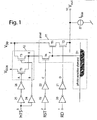
- an image sensor comprises a photosensitive element in the form of a photodiode D1 connected between a first voltage which in the implementation of Figure 1 is earthed and the gate electrode of an n channel field effect transistor T1 connected as a source follower.
- the source electrode of transistor T1 is connected via the source drain path of an n channel field effect transistor T2 whose drain electrode is connected to an output terminal 10.
- the drain electrode of transistor T1 is connected to a second voltage V DD .
- the source electrode of a p channel field effect transistor T3 is connected to the supply voltage V DD while its drain electrode is connected via the drain source path of an n channel field effect transistor T4 whose drain electrode is connected to the gate electrode of transistor T1.
- a second p channel field effect transistor T5 has its source electrode connected to a third supply voltage V DDR and its drain electrode connected to the drain electrode of transistor T3.
- Transistors T1, T2, T4 and diode D1 form a pixel element 11 while transistors T3 and T5 form a reset circuit 12.
- An input terminal 1 receives a row select signal which is fed via two inverters 20 and 21 to the gate electrode of transistor T2.
- a further input terminal 2 receives a pixel reset signal which is fed via two inverters 22 and 23 to the gate electrode of transistor T4.
- a further terminal 3 receives a hard reset signal which is fed via an inverter 24 to the gate electrode of transistor T3 and via two inverters 25 and 26 to the gate electrode of transistor T5.
- a current source 27 is connected between the first voltage and the terminal 10.
- the image sensor shown in Figure 1 is designed to form part of an image sensor array such as that shown in Figure 5 which operates in a column parallel (row-wise) fashion. Following the exposure of the pixel for an integration time T3 as shown in Figure 3 it is selected by pulsing RD high in Figure 3, RD being the potential applied to terminal 1. This causes the potential at the sense node F in Figure 1 and which reflects the photoelectrons accumulated during the integration time to be passed to the terminal 10 via the source follower transistor T1 and the pixel select transistor T2. The readout of the pixel takes place during time period T4 as shown in Figure 3.
- a reset procedure is carried out on the pixel to reset the photosensitive element to a given state. This is effected using the reset circuit 12 via the transistor T4.
- the reset signal RST applied to terminal 2 is high during time periods T1 and T2 as shown in Figure 3.
- the signal HST applied to terminal 3 is high during time period T1 and low at all other times. Consequently, the transistor T5 is switched on at all times apart from when the input HTS is high. Conversely, the transistor T3 is switched off when the signal HTS is low and is switched on when the signal HTS is high.
- a soft reset is produced as the drain of the reset transistor T4 is connected to a reset voltage VDDR having a value of 2.5 volts. Since this reset voltage is the same as that of the gate of the reset transistor T4 a soft reset is performed.
- the photodiode D1 is charged at a voltage higher than the drain voltage of the source follower transistor T1.
- the difference is about 0.4 to 0.5 volts higher than the supply voltage V DD .
- This overdrive of the source follower transistor T4 enables an improved signal voltage swing at the output of the pixel 10.
- the photodiode would be reset to a voltage equal to V DD . Consequently, the maximum voltage at node Vout is V DD - VTn where VTn is the threshold voltage of the source follower transistor T1.
- the minimum voltage at node Vout is given by the saturation voltage VDsatn of the current source 25.
- V DD 1.2 volts
- VDsatn 0.2 volts
- VTn 0.7 volts
- Figure 2 shows a second embodiment of an image sensor according to the invention. It is similar to the embodiment of Figure 1, the difference being that instead of the photosensitive element being a photodiode it is a photogate.
- the photogate PG is connected via a transfer gate TG to the node F which is a floating diffusion that is connected to the gate of transistor T1.
- the embodiment of Figure 2 is identical to that of Figure 1 and consequently no further description of the embodiment of Figure 2 will be given.
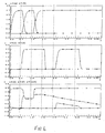
- Figure 4 shows the voltage waveforms at the nodes A, B, C, D, E, F and the Vout, that is terminal 10. It should be noted that the voltages quoted are typical voltages used presently in large scale integrated circuits using CMOS technology. They are not to be taken as limiting in any form the scope of the present invention. The actual voltages used will depend on the state of CMOS technology at the time of manufacture.
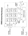
- FIG. 5 shows how the pixel sensor shown in Figures 1 and 2 can be integrated into an array of pixel sensors.
- each pixel element in the array includes a buffer circuit for reading out the pixel charges into a column buffer and from there into an output buffer 501.
- a row decoder 502 and column decoder 503 are provided.
- the row decoder 502 will provide the signal RD applied to input 1 of the pixel element to cause the accumulated charge to be read out onto the column busses to enable each pixel to read into its associated column buffer.
- the column decoder 503 produces signals causing the respective column buffer to read into the output buffer 501 to enable the pixel charges to be read out serially from the sensor.
- a basic three transistor scheme is used for each pixel.
- Any suitable photosensitive element can be used as the sensor.
- the two examples of a photodiode and a photogate are merely examples and not limitative.
- the concept of overdriving the source follower transistor T1 and the reset scheme using a voltage higher than that of the supply voltage to the pixel enables a larger output voltage swing to be obtained from each pixel sensor.
Landscapes
- Engineering & Computer Science (AREA)
- Multimedia (AREA)
- Signal Processing (AREA)
- Transforming Light Signals Into Electric Signals (AREA)
- Solid State Image Pick-Up Elements (AREA)
- Investigating Or Analyzing Materials By The Use Of Electric Means (AREA)
- Photoreceptors In Electrophotography (AREA)
- Glass Compositions (AREA)
Abstract
Description
- The invention relates to an image sensor and to an imager comprising an array of such sensors.
- Integrated circuits are being designed with lower supply voltages and that results in lower signal voltage swings and to maximise the signal voltage swing it is desirable to reduce the voltages dropped across the transistors.
- A prior art image sensor is described in a paper entitled "A Single-chip Programmable Digital CMOS Imager with Enhanced Low-light Detection Capability" by Bedabrata Pain, Guang Yuang, Monica Ortiz, Kenneth McCarty, Bruce Hancock, Julie Heynssens, Thomas Cunningham, Chris Wrigley and Charlie Ho, 13th International Conference on VLSI Design, Calcutta, India, January 4-7, 2000.
- The invention provides an image sensor comprising a photosensitive element one side of which is connected to a first voltage; a reset transistor for resetting the potential at the other side of the photosensitive element to a given value; a source follower transistor whose gate is coupled to the other side of the photosensitive element, whose drain is connected to a second voltage, and whose source is connected via a load to the first voltage; and means for driving the reset transistor so that the given value is greater than the potential of the second voltage.
- By resetting the photosensitive element to a voltage greater than the second voltage the voltage drop across the source follower can be reduced from VTn (or about 0.7 volts) to VDsatn (or about 0.2 volts). It should be noted that these are typical figures and that VTn is
- The invention relates to an image sensor and to an imager comprising an array of such sensors.
- Integrated circuits are being designed with lower supply voltages and that results in lower signal voltage swings and to maximise the signal voltage swing it is desirable to reduce the voltages dropped across the transistors.
- A prior art image sensor is described in a paper entitled "A Single-chip Programmable Digital CMOS Imager with Enhanced Low-light Detection Capability" by Bedabrata Pain, Guang Yuang, Monica Ortiz, Kenneth McCarty, Bruce Hancock, Julie Heynssens, Thomas Cunningham, Chris Wrigley and Charlie Ho, 13th International Conference on VLSI Design, Calcutta, India, January 4-7, 2000.
-
EP-A-0905788 discloses a photoelectric conversion device having a plurality of pixel cells each of which includes a photoelectric conversion element, a field effect transistor having the gate area for storing signal charge generated by the photoelectric conversion element and the source-drain path for outputting a signal corresponding to the signal charge stored in the gate, a first power supply line for supplying electric power to the field effect transistor, and a first switch connected between the field effect transistor and the first power supply line, when a reset voltage for resetting the gate of the field effect transistor is Vsig0, a threshold voltage of the field effect transistor is Vth, current flowing through the field effect transistor is Ia, a voltage applied via the first power supply line is Vcl, and a series resistance of the first switch is Ron, each pixel is configured to satisfy a condition determined by
-
EP-A-1117249 discloses an active pixel sensor soft reset circuit for reducing image lag while maintaining low reset kTC noise. The circuit pulls down the sensor potential to a sufficiently low level before the soft reset function is completed. The level to which the sensor potential is pulled is set between 0 and the critical potential at which the reset transistor will be on when the soft reset function begins. The timing of the pull down function is such that the sensor is stabilised at the low potential before the soft reset function completes. In one embodiment, the sensor potential is pulled down using a pull-down circuit, which may consist of a CMOS type inverter. In another embodiment, the sensor potential is pulled down by the bit line. Two ways in which the bit line may be pulled down are natural discharge, or by increasing the bias on the loading transistor. Two ways in which the bias on the loading transistor may be increased are a biasing circuit, or by using a pull-down transistor. The active pixel sensor may be implemented with any suitable sensor technology, such as photodiode, photogate, or pinned diode. - The invention provides an image sensor comprising a photosensitive element one side of which is connected to a first voltage; a reset transistor for resetting the potential at the other side of the photosensitive element to a given value; a source follower transistor whose gate is coupled to the other side of the photosensitive element, whose drain is connected to a second voltage, and whose source is connected via a load to the first voltage; and means for driving the reset transistor so that the given value is greater than the potential of the second voltage plus the threshold voltage Vth.of the source follower transistor.
- By resetting the photosensitive element to a voltage greater than the second voltage the voltage drop across the source follower can be reduced from VTn (or about 0.7 volts) to VDsatn (or about 0.2 volts). It should be noted that these are typical figures and that VTn is process dependent whereas VDsatn is design dependent. When the supply voltage is 1.2 volts this is a significant reduction.
- Further additional, optional, or advantageous features are disclosed in the claims appended hereto to which reference should now be made.
- The above and other features and advantages of the invention will be apparent from the following description, by way of example, of an embodiment of the invention with reference to the accompanying drawings, in which;-
- Figure 1 is a circuit diagram of a first embodiment of an image sensor according to the invention,
- Figure 2 is a circuit diagram of a second embodiment of an image sensor according to the invention,
- Figure 3 shows control waveforms applied to the image sensor,
- Figure 4 shows waveforms at selected points within the sensor of Figure 2, and
- Figure 5 shows an array of image sensors.
- As shown in Figure 1 an image sensor comprises a photosensitive element in the form of a photodiode D1 connected between a first voltage which in the implementation of Figure 1 is earthed and the gate electrode of an n channel field effect transistor T1 connected as a source follower. The source electrode of transistor T1 is connected via the source drain path of an n channel field effect transistor T2 whose drain electrode is connected to an
output terminal 10. The drain electrode of transistor T1 is connected to a second voltage VDD. The source electrode of a p channel field effect transistor T3 is connected to the supply voltage VDD while its drain electrode is connected via the drain source path of an n channel field effect transistor T4 whose drain electrode is connected to the gate electrode of transistor T1. A second p channel field effect transistor T5 has its source electrode connected to a third supply voltage VDDR and its drain electrode connected to the drain electrode of transistor T3. Transistors T1, T2, T4 and diode D1 form apixel element 11 while transistors T3 and T5 form areset circuit 12. - An
input terminal 1 receives a row select signal which is fed via twoinverters further input terminal 2 receives a pixel reset signal which is fed via twoinverters further terminal 3 receives a hard reset signal which is fed via aninverter 24 to the gate electrode of transistor T3 and via twoinverters current source 27 is connected between the first voltage and theterminal 10. - The image sensor shown in Figure 1 is designed to form part of an image sensor array such as that shown in Figure 5 which operates in a column parallel (row-wise) fashion. Following the exposure of the pixel for an integration time T3 as shown in Figure 3 it is selected by pulsing RD high in Figure 3, RD being the potential applied to
terminal 1. This causes the potential at the sense node F in Figure 1 and which reflects the photoelectrons accumulated during the integration time to be passed to theterminal 10 via the source follower transistor T1 and the pixel select transistor T2. The readout of the pixel takes place during time period T4 as shown in Figure 3. - Prior to the integration time T3 a reset procedure is carried out on the pixel to reset the photosensitive element to a given state. This is effected using the
reset circuit 12 via the transistor T4. The reset signal RST applied toterminal 2 is high during time periods T1 and T2 as shown in Figure 3. The signal HST applied toterminal 3 is high during time period T1 and low at all other times. Consequently, the transistor T5 is switched on at all times apart from when the input HTS is high. Conversely, the transistor T3 is switched off when the signal HTS is low and is switched on when the signal HTS is high. This can be seen from waveform V(E) in Figure 4 where it can be seen that the drain of transistor T4 is connected to the potential VDDR when the signal HTS is low and to the supply VDD via transistor T3 when HTS is high. Thus during the first phase in time period T1 the drain of the transistor T4 is connected to the supply voltage VDD which may, for example be 1.2 volts, through the p channel transistor T3. Consequently, since the gate voltage of transistor T4 is 2.5 volts the photodiode is fully reset to 1.2 volts through a hard reset operation. During the second phase, that is time T2 when the signal HTS is low, a soft reset is produced as the drain of the reset transistor T4 is connected to a reset voltage VDDR having a value of 2.5 volts. Since this reset voltage is the same as that of the gate of the reset transistor T4 a soft reset is performed. - In the paper by Pain et al a soft reset scheme is described but there is only one supply voltage line for the pixel, the reset and source follower transistors have the same drain connection. The reset gate voltage is not higher than the pixel supply voltage. In the first phase where the signal HTS is high the pixel supply voltage is connected to VDD through an NMOS transistor with its gate connected to VDD. Consequently, the pixel supply voltage is reduced by VTn and since the gate voltage of the reset transistor is VDD a hard reset is performed. In the second phase where the signal HTS is low the pixel supply voltage is connected to VDD through a PMOS transistor whose gate is connected to VSS. Therefore the pixel supply voltage is equal to VDD and also equal to the reset transistor gate voltage.
- In the pixel shown in Figure 1 the photodiode D1 is charged at a voltage higher than the drain voltage of the source follower transistor T1. The difference is about 0.4 to 0.5 volts higher than the supply voltage VDD. This overdrive of the source follower transistor T4 enables an improved signal voltage swing at the output of the
pixel 10. In the embodiment shown by Pain et al the photodiode would be reset to a voltage equal to VDD. Consequently, the maximum voltage at node Vout is VDD - VTn where VTn is the threshold voltage of the source follower transistor T1. The minimum voltage at node Vout is given by the saturation voltage VDsatn of thecurrent source 25. This gives a maximum voltage atterminal 10 of VDD - VTn and a minimum voltage atoutput 10 of VSS + VDsatn. If VDD equals 1.2 volts, VDsatn equals 0.2 volts, and VTn equals 0.7 volts, then the maximum voltage swing atoutput 10 is equal to 0.4 volts. - Conversely, if the photodiode D1 is reset to a supply voltage higher than VDD the VTn voltage drop can be eliminated. This gives a maximum voltage at
output 10 of VDD - VDsatn and a minimum voltage ofoutput 10 at VSS + VDsatn. Using the same values for VDD and VDsatn, this gives a maximum voltage swing atterminal 10 of 0.8 volts. Thus by charging the photodiode to a voltage higher than the drain voltage of the source follower the maximum output voltage swing is significantly increased. - Figure 2 shows a second embodiment of an image sensor according to the invention. It is similar to the embodiment of Figure 1, the difference being that instead of the photosensitive element being a photodiode it is a photogate. The photogate PG is connected via a transfer gate TG to the node F which is a floating diffusion that is connected to the gate of transistor T1. In other respects the embodiment of Figure 2 is identical to that of Figure 1 and consequently no further description of the embodiment of Figure 2 will be given.
- Figure 4 shows the voltage waveforms at the nodes A, B, C, D, E, F and the Vout, that is terminal 10. It should be noted that the voltages quoted are typical voltages used presently in large scale integrated circuits using CMOS technology. They are not to be taken as limiting in any form the scope of the present invention. The actual voltages used will depend on the state of CMOS technology at the time of manufacture.
- Figure 5 shows how the pixel sensor shown in Figures 1 and 2 can be integrated into an array of pixel sensors. As shown in Figure 5, each pixel element in the array includes a buffer circuit for reading out the pixel charges into a column buffer and from there into an
output buffer 501. Arow decoder 502 andcolumn decoder 503 are provided. Therow decoder 502 will provide the signal RD applied to input 1 of the pixel element to cause the accumulated charge to be read out onto the column busses to enable each pixel to read into its associated column buffer. Thecolumn decoder 503 produces signals causing the respective column buffer to read into theoutput buffer 501 to enable the pixel charges to be read out serially from the sensor. - As can be seen from the foregoing description, a basic three transistor scheme is used for each pixel. Any suitable photosensitive element can be used as the sensor. The two examples of a photodiode and a photogate are merely examples and not limitative. The concept of overdriving the source follower transistor T1 and the reset scheme using a voltage higher than that of the supply voltage to the pixel enables a larger output voltage swing to be obtained from each pixel sensor.
Claims (5)
- An image sensor for use in a pixel array comprising a photosensitive element (D1) one side of which is connected to a first voltage; a reset transistor (T4) for resetting the potential at the other side of the photosensitive element (D1) to a given value; a source follower transistor (T1) whose gate is coupled to the other side of the photosensitive element (D1), whose drain is connected to a second voltage (VDD), and whose source is connected via a load (27) to the first voltage; a select transistor (T2) having its drain source path connected between the source of the source follower (T1) and the load (27) and its gate connected to a select input (1); and means for driving the reset transistor (T4) so that the given value is greater than the potential of the second voltage (VDD).
- A sensor as claimed in Claim 1 in which the reset transistor (T4) is connected as a source follower and the means for driving the reset transistor (T4) comprises means for applying a potential greater than that of the second voltage to the gate and drain of the reset transistor.
- A sensor as claimed in Claim 2 in which the reset (T4) and source follower (T1) transistors are n channel field effect transistors and the means for driving the reset transistor (T4) comprises a first p channel field effect transistor (T3) whose drain is connected to the drain of the reset transistor (T4) and whose source is connected to the second voltage (VDD), a second p channel field effect transistor (T5) whose drain is connected to the reset transistor (T4) and whose source is connected to a potential (VDDR) greater than that of the second voltage (VDD), means (2) for applying a reset pulse whose amplitude is greater than that of the second voltage (VDD) to the gate of the reset transistor (T4), means for causing the first p channel transistor (T3) to connect the drain of the reset transistor (T4) to the second voltage (VDD) for a first portion of the reset pulse, and means for causing the second p channel transistor (T5) to connect the drain of the reset transistor (T4) to the source potential of the second p channel transistor (T5) for the remainder of the reset pulse.
- A sensor as claimed in Claim 3 in which the amplitude of the reset pulse is equal to the amplitude of the source potential of the second p channel transistor (T5).
- An imager comprising a two dimensional array of image sensors as claimed in any of Claims 1 to 4, a row decoder (502) and a column decoder (503) for enabling the charge accumulated by each pixel to be read out sequentially.
Applications Claiming Priority (2)
| Application Number | Priority Date | Filing Date | Title |
|---|---|---|---|
| GBGB0208021.6A GB0208021D0 (en) | 2002-04-05 | 2002-04-05 | CMOS digital image sensor |
| GB0208021 | 2002-04-05 |
Publications (4)
| Publication Number | Publication Date |
|---|---|
| EP1353500A2 EP1353500A2 (en) | 2003-10-15 |
| EP1353500A3 EP1353500A3 (en) | 2004-03-17 |
| EP1353500B1 true EP1353500B1 (en) | 2007-07-25 |
| EP1353500B9 EP1353500B9 (en) | 2007-12-26 |
Family
ID=9934415
Family Applications (1)
| Application Number | Title | Priority Date | Filing Date |
|---|---|---|---|
| EP03075989A Expired - Lifetime EP1353500B9 (en) | 2002-04-05 | 2003-04-03 | Image sensor |
Country Status (4)
| Country | Link |
|---|---|
| EP (1) | EP1353500B9 (en) |
| AT (1) | ATE368354T1 (en) |
| DE (1) | DE60315091T2 (en) |
| GB (1) | GB0208021D0 (en) |
Families Citing this family (2)
| Publication number | Priority date | Publication date | Assignee | Title |
|---|---|---|---|---|
| DE602004017969D1 (en) | 2004-06-05 | 2009-01-08 | St Microelectronics Res & Dev | Image sensor with split reset signals and line selection |
| KR100808014B1 (en) * | 2006-09-11 | 2008-02-28 | (주)실리콘화일 | Unit pixel having three transistors and pixel array having the same |
Family Cites Families (4)
| Publication number | Priority date | Publication date | Assignee | Title |
|---|---|---|---|---|
| US6002432A (en) * | 1996-09-10 | 1999-12-14 | Foveon, Inc. | Method for operating an active pixel sensor cell that reduces noise in the photo information extracted from the cell |
| TW421962B (en) * | 1997-09-29 | 2001-02-11 | Canon Kk | Image sensing device using mos type image sensing elements |
| US6130423A (en) * | 1998-07-10 | 2000-10-10 | Pixel Cam, Inc. | Method and apparatus for a CMOS image sensor with a distributed amplifier |
| US6727946B1 (en) * | 1999-12-14 | 2004-04-27 | Omnivision Technologies, Inc. | APS soft reset circuit for reducing image lag |
-
2002
- 2002-04-05 GB GBGB0208021.6A patent/GB0208021D0/en not_active Ceased
-
2003
- 2003-04-03 EP EP03075989A patent/EP1353500B9/en not_active Expired - Lifetime
- 2003-04-03 AT AT03075989T patent/ATE368354T1/en not_active IP Right Cessation
- 2003-04-03 DE DE60315091T patent/DE60315091T2/en not_active Expired - Fee Related
Non-Patent Citations (1)
| Title |
|---|
| None * |
Also Published As
| Publication number | Publication date |
|---|---|
| GB0208021D0 (en) | 2002-05-15 |
| EP1353500B9 (en) | 2007-12-26 |
| DE60315091T2 (en) | 2008-04-10 |
| EP1353500A3 (en) | 2004-03-17 |
| DE60315091D1 (en) | 2007-09-06 |
| EP1353500A2 (en) | 2003-10-15 |
| ATE368354T1 (en) | 2007-08-15 |
Similar Documents
| Publication | Publication Date | Title |
|---|---|---|
| US7106915B2 (en) | Methods and devices for reading out an image sensor with reduced delay time between lines | |
| US8319522B2 (en) | Data transfer circuit, solid-state imaging device and camera system | |
| US5923369A (en) | Active pixel sensor cell with differential amplifier and array including same | |
| KR102488110B1 (en) | Analog-Digital Conversion circuit and CMOS image sensor including the same | |
| US20040080646A1 (en) | APS soft reset circuit for reducing image lag | |
| US5719626A (en) | Solid-state image pickup device | |
| US6580063B1 (en) | Solid state imaging device having high output signal pain | |
| US5907357A (en) | Switching circuit and charge transfer device using same | |
| TWI613917B (en) | Pixel unit, imaging system, and method of controlling global shutter of pixel unit | |
| CN100391240C (en) | Solid-state imaging device and imaging method | |
| EP0981200A1 (en) | Synchronous delay circuit | |
| US6380976B1 (en) | Drive circuit with over-voltage protection for use with pixel cells and other circuits | |
| US11252364B2 (en) | Image sensing device generating ramp voltage with coarse ramp current and fine ramp current for single ramp period | |
| EP1353500B9 (en) | Image sensor | |
| JP3513996B2 (en) | Solid-state imaging device | |
| JP3897386B2 (en) | Image sensor | |
| JP3596130B2 (en) | Booster circuit, solid-state imaging device equipped with the same | |
| JP4309543B2 (en) | Solid-state image sensor | |
| US6452151B1 (en) | Image-sensing semiconductor device and image-sensing device | |
| JP2000152090A (en) | Solid-state imaging device | |
| US7521979B2 (en) | Ternary pulse generation circuit | |
| US20080061830A1 (en) | Method, apparatus, and system providing power supply independent imager output driver having a constant slew rate | |
| US12273105B2 (en) | Voltage generation circuit, image sensor, scope, and voltage generation method | |
| JP4797600B2 (en) | Output buffer circuit of solid-state imaging device and solid-state imaging device using the same | |
| JP3142943B2 (en) | Solid-state imaging device |
Legal Events
| Date | Code | Title | Description |
|---|---|---|---|
| PUAI | Public reference made under article 153(3) epc to a published international application that has entered the european phase |
Free format text: ORIGINAL CODE: 0009012 |
|
| AK | Designated contracting states |
Kind code of ref document: A2 Designated state(s): AT BE BG CH CY CZ DE DK EE ES FI FR GB GR HU IE IT LI LU MC NL PT RO SE SI SK TR |
|
| AX | Request for extension of the european patent |
Extension state: AL LT LV MK RO |
|
| PUAL | Search report despatched |
Free format text: ORIGINAL CODE: 0009013 |
|
| AK | Designated contracting states |
Kind code of ref document: A3 Designated state(s): AT BE BG CH CY CZ DE DK EE ES FI FR GB GR HU IE IT LI LU MC NL PT RO SE SI SK TR |
|
| AX | Request for extension of the european patent |
Extension state: AL LT LV MK RO |
|
| 17P | Request for examination filed |
Effective date: 20040916 |
|
| AKX | Designation fees paid |
Designated state(s): AT BE BG CH CY CZ DE DK EE ES FI FR GB GR HU IE IT LI LU MC NL PT RO SE SI SK TR |
|
| GRAP | Despatch of communication of intention to grant a patent |
Free format text: ORIGINAL CODE: EPIDOSNIGR1 |
|
| RAP1 | Party data changed (applicant data changed or rights of an application transferred) |
Owner name: CSEM CENTRE SUISSE D'ELECTRONIQUE ET DE MICROTECHN |
|
| GRAS | Grant fee paid |
Free format text: ORIGINAL CODE: EPIDOSNIGR3 |
|
| GRAA | (expected) grant |
Free format text: ORIGINAL CODE: 0009210 |
|
| AK | Designated contracting states |
Kind code of ref document: B1 Designated state(s): AT BE BG CH CY CZ DE DK EE ES FI FR GB GR HU IE IT LI LU MC NL PT RO SE SI SK TR |
|
| REG | Reference to a national code |
Ref country code: GB Ref legal event code: FG4D |
|
| RIN1 | Information on inventor provided before grant (corrected) |
Inventor name: BLANC, NICHOLAS Inventor name: TANNER, STEVE |
|
| REG | Reference to a national code |
Ref country code: CH Ref legal event code: EP |
|
| REG | Reference to a national code |
Ref country code: IE Ref legal event code: FG4D |
|
| REF | Corresponds to: |
Ref document number: 60315091 Country of ref document: DE Date of ref document: 20070906 Kind code of ref document: P |
|
| REG | Reference to a national code |
Ref country code: CH Ref legal event code: AEN Free format text: DAS PATENT IST AUF GRUND DES WEITERBEHANDLUNGSANTRAGS VOM 01.11.2007 REAKTIVIERT WORDEN. Ref country code: CH Ref legal event code: PL |
|
| PG25 | Lapsed in a contracting state [announced via postgrant information from national office to epo] |
Ref country code: BG Free format text: LAPSE BECAUSE OF FAILURE TO SUBMIT A TRANSLATION OF THE DESCRIPTION OR TO PAY THE FEE WITHIN THE PRESCRIBED TIME-LIMIT Effective date: 20071025 Ref country code: NL Free format text: LAPSE BECAUSE OF FAILURE TO SUBMIT A TRANSLATION OF THE DESCRIPTION OR TO PAY THE FEE WITHIN THE PRESCRIBED TIME-LIMIT Effective date: 20070725 Ref country code: PT Free format text: LAPSE BECAUSE OF FAILURE TO SUBMIT A TRANSLATION OF THE DESCRIPTION OR TO PAY THE FEE WITHIN THE PRESCRIBED TIME-LIMIT Effective date: 20071226 Ref country code: ES Free format text: LAPSE BECAUSE OF FAILURE TO SUBMIT A TRANSLATION OF THE DESCRIPTION OR TO PAY THE FEE WITHIN THE PRESCRIBED TIME-LIMIT Effective date: 20071105 Ref country code: FI Free format text: LAPSE BECAUSE OF FAILURE TO SUBMIT A TRANSLATION OF THE DESCRIPTION OR TO PAY THE FEE WITHIN THE PRESCRIBED TIME-LIMIT Effective date: 20070725 |
|
| NLV1 | Nl: lapsed or annulled due to failure to fulfill the requirements of art. 29p and 29m of the patents act | ||
| PG25 | Lapsed in a contracting state [announced via postgrant information from national office to epo] |
Ref country code: AT Free format text: LAPSE BECAUSE OF FAILURE TO SUBMIT A TRANSLATION OF THE DESCRIPTION OR TO PAY THE FEE WITHIN THE PRESCRIBED TIME-LIMIT Effective date: 20070725 Ref country code: LI Free format text: LAPSE BECAUSE OF FAILURE TO SUBMIT A TRANSLATION OF THE DESCRIPTION OR TO PAY THE FEE WITHIN THE PRESCRIBED TIME-LIMIT Effective date: 20070725 |
|
| PGRI | Patent reinstated in contracting state [announced from national office to epo] |
Ref country code: CH Effective date: 20071101 |
|
| PG25 | Lapsed in a contracting state [announced via postgrant information from national office to epo] |
Ref country code: BE Free format text: LAPSE BECAUSE OF FAILURE TO SUBMIT A TRANSLATION OF THE DESCRIPTION OR TO PAY THE FEE WITHIN THE PRESCRIBED TIME-LIMIT Effective date: 20070725 |
|
| PG25 | Lapsed in a contracting state [announced via postgrant information from national office to epo] |
Ref country code: GR Free format text: LAPSE BECAUSE OF FAILURE TO SUBMIT A TRANSLATION OF THE DESCRIPTION OR TO PAY THE FEE WITHIN THE PRESCRIBED TIME-LIMIT Effective date: 20071026 Ref country code: DK Free format text: LAPSE BECAUSE OF FAILURE TO SUBMIT A TRANSLATION OF THE DESCRIPTION OR TO PAY THE FEE WITHIN THE PRESCRIBED TIME-LIMIT Effective date: 20070725 |
|
| PG25 | Lapsed in a contracting state [announced via postgrant information from national office to epo] |
Ref country code: SK Free format text: LAPSE BECAUSE OF FAILURE TO SUBMIT A TRANSLATION OF THE DESCRIPTION OR TO PAY THE FEE WITHIN THE PRESCRIBED TIME-LIMIT Effective date: 20070725 Ref country code: CZ Free format text: LAPSE BECAUSE OF FAILURE TO SUBMIT A TRANSLATION OF THE DESCRIPTION OR TO PAY THE FEE WITHIN THE PRESCRIBED TIME-LIMIT Effective date: 20070725 |
|
| PLBE | No opposition filed within time limit |
Free format text: ORIGINAL CODE: 0009261 |
|
| STAA | Information on the status of an ep patent application or granted ep patent |
Free format text: STATUS: NO OPPOSITION FILED WITHIN TIME LIMIT |
|
| PG25 | Lapsed in a contracting state [announced via postgrant information from national office to epo] |
Ref country code: SE Free format text: LAPSE BECAUSE OF FAILURE TO SUBMIT A TRANSLATION OF THE DESCRIPTION OR TO PAY THE FEE WITHIN THE PRESCRIBED TIME-LIMIT Effective date: 20071025 Ref country code: RO Free format text: LAPSE BECAUSE OF FAILURE TO SUBMIT A TRANSLATION OF THE DESCRIPTION OR TO PAY THE FEE WITHIN THE PRESCRIBED TIME-LIMIT Effective date: 20070725 |
|
| 26N | No opposition filed |
Effective date: 20080428 |
|
| PG25 | Lapsed in a contracting state [announced via postgrant information from national office to epo] |
Ref country code: MC Free format text: LAPSE BECAUSE OF NON-PAYMENT OF DUE FEES Effective date: 20080430 |
|
| REG | Reference to a national code |
Ref country code: CH Ref legal event code: PL |
|
| GBPC | Gb: european patent ceased through non-payment of renewal fee |
Effective date: 20080403 |
|
| PG25 | Lapsed in a contracting state [announced via postgrant information from national office to epo] |
Ref country code: EE Free format text: LAPSE BECAUSE OF FAILURE TO SUBMIT A TRANSLATION OF THE DESCRIPTION OR TO PAY THE FEE WITHIN THE PRESCRIBED TIME-LIMIT Effective date: 20070725 Ref country code: CH Free format text: LAPSE BECAUSE OF NON-PAYMENT OF DUE FEES Effective date: 20080430 Ref country code: LI Free format text: LAPSE BECAUSE OF NON-PAYMENT OF DUE FEES Effective date: 20080430 Ref country code: DE Free format text: LAPSE BECAUSE OF NON-PAYMENT OF DUE FEES Effective date: 20081101 |
|
| REG | Reference to a national code |
Ref country code: FR Ref legal event code: ST Effective date: 20081231 |
|
| PG25 | Lapsed in a contracting state [announced via postgrant information from national office to epo] |
Ref country code: IE Free format text: LAPSE BECAUSE OF NON-PAYMENT OF DUE FEES Effective date: 20080403 Ref country code: FR Free format text: LAPSE BECAUSE OF NON-PAYMENT OF DUE FEES Effective date: 20080430 |
|
| PG25 | Lapsed in a contracting state [announced via postgrant information from national office to epo] |
Ref country code: SI Free format text: LAPSE BECAUSE OF FAILURE TO SUBMIT A TRANSLATION OF THE DESCRIPTION OR TO PAY THE FEE WITHIN THE PRESCRIBED TIME-LIMIT Effective date: 20070725 Ref country code: GB Free format text: LAPSE BECAUSE OF NON-PAYMENT OF DUE FEES Effective date: 20080403 |
|
| PG25 | Lapsed in a contracting state [announced via postgrant information from national office to epo] |
Ref country code: CY Free format text: LAPSE BECAUSE OF FAILURE TO SUBMIT A TRANSLATION OF THE DESCRIPTION OR TO PAY THE FEE WITHIN THE PRESCRIBED TIME-LIMIT Effective date: 20070725 |
|
| PG25 | Lapsed in a contracting state [announced via postgrant information from national office to epo] |
Ref country code: LU Free format text: LAPSE BECAUSE OF NON-PAYMENT OF DUE FEES Effective date: 20080403 Ref country code: HU Free format text: LAPSE BECAUSE OF FAILURE TO SUBMIT A TRANSLATION OF THE DESCRIPTION OR TO PAY THE FEE WITHIN THE PRESCRIBED TIME-LIMIT Effective date: 20080126 |
|
| PG25 | Lapsed in a contracting state [announced via postgrant information from national office to epo] |
Ref country code: TR Free format text: LAPSE BECAUSE OF FAILURE TO SUBMIT A TRANSLATION OF THE DESCRIPTION OR TO PAY THE FEE WITHIN THE PRESCRIBED TIME-LIMIT Effective date: 20070725 |
|
| PG25 | Lapsed in a contracting state [announced via postgrant information from national office to epo] |
Ref country code: IT Free format text: LAPSE BECAUSE OF NON-PAYMENT OF DUE FEES Effective date: 20080430 |