EP1353388A2 - Organic electroluminescence element - Google Patents
Organic electroluminescence element Download PDFInfo
- Publication number
- EP1353388A2 EP1353388A2 EP03007431A EP03007431A EP1353388A2 EP 1353388 A2 EP1353388 A2 EP 1353388A2 EP 03007431 A EP03007431 A EP 03007431A EP 03007431 A EP03007431 A EP 03007431A EP 1353388 A2 EP1353388 A2 EP 1353388A2
- Authority
- EP
- European Patent Office
- Prior art keywords
- layer
- energy level
- light emission
- organic electroluminescence
- electroluminescence element
- Prior art date
- Legal status (The legal status is an assumption and is not a legal conclusion. Google has not performed a legal analysis and makes no representation as to the accuracy of the status listed.)
- Granted
Links
- 238000005401 electroluminescence Methods 0.000 title claims abstract description 53
- 150000001875 compounds Chemical class 0.000 claims abstract description 97
- 239000000463 material Substances 0.000 claims abstract description 62
- 230000000903 blocking effect Effects 0.000 claims abstract description 58
- 238000004770 highest occupied molecular orbital Methods 0.000 claims abstract description 53
- 238000004768 lowest unoccupied molecular orbital Methods 0.000 claims abstract description 51
- BASFCYQUMIYNBI-UHFFFAOYSA-N platinum Chemical compound [Pt] BASFCYQUMIYNBI-UHFFFAOYSA-N 0.000 claims description 20
- 229910052741 iridium Inorganic materials 0.000 claims description 11
- GKOZUEZYRPOHIO-UHFFFAOYSA-N iridium atom Chemical compound [Ir] GKOZUEZYRPOHIO-UHFFFAOYSA-N 0.000 claims description 11
- 229910052762 osmium Inorganic materials 0.000 claims description 10
- SYQBFIAQOQZEGI-UHFFFAOYSA-N osmium atom Chemical compound [Os] SYQBFIAQOQZEGI-UHFFFAOYSA-N 0.000 claims description 10
- 229910052697 platinum Inorganic materials 0.000 claims description 10
- 229910052799 carbon Inorganic materials 0.000 claims description 8
- 229910052757 nitrogen Inorganic materials 0.000 claims description 7
- 125000004433 nitrogen atom Chemical group N* 0.000 claims description 7
- 125000004432 carbon atom Chemical group C* 0.000 claims 2
- 239000010410 layer Substances 0.000 description 254
- 238000000034 method Methods 0.000 description 33
- 239000000203 mixture Substances 0.000 description 20
- 229910052782 aluminium Inorganic materials 0.000 description 17
- XAGFODPZIPBFFR-UHFFFAOYSA-N aluminium Chemical compound [Al] XAGFODPZIPBFFR-UHFFFAOYSA-N 0.000 description 17
- 229910052751 metal Inorganic materials 0.000 description 14
- 239000002184 metal Substances 0.000 description 14
- 230000000052 comparative effect Effects 0.000 description 9
- 239000011777 magnesium Substances 0.000 description 9
- 229910052749 magnesium Inorganic materials 0.000 description 9
- -1 metal complex compound Chemical class 0.000 description 9
- 239000000758 substrate Substances 0.000 description 9
- FYYHWMGAXLPEAU-UHFFFAOYSA-N Magnesium Chemical compound [Mg] FYYHWMGAXLPEAU-UHFFFAOYSA-N 0.000 description 8
- 238000000151 deposition Methods 0.000 description 8
- 239000007772 electrode material Substances 0.000 description 8
- 238000001771 vacuum deposition Methods 0.000 description 7
- PQXKHYXIUOZZFA-UHFFFAOYSA-M lithium fluoride Chemical compound [Li+].[F-] PQXKHYXIUOZZFA-UHFFFAOYSA-M 0.000 description 6
- 150000001721 carbon Chemical group 0.000 description 5
- 239000011521 glass Substances 0.000 description 5
- TWNQGVIAIRXVLR-UHFFFAOYSA-N oxo(oxoalumanyloxy)alumane Chemical compound O=[Al]O[Al]=O TWNQGVIAIRXVLR-UHFFFAOYSA-N 0.000 description 5
- 238000002360 preparation method Methods 0.000 description 5
- 238000004544 sputter deposition Methods 0.000 description 5
- TVIVIEFSHFOWTE-UHFFFAOYSA-K tri(quinolin-8-yloxy)alumane Chemical compound [Al+3].C1=CN=C2C([O-])=CC=CC2=C1.C1=CN=C2C([O-])=CC=CC2=C1.C1=CN=C2C([O-])=CC=CC2=C1 TVIVIEFSHFOWTE-UHFFFAOYSA-K 0.000 description 5
- UJOBWOGCFQCDNV-UHFFFAOYSA-N 9H-carbazole Chemical compound C1=CC=C2C3=CC=CC=C3NC2=C1 UJOBWOGCFQCDNV-UHFFFAOYSA-N 0.000 description 4
- ZOXJGFHDIHLPTG-UHFFFAOYSA-N Boron Chemical compound [B] ZOXJGFHDIHLPTG-UHFFFAOYSA-N 0.000 description 4
- 238000000862 absorption spectrum Methods 0.000 description 4
- 230000015572 biosynthetic process Effects 0.000 description 4
- 229910052796 boron Inorganic materials 0.000 description 4
- 238000005266 casting Methods 0.000 description 4
- 238000010438 heat treatment Methods 0.000 description 4
- 229910052738 indium Inorganic materials 0.000 description 4
- 229920000642 polymer Polymers 0.000 description 4
- 150000003852 triazoles Chemical class 0.000 description 4
- WHXSMMKQMYFTQS-UHFFFAOYSA-N Lithium Chemical compound [Li] WHXSMMKQMYFTQS-UHFFFAOYSA-N 0.000 description 3
- 230000008021 deposition Effects 0.000 description 3
- 230000000694 effects Effects 0.000 description 3
- 239000007850 fluorescent dye Substances 0.000 description 3
- APFVFJFRJDLVQX-UHFFFAOYSA-N indium atom Chemical compound [In] APFVFJFRJDLVQX-UHFFFAOYSA-N 0.000 description 3
- 229910052744 lithium Inorganic materials 0.000 description 3
- 239000011159 matrix material Substances 0.000 description 3
- IBHBKWKFFTZAHE-UHFFFAOYSA-N n-[4-[4-(n-naphthalen-1-ylanilino)phenyl]phenyl]-n-phenylnaphthalen-1-amine Chemical compound C1=CC=CC=C1N(C=1C2=CC=CC=C2C=CC=1)C1=CC=C(C=2C=CC(=CC=2)N(C=2C=CC=CC=2)C=2C3=CC=CC=C3C=CC=2)C=C1 IBHBKWKFFTZAHE-UHFFFAOYSA-N 0.000 description 3
- 150000002894 organic compounds Chemical class 0.000 description 3
- 150000004866 oxadiazoles Chemical class 0.000 description 3
- JWVCLYRUEFBMGU-UHFFFAOYSA-N quinazoline Chemical compound N1=CN=CC2=CC=CC=C21 JWVCLYRUEFBMGU-UHFFFAOYSA-N 0.000 description 3
- 238000005215 recombination Methods 0.000 description 3
- 230000006798 recombination Effects 0.000 description 3
- 239000002356 single layer Substances 0.000 description 3
- 125000005504 styryl group Chemical group 0.000 description 3
- 239000000126 substance Substances 0.000 description 3
- JYEUMXHLPRZUAT-UHFFFAOYSA-N 1,2,3-triazine Chemical compound C1=CN=NN=C1 JYEUMXHLPRZUAT-UHFFFAOYSA-N 0.000 description 2
- NSMJMUQZRGZMQC-UHFFFAOYSA-N 2-naphthalen-1-yl-1H-imidazo[4,5-f][1,10]phenanthroline Chemical class C12=CC=CN=C2C2=NC=CC=C2C2=C1NC(C=1C3=CC=CC=C3C=CC=1)=N2 NSMJMUQZRGZMQC-UHFFFAOYSA-N 0.000 description 2
- 229910000838 Al alloy Inorganic materials 0.000 description 2
- IJGRMHOSHXDMSA-UHFFFAOYSA-N Atomic nitrogen Chemical compound N#N IJGRMHOSHXDMSA-UHFFFAOYSA-N 0.000 description 2
- 229920008347 Cellulose acetate propionate Polymers 0.000 description 2
- KFZMGEQAYNKOFK-UHFFFAOYSA-N Isopropanol Chemical compound CC(C)O KFZMGEQAYNKOFK-UHFFFAOYSA-N 0.000 description 2
- YTPLMLYBLZKORZ-UHFFFAOYSA-N Thiophene Chemical compound C=1C=CSC=1 YTPLMLYBLZKORZ-UHFFFAOYSA-N 0.000 description 2
- DGEZNRSVGBDHLK-UHFFFAOYSA-N [1,10]phenanthroline Chemical compound C1=CN=C2C3=NC=CC=C3C=CC2=C1 DGEZNRSVGBDHLK-UHFFFAOYSA-N 0.000 description 2
- 238000010521 absorption reaction Methods 0.000 description 2
- 229910045601 alloy Inorganic materials 0.000 description 2
- 239000000956 alloy Substances 0.000 description 2
- 230000004888 barrier function Effects 0.000 description 2
- 229940125904 compound 1 Drugs 0.000 description 2
- 229940125782 compound 2 Drugs 0.000 description 2
- 229940126214 compound 3 Drugs 0.000 description 2
- 229940125898 compound 5 Drugs 0.000 description 2
- 150000004696 coordination complex Chemical class 0.000 description 2
- 229910052802 copper Inorganic materials 0.000 description 2
- 239000010949 copper Substances 0.000 description 2
- 229910001873 dinitrogen Inorganic materials 0.000 description 2
- 230000005684 electric field Effects 0.000 description 2
- 238000011156 evaluation Methods 0.000 description 2
- RBTKNAXYKSUFRK-UHFFFAOYSA-N heliogen blue Chemical compound [Cu].[N-]1C2=C(C=CC=C3)C3=C1N=C([N-]1)C3=CC=CC=C3C1=NC([N-]1)=C(C=CC=C3)C3=C1N=C([N-]1)C3=CC=CC=C3C1=N2 RBTKNAXYKSUFRK-UHFFFAOYSA-N 0.000 description 2
- AMGQUBHHOARCQH-UHFFFAOYSA-N indium;oxotin Chemical compound [In].[Sn]=O AMGQUBHHOARCQH-UHFFFAOYSA-N 0.000 description 2
- 230000002401 inhibitory effect Effects 0.000 description 2
- 239000003446 ligand Substances 0.000 description 2
- 230000000670 limiting effect Effects 0.000 description 2
- 238000005259 measurement Methods 0.000 description 2
- 238000013508 migration Methods 0.000 description 2
- 230000005012 migration Effects 0.000 description 2
- WCPAKWJPBJAGKN-UHFFFAOYSA-N oxadiazole Chemical compound C1=CON=N1 WCPAKWJPBJAGKN-UHFFFAOYSA-N 0.000 description 2
- 230000003647 oxidation Effects 0.000 description 2
- 238000007254 oxidation reaction Methods 0.000 description 2
- 238000001420 photoelectron spectroscopy Methods 0.000 description 2
- IEQIEDJGQAUEQZ-UHFFFAOYSA-N phthalocyanine Chemical compound N1C(N=C2C3=CC=CC=C3C(N=C3C4=CC=CC=C4C(=N4)N3)=N2)=C(C=CC=C2)C2=C1N=C1C2=CC=CC=C2C4=N1 IEQIEDJGQAUEQZ-UHFFFAOYSA-N 0.000 description 2
- 239000002985 plastic film Substances 0.000 description 2
- 229920006255 plastic film Polymers 0.000 description 2
- 229920000139 polyethylene terephthalate Polymers 0.000 description 2
- 239000005020 polyethylene terephthalate Substances 0.000 description 2
- 125000001567 quinoxalinyl group Chemical class N1=C(C=NC2=CC=CC=C12)* 0.000 description 2
- 230000002829 reductive effect Effects 0.000 description 2
- 230000002441 reversible effect Effects 0.000 description 2
- 229910052709 silver Inorganic materials 0.000 description 2
- 239000004332 silver Substances 0.000 description 2
- PJANXHGTPQOBST-UHFFFAOYSA-N stilbene Chemical class C=1C=CC=CC=1C=CC1=CC=CC=C1 PJANXHGTPQOBST-UHFFFAOYSA-N 0.000 description 2
- XOLBLPGZBRYERU-UHFFFAOYSA-N tin dioxide Chemical compound O=[Sn]=O XOLBLPGZBRYERU-UHFFFAOYSA-N 0.000 description 2
- VERMWGQSKPXSPZ-BUHFOSPRSA-N 1-[(e)-2-phenylethenyl]anthracene Chemical class C=1C=CC2=CC3=CC=CC=C3C=C2C=1\C=C\C1=CC=CC=C1 VERMWGQSKPXSPZ-BUHFOSPRSA-N 0.000 description 1
- SULWTXOWAFVWOY-PHEQNACWSA-N 2,3-bis[(E)-2-phenylethenyl]pyrazine Chemical class C=1C=CC=CC=1/C=C/C1=NC=CN=C1\C=C\C1=CC=CC=C1 SULWTXOWAFVWOY-PHEQNACWSA-N 0.000 description 1
- MVWPVABZQQJTPL-UHFFFAOYSA-N 2,3-diphenylcyclohexa-2,5-diene-1,4-dione Chemical class O=C1C=CC(=O)C(C=2C=CC=CC=2)=C1C1=CC=CC=C1 MVWPVABZQQJTPL-UHFFFAOYSA-N 0.000 description 1
- STTGYIUESPWXOW-UHFFFAOYSA-N 2,9-dimethyl-4,7-diphenyl-1,10-phenanthroline Chemical compound C=12C=CC3=C(C=4C=CC=CC=4)C=C(C)N=C3C2=NC(C)=CC=1C1=CC=CC=C1 STTGYIUESPWXOW-UHFFFAOYSA-N 0.000 description 1
- AWXGSYPUMWKTBR-UHFFFAOYSA-N 4-carbazol-9-yl-n,n-bis(4-carbazol-9-ylphenyl)aniline Chemical compound C12=CC=CC=C2C2=CC=CC=C2N1C1=CC=C(N(C=2C=CC(=CC=2)N2C3=CC=CC=C3C3=CC=CC=C32)C=2C=CC(=CC=2)N2C3=CC=CC=C3C3=CC=CC=C32)C=C1 AWXGSYPUMWKTBR-UHFFFAOYSA-N 0.000 description 1
- 101100099988 Arabidopsis thaliana TPD1 gene Proteins 0.000 description 1
- 229920002284 Cellulose triacetate Polymers 0.000 description 1
- RYGMFSIKBFXOCR-UHFFFAOYSA-N Copper Chemical compound [Cu] RYGMFSIKBFXOCR-UHFFFAOYSA-N 0.000 description 1
- 101000837344 Homo sapiens T-cell leukemia translocation-altered gene protein Proteins 0.000 description 1
- DGAQECJNVWCQMB-PUAWFVPOSA-M Ilexoside XXIX Chemical compound C[C@@H]1CC[C@@]2(CC[C@@]3(C(=CC[C@H]4[C@]3(CC[C@@H]5[C@@]4(CC[C@@H](C5(C)C)OS(=O)(=O)[O-])C)C)[C@@H]2[C@]1(C)O)C)C(=O)O[C@H]6[C@@H]([C@H]([C@@H]([C@H](O6)CO)O)O)O.[Na+] DGAQECJNVWCQMB-PUAWFVPOSA-M 0.000 description 1
- 229910000799 K alloy Inorganic materials 0.000 description 1
- PAYRUJLWNCNPSJ-UHFFFAOYSA-N N-phenyl amine Natural products NC1=CC=CC=C1 PAYRUJLWNCNPSJ-UHFFFAOYSA-N 0.000 description 1
- 239000004696 Poly ether ether ketone Substances 0.000 description 1
- 229920012266 Poly(ether sulfone) PES Polymers 0.000 description 1
- 239000004697 Polyetherimide Substances 0.000 description 1
- 239000004734 Polyphenylene sulfide Substances 0.000 description 1
- 229910052774 Proactinium Inorganic materials 0.000 description 1
- CZPWVGJYEJSRLH-UHFFFAOYSA-N Pyrimidine Chemical compound C1=CN=CN=C1 CZPWVGJYEJSRLH-UHFFFAOYSA-N 0.000 description 1
- NRCMAYZCPIVABH-UHFFFAOYSA-N Quinacridone Chemical compound N1C2=CC=CC=C2C(=O)C2=C1C=C1C(=O)C3=CC=CC=C3NC1=C2 NRCMAYZCPIVABH-UHFFFAOYSA-N 0.000 description 1
- 101100352918 Saccharomyces cerevisiae (strain ATCC 204508 / S288c) PTC1 gene Proteins 0.000 description 1
- 102100028692 T-cell leukemia translocation-altered gene protein Human genes 0.000 description 1
- HCHKCACWOHOZIP-UHFFFAOYSA-N Zinc Chemical compound [Zn] HCHKCACWOHOZIP-UHFFFAOYSA-N 0.000 description 1
- NNLVGZFZQQXQNW-ADJNRHBOSA-N [(2r,3r,4s,5r,6s)-4,5-diacetyloxy-3-[(2s,3r,4s,5r,6r)-3,4,5-triacetyloxy-6-(acetyloxymethyl)oxan-2-yl]oxy-6-[(2r,3r,4s,5r,6s)-4,5,6-triacetyloxy-2-(acetyloxymethyl)oxan-3-yl]oxyoxan-2-yl]methyl acetate Chemical compound O([C@@H]1O[C@@H]([C@H]([C@H](OC(C)=O)[C@H]1OC(C)=O)O[C@H]1[C@@H]([C@@H](OC(C)=O)[C@H](OC(C)=O)[C@@H](COC(C)=O)O1)OC(C)=O)COC(=O)C)[C@@H]1[C@@H](COC(C)=O)O[C@@H](OC(C)=O)[C@H](OC(C)=O)[C@H]1OC(C)=O NNLVGZFZQQXQNW-ADJNRHBOSA-N 0.000 description 1
- XHCLAFWTIXFWPH-UHFFFAOYSA-N [O-2].[O-2].[O-2].[O-2].[O-2].[V+5].[V+5] Chemical compound [O-2].[O-2].[O-2].[O-2].[O-2].[V+5].[V+5] XHCLAFWTIXFWPH-UHFFFAOYSA-N 0.000 description 1
- 150000001339 alkali metal compounds Chemical class 0.000 description 1
- 229910052784 alkaline earth metal Inorganic materials 0.000 description 1
- 125000000217 alkyl group Chemical group 0.000 description 1
- 229910003481 amorphous carbon Inorganic materials 0.000 description 1
- 150000008425 anthrones Chemical class 0.000 description 1
- 150000004982 aromatic amines Chemical class 0.000 description 1
- 125000004429 atom Chemical group 0.000 description 1
- 239000011230 binding agent Substances 0.000 description 1
- UFVXQDWNSAGPHN-UHFFFAOYSA-K bis[(2-methylquinolin-8-yl)oxy]-(4-phenylphenoxy)alumane Chemical compound [Al+3].C1=CC=C([O-])C2=NC(C)=CC=C21.C1=CC=C([O-])C2=NC(C)=CC=C21.C1=CC([O-])=CC=C1C1=CC=CC=C1 UFVXQDWNSAGPHN-UHFFFAOYSA-K 0.000 description 1
- 150000001716 carbazoles Chemical class 0.000 description 1
- 150000001718 carbodiimides Chemical class 0.000 description 1
- HKQOBOMRSSHSTC-UHFFFAOYSA-N cellulose acetate Chemical compound OC1C(O)C(O)C(CO)OC1OC1C(CO)OC(O)C(O)C1O.CC(=O)OCC1OC(OC(C)=O)C(OC(C)=O)C(OC(C)=O)C1OC1C(OC(C)=O)C(OC(C)=O)C(OC(C)=O)C(COC(C)=O)O1.CCC(=O)OCC1OC(OC(=O)CC)C(OC(=O)CC)C(OC(=O)CC)C1OC1C(OC(=O)CC)C(OC(=O)CC)C(OC(=O)CC)C(COC(=O)CC)O1 HKQOBOMRSSHSTC-UHFFFAOYSA-N 0.000 description 1
- 238000004140 cleaning Methods 0.000 description 1
- 229920001577 copolymer Polymers 0.000 description 1
- 230000009849 deactivation Effects 0.000 description 1
- 239000002019 doping agent Substances 0.000 description 1
- 239000000975 dye Substances 0.000 description 1
- 125000006575 electron-withdrawing group Chemical group 0.000 description 1
- 229920000775 emeraldine polymer Polymers 0.000 description 1
- 238000001704 evaporation Methods 0.000 description 1
- 150000008376 fluorenones Chemical class 0.000 description 1
- 229910052733 gallium Inorganic materials 0.000 description 1
- 229910001385 heavy metal Inorganic materials 0.000 description 1
- 150000007857 hydrazones Chemical class 0.000 description 1
- 238000005286 illumination Methods 0.000 description 1
- 150000002460 imidazoles Chemical class 0.000 description 1
- 239000011261 inert gas Substances 0.000 description 1
- 150000002484 inorganic compounds Chemical class 0.000 description 1
- 229910010272 inorganic material Inorganic materials 0.000 description 1
- 150000002503 iridium Chemical class 0.000 description 1
- 229910052745 lead Inorganic materials 0.000 description 1
- FUJCRWPEOMXPAD-UHFFFAOYSA-N lithium oxide Chemical compound [Li+].[Li+].[O-2] FUJCRWPEOMXPAD-UHFFFAOYSA-N 0.000 description 1
- 229910001947 lithium oxide Inorganic materials 0.000 description 1
- ORUIBWPALBXDOA-UHFFFAOYSA-L magnesium fluoride Chemical compound [F-].[F-].[Mg+2] ORUIBWPALBXDOA-UHFFFAOYSA-L 0.000 description 1
- 229910001635 magnesium fluoride Inorganic materials 0.000 description 1
- 150000002736 metal compounds Chemical class 0.000 description 1
- AODWRBPUCXIRKB-UHFFFAOYSA-N naphthalene perylene Chemical group C1=CC=CC2=CC=CC=C21.C1=CC(C2=CC=CC=3C2=C2C=CC=3)=C3C2=CC=CC3=C1 AODWRBPUCXIRKB-UHFFFAOYSA-N 0.000 description 1
- 238000005457 optimization Methods 0.000 description 1
- 239000012044 organic layer Substances 0.000 description 1
- 150000007978 oxazole derivatives Chemical class 0.000 description 1
- 125000004430 oxygen atom Chemical group O* 0.000 description 1
- 230000000737 periodic effect Effects 0.000 description 1
- 150000004986 phenylenediamines Chemical class 0.000 description 1
- 239000004033 plastic Substances 0.000 description 1
- 229920003023 plastic Polymers 0.000 description 1
- 229920000767 polyaniline Polymers 0.000 description 1
- 229920001230 polyarylate Polymers 0.000 description 1
- 239000004417 polycarbonate Substances 0.000 description 1
- 229920000515 polycarbonate Polymers 0.000 description 1
- 229920002530 polyetherether ketone Polymers 0.000 description 1
- 229920001601 polyetherimide Polymers 0.000 description 1
- 239000011112 polyethylene naphthalate Substances 0.000 description 1
- 229920000069 polyphenylene sulfide Polymers 0.000 description 1
- 229920000123 polythiophene Polymers 0.000 description 1
- BITYAPCSNKJESK-UHFFFAOYSA-N potassiosodium Chemical compound [Na].[K] BITYAPCSNKJESK-UHFFFAOYSA-N 0.000 description 1
- JEXVQSWXXUJEMA-UHFFFAOYSA-N pyrazol-3-one Chemical class O=C1C=CN=N1 JEXVQSWXXUJEMA-UHFFFAOYSA-N 0.000 description 1
- 150000003219 pyrazolines Chemical class 0.000 description 1
- 239000010453 quartz Substances 0.000 description 1
- 229910052761 rare earth metal Inorganic materials 0.000 description 1
- 150000002910 rare earth metals Chemical class 0.000 description 1
- 239000011347 resin Substances 0.000 description 1
- 229920005989 resin Polymers 0.000 description 1
- 239000004065 semiconductor Substances 0.000 description 1
- VYPSYNLAJGMNEJ-UHFFFAOYSA-N silicon dioxide Inorganic materials O=[Si]=O VYPSYNLAJGMNEJ-UHFFFAOYSA-N 0.000 description 1
- 238000009751 slip forming Methods 0.000 description 1
- 229910052708 sodium Inorganic materials 0.000 description 1
- 239000011734 sodium Substances 0.000 description 1
- 239000007787 solid Substances 0.000 description 1
- 239000002904 solvent Substances 0.000 description 1
- 238000004528 spin coating Methods 0.000 description 1
- 229910052712 strontium Inorganic materials 0.000 description 1
- CIOAGBVUUVVLOB-UHFFFAOYSA-N strontium atom Chemical compound [Sr] CIOAGBVUUVVLOB-UHFFFAOYSA-N 0.000 description 1
- 125000001424 substituent group Chemical group 0.000 description 1
- 125000000542 sulfonic acid group Chemical group 0.000 description 1
- 229910052717 sulfur Inorganic materials 0.000 description 1
- 125000004434 sulfur atom Chemical group 0.000 description 1
- 150000004867 thiadiazoles Chemical class 0.000 description 1
- 229930192474 thiophene Natural products 0.000 description 1
- IBBLKSWSCDAPIF-UHFFFAOYSA-N thiopyran Chemical compound S1C=CC=C=C1 IBBLKSWSCDAPIF-UHFFFAOYSA-N 0.000 description 1
- 238000012546 transfer Methods 0.000 description 1
- 238000002834 transmittance Methods 0.000 description 1
- ILJSQTXMGCGYMG-UHFFFAOYSA-N triacetic acid Chemical compound CC(=O)CC(=O)CC(O)=O ILJSQTXMGCGYMG-UHFFFAOYSA-N 0.000 description 1
- 125000005259 triarylamine group Chemical group 0.000 description 1
- 229910001935 vanadium oxide Inorganic materials 0.000 description 1
- 238000005406 washing Methods 0.000 description 1
- 229910052725 zinc Inorganic materials 0.000 description 1
- 239000011701 zinc Substances 0.000 description 1
Classifications
-
- H—ELECTRICITY
- H10—SEMICONDUCTOR DEVICES; ELECTRIC SOLID-STATE DEVICES NOT OTHERWISE PROVIDED FOR
- H10K—ORGANIC ELECTRIC SOLID-STATE DEVICES
- H10K85/00—Organic materials used in the body or electrodes of devices covered by this subclass
- H10K85/30—Coordination compounds
- H10K85/341—Transition metal complexes, e.g. Ru(II)polypyridine complexes
-
- H—ELECTRICITY
- H10—SEMICONDUCTOR DEVICES; ELECTRIC SOLID-STATE DEVICES NOT OTHERWISE PROVIDED FOR
- H10K—ORGANIC ELECTRIC SOLID-STATE DEVICES
- H10K50/00—Organic light-emitting devices
- H10K50/10—OLEDs or polymer light-emitting diodes [PLED]
- H10K50/11—OLEDs or polymer light-emitting diodes [PLED] characterised by the electroluminescent [EL] layers
-
- H—ELECTRICITY
- H10—SEMICONDUCTOR DEVICES; ELECTRIC SOLID-STATE DEVICES NOT OTHERWISE PROVIDED FOR
- H10K—ORGANIC ELECTRIC SOLID-STATE DEVICES
- H10K50/00—Organic light-emitting devices
- H10K50/10—OLEDs or polymer light-emitting diodes [PLED]
- H10K50/18—Carrier blocking layers
-
- H—ELECTRICITY
- H10—SEMICONDUCTOR DEVICES; ELECTRIC SOLID-STATE DEVICES NOT OTHERWISE PROVIDED FOR
- H10K—ORGANIC ELECTRIC SOLID-STATE DEVICES
- H10K85/00—Organic materials used in the body or electrodes of devices covered by this subclass
- H10K85/30—Coordination compounds
- H10K85/341—Transition metal complexes, e.g. Ru(II)polypyridine complexes
- H10K85/342—Transition metal complexes, e.g. Ru(II)polypyridine complexes comprising iridium
-
- H—ELECTRICITY
- H10—SEMICONDUCTOR DEVICES; ELECTRIC SOLID-STATE DEVICES NOT OTHERWISE PROVIDED FOR
- H10K—ORGANIC ELECTRIC SOLID-STATE DEVICES
- H10K2101/00—Properties of the organic materials covered by group H10K85/00
- H10K2101/10—Triplet emission
-
- H—ELECTRICITY
- H10—SEMICONDUCTOR DEVICES; ELECTRIC SOLID-STATE DEVICES NOT OTHERWISE PROVIDED FOR
- H10K—ORGANIC ELECTRIC SOLID-STATE DEVICES
- H10K50/00—Organic light-emitting devices
- H10K50/10—OLEDs or polymer light-emitting diodes [PLED]
- H10K50/14—Carrier transporting layers
-
- H—ELECTRICITY
- H10—SEMICONDUCTOR DEVICES; ELECTRIC SOLID-STATE DEVICES NOT OTHERWISE PROVIDED FOR
- H10K—ORGANIC ELECTRIC SOLID-STATE DEVICES
- H10K85/00—Organic materials used in the body or electrodes of devices covered by this subclass
- H10K85/30—Coordination compounds
- H10K85/321—Metal complexes comprising a group IIIA element, e.g. Tris (8-hydroxyquinoline) gallium [Gaq3]
- H10K85/324—Metal complexes comprising a group IIIA element, e.g. Tris (8-hydroxyquinoline) gallium [Gaq3] comprising aluminium, e.g. Alq3
-
- H—ELECTRICITY
- H10—SEMICONDUCTOR DEVICES; ELECTRIC SOLID-STATE DEVICES NOT OTHERWISE PROVIDED FOR
- H10K—ORGANIC ELECTRIC SOLID-STATE DEVICES
- H10K85/00—Organic materials used in the body or electrodes of devices covered by this subclass
- H10K85/30—Coordination compounds
- H10K85/341—Transition metal complexes, e.g. Ru(II)polypyridine complexes
- H10K85/346—Transition metal complexes, e.g. Ru(II)polypyridine complexes comprising platinum
-
- H—ELECTRICITY
- H10—SEMICONDUCTOR DEVICES; ELECTRIC SOLID-STATE DEVICES NOT OTHERWISE PROVIDED FOR
- H10K—ORGANIC ELECTRIC SOLID-STATE DEVICES
- H10K85/00—Organic materials used in the body or electrodes of devices covered by this subclass
- H10K85/60—Organic compounds having low molecular weight
-
- H—ELECTRICITY
- H10—SEMICONDUCTOR DEVICES; ELECTRIC SOLID-STATE DEVICES NOT OTHERWISE PROVIDED FOR
- H10K—ORGANIC ELECTRIC SOLID-STATE DEVICES
- H10K85/00—Organic materials used in the body or electrodes of devices covered by this subclass
- H10K85/60—Organic compounds having low molecular weight
- H10K85/615—Polycyclic condensed aromatic hydrocarbons, e.g. anthracene
-
- H—ELECTRICITY
- H10—SEMICONDUCTOR DEVICES; ELECTRIC SOLID-STATE DEVICES NOT OTHERWISE PROVIDED FOR
- H10K—ORGANIC ELECTRIC SOLID-STATE DEVICES
- H10K85/00—Organic materials used in the body or electrodes of devices covered by this subclass
- H10K85/60—Organic compounds having low molecular weight
- H10K85/631—Amine compounds having at least two aryl rest on at least one amine-nitrogen atom, e.g. triphenylamine
-
- H—ELECTRICITY
- H10—SEMICONDUCTOR DEVICES; ELECTRIC SOLID-STATE DEVICES NOT OTHERWISE PROVIDED FOR
- H10K—ORGANIC ELECTRIC SOLID-STATE DEVICES
- H10K85/00—Organic materials used in the body or electrodes of devices covered by this subclass
- H10K85/60—Organic compounds having low molecular weight
- H10K85/649—Aromatic compounds comprising a hetero atom
-
- Y—GENERAL TAGGING OF NEW TECHNOLOGICAL DEVELOPMENTS; GENERAL TAGGING OF CROSS-SECTIONAL TECHNOLOGIES SPANNING OVER SEVERAL SECTIONS OF THE IPC; TECHNICAL SUBJECTS COVERED BY FORMER USPC CROSS-REFERENCE ART COLLECTIONS [XRACs] AND DIGESTS
- Y10—TECHNICAL SUBJECTS COVERED BY FORMER USPC
- Y10S—TECHNICAL SUBJECTS COVERED BY FORMER USPC CROSS-REFERENCE ART COLLECTIONS [XRACs] AND DIGESTS
- Y10S428/00—Stock material or miscellaneous articles
- Y10S428/917—Electroluminescent
-
- Y—GENERAL TAGGING OF NEW TECHNOLOGICAL DEVELOPMENTS; GENERAL TAGGING OF CROSS-SECTIONAL TECHNOLOGIES SPANNING OVER SEVERAL SECTIONS OF THE IPC; TECHNICAL SUBJECTS COVERED BY FORMER USPC CROSS-REFERENCE ART COLLECTIONS [XRACs] AND DIGESTS
- Y10—TECHNICAL SUBJECTS COVERED BY FORMER USPC
- Y10T—TECHNICAL SUBJECTS COVERED BY FORMER US CLASSIFICATION
- Y10T428/00—Stock material or miscellaneous articles
- Y10T428/24—Structurally defined web or sheet [e.g., overall dimension, etc.]
- Y10T428/24942—Structurally defined web or sheet [e.g., overall dimension, etc.] including components having same physical characteristic in differing degree
Definitions
- This invention relates to an organic electroluminescence (hereinafter referred to also as organic EL) element, and particularly to an organic electroluminescence element with excellent luminance of emitted light and long lifetime.
- organic EL organic electroluminescence
- an electroluminescence device As an emission type electronic displaying device, there is an electroluminescence device (ELD). As materials constituting the ELD, there is an inorganic electroluminescence element or an organic electroluminescence element.
- the inorganic electroluminescence element has been used for a plane-shaped light source, but a high voltage alternating current has been required to drive the element.
- An organic electroluminescence element has a structure in which a light emission layer containing a light emission compound is arranged between a cathode and an anode, and an electron and a hole were injected into the light emission layer and recombined to form an exciton.
- the element emits light, utilizing light (fluorescent light or phosphorescent light) generated by deactivation of the exciton, and the element can emit light by applying a relatively low voltage of from several to several decade volts. Further, the element has a wide viewing angle and a high visuality since the element is of self light emission type, and the element is a complete solid element, and the element is noted from the viewpoint of space saving and portability.
- an organic EL element which efficiently emits light with high luminance at a lower power.
- Patent No. 3093796 there is disclosed an element with long lifetime emitting light with high luminance in which stilbene derivatives, distyrylarylene derivatives or tristyrylarylene derivatives are doped with a slight amount of a fluorescent compound.
- An element which comprises an organic light emission layer containing an 8-hydroxyquinoline aluminum complex as a host compound doped with a slight amount of a fluorescent compound (Japanese Patent O.P.I. Publication No. 63-264692), and an element is known which comprises an organic light emission layer containing an 8-hydroxyquinoline aluminum complex as a host compound doped with a quinacridone type dye (Japanese Patent O.P.I. Publication No. 3-255190).
- the upper limit of the external quantum efficiency ( ⁇ ext) is considered to be at most 5%, as the generation ratio of singlet excited species to triplet excited species is 1:3, that is, the generation probability of excited species capable of emitting light is 25%, and further, external light emission efficiency is 20%. Since an organic EL element, employing phosphorescence through the excited triplet, was reported by Prinston University (M. A. Baldo et al., Nature, 403, 17, p. 151-154 (1998)), study on materials emitting phosphorescence at room temperature has been actively made. As the upper limit of the internal quantum efficiency of the excited triplet is 100%, the light emission efficiency of the exited triplet is theoretically four times that of the excited singlet. Accordingly, light emission employing the excited triplet exhibits the same performance as a cold cathode tube, and can be applied to illumination.
- a hole blocking layer inhibiting migration of holes from the light emission layer, is provided between the light emission layer and the cathode.
- This hole blocking layer can efficiently accumulate holes in the light emission layer and improve a recombination probability of electrons and holes, resulting in light emission with high efficiency. It is reported, for example, in Japanese Patent O.P.I. Publication Nos. 8-109373 and 10-233284, that a phenanthroline derivative and a triazole derivative are effectively used alone as a hole blocking material of the hole blocking layer. In Japanese Patent O.P.I. Publication No.
- 2001-28405 is disclosed an organic El element with long lifetime in which a specific aluminum complex is used in the hole blocking layer. It has been reported (for example, in Twelfth OyobutsuriGakkai Gakujutsukoen Kai Yokoshu 12-a-M7 or in Pioneer Gijutsu Johoshi, Vol. 11, No. 1) that a red or green light emission organic EL element employing a phosphorescent compound, when a hole blocking layer is incorporated in it, exhibits an inner quantum efficiency of approximately 100% and a lifetime of twenty thousand hours. However, there is room to be improved as for emission luminance.
- An object of the present invention is to provide an organic electroluminescence element with excellent emission luminance and long lifetime.
- An organic electroluminescence element comprising a hole transporting layer containing a hole transporting material, a light emission layer containing a host compound and a phosphorescent compound, a hole blocking layer, and an electron transporting layer, the host compound having a band gap of from 3.3eV to 5.0eV, and having a molecular weight of not less than 500, and relationship c ⁇ d being satisfied, wherein c (eV) represents a difference between energy level of LUMO (lowest unoccupied molecular orbital) in the hole blocking layer and energy level of LUMO in the light emission layer and d (eV) represents a difference between energy level of HOMO (highest occupied molecular orbital) in the hole blocking layer and energy level of HOMO in the light emission layer.
- An organic electroluminescence element comprising a hole transporting layer containing a hole transporting material, a light emission layer containing a host compound and a phosphorescent compound, a hole blocking layer, and an electron transporting layer, the hole transporting material having a ratio N/C of a nitrogen atom number N to a carbon atom number C of from 0.05 to 0.10, and relationship c ⁇ d being satisfied, wherein c (eV) represents a difference between energy level of LUMO (lowest unoccupied molecular orbital) in the hole blocking layer and energy level of LUMO in the light emission layer and d (eV) represents a difference between energy level of HOMO (highest occupied molecular orbital) in the hole blocking layer and energy level of HOMO in the light emission layer.
- An organic electroluminescence element comprising a hole transporting layer, a light emission layer containing a host compound and a phosphorescent compound, a hole blocking layer, and an electron transporting layer, the host compound having a band gap of from 3.3eV to 5.0eV, and having a molecular weight of not less than 500, and relationship c ⁇ d being satisfied, wherein c (eV) represents a difference between energy level of LUMO (lowest unoccupied molecular orbital) in the hole blocking layer and energy level of LUMO in the light emission layer and d (eV) represents a difference between energy level of HOMO (highest occupied molecular orbital) in the hole blocking layer and energy level of HOMO in the light emission layer.
- An organic electroluminescence element comprising a hole transporting layer, a light emission layer containing a host compound and a phosphorescent compound, a hole blocking layer, and an electron transporting layer, a hole transporting material having a ratio N/C of a nitrogen atom number N to carbon atom number C of from 0.05 to 0.10, and relationship c ⁇ d being satisfied, wherein c (eV) represents a difference between energy level of LUMO (lowest unoccupied molecular orbital) in the hole blocking layer and energy level of LUMO in the light emission layer and d (eV) represents a difference between energy level of HOMO (highest occupied molecular orbital) in the hole blocking layer and energy level of HOMO in the light emission layer.
- the organic electroluminescence element of any one of items 2-1 through 2-3 above comprising a hole transporting layer, a light emission layer containing a host compound and a phosphorescent compound, a hole blocking layer, and an electron transporting layer, relationship a > b being satisfied, wherein a (eV) represents a difference between energy level of LUMO in the light emission layer and energy level of LUMO in the hole transporting layer and b (eV) represents a difference between energy level of HOMO in the light emission layer and energy level of HOMO in the hole transporting layer.
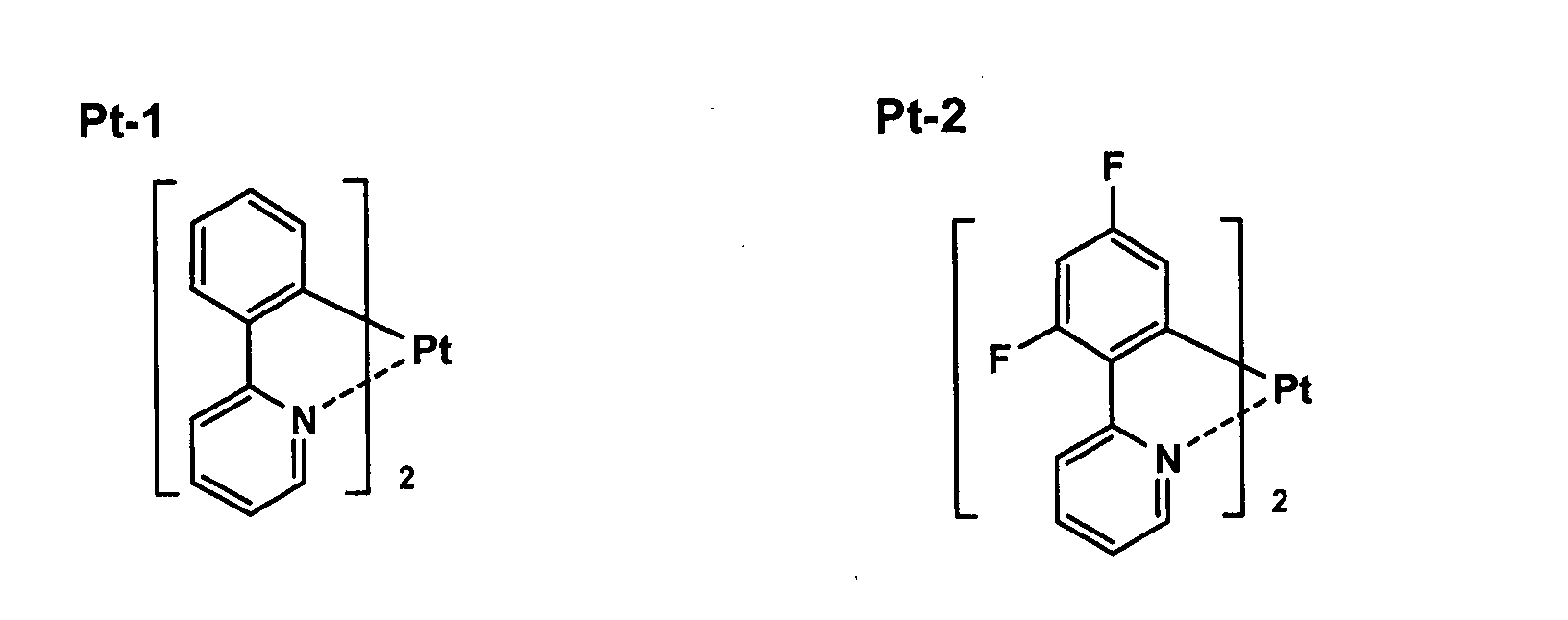
- organic electroluminescence element of any one of items 2-1 through 2-5 above, wherein the phosphorescent compound is an osmium complex or a platinum complex.
- the phosphorescent compound is a compound in which light is emitted through light-excited triplet state in which two electron spins are in parallel with each other.
- the phosphorescent compound in the invention is considered to form exited triplet state at room temperature (from 15 to 30° C) through energy transfer from the exited singlet state or excited triplet state of the fluorescent compound described above.
- Phosphorescent compounds have been considered to be capable of emitting phosphoresce only at a low temperature such as 77K.
- compounds capable of emitting phosphoresce at room temperature have been found, many compounds, for example, heavy metal-containing complexes such as iridium complexes, have been mainly synthesized and studied (see for example, S. Lamansky et al, J. Am. Chem. Soc., 123, pp. 4304, 2001).
- An aluminum complex having 5 ligands which has been recently noted, is used in a hole transporting layer, and markedly improves emission lifetime of an organic EL element as compared with bathocuproine, but has problem which lowers emission luminance.
- the band gap of each of the compounds constituting the element is not optimized, unless a phosphorescent compound is used in a large amount as compared with a host compound, its effect is not sufficiently exhibited.
- the present inventors have made an extensive study on an organic EL element, and as a result, they have obtained desirable result that optimization of the energy band structure of an organic EL element forms a structure sufficiently accumulating holes and electrons at their recombination regions and provides high emission luminance and long emission lifetime.
- Band gap referred to in the invention is a difference between ionization potential and electron affinity of a compound.
- the ionization potential and electron affinity are determined based on a vacuum level.
- the ionization potential is defined by energy necessary to release electrons of a compound existing in a HOMO (highest occupied molecular orbital) level to a vacuum level, while the electron affinity is defined by energy released when electrons of a compound existing in a vacuum level fall to a LUMO (lowest unoccupied molecular orbital) level and are stabilized.
- the band gap is obtained by vacuum depositing an organic compound on a glass plate to obtain a deposit layer with a thickness of 100 nm, measuring absorption spectra of the deposit layer, and determining wavelength Y (nm) at the longer absorption edge in the absorption spectra in terms of X (eV), where the following formula is used.
- X 1239.8/Y
- the ionization potential is directly measured employing a photoelectron spectroscopy, or can be also determined by correcting oxidation potential electrochemically measured to a standard electrode.
- the ionization potential of an organic compound is directly measured employing a photoelectron spectroscopy, and is defined by a value obtained by being measured employing a low energy electron spectrometer Model AC-1 manufactured by Riken Keiki Co., Ltd.
- energy level of HOMO is the same as ionization potential
- energy level of LUMO is the same as electron affinity
- the organic EL element of the invention is characterized in that it comprises a hole transporting layer, a light emission layer containing a host compound and a phosphorescent compound, a hole blocking layer, and an electron transporting layer, the host compound having a band gap of from 3.3eV to 5.0eV, and having a molecular weight of not less than 500, and relationship c ⁇ d being satisfied, wherein c (eV) represents a difference between energy level of LUMO in the hole blocking layer and energy level of LUMO in the light emission layer and d (eV) represents a difference between energy level of HOMO in the hole blocking layer and energy level of HOMO in the light emission layer.
- the molecular weight of the host compound is preferably not less than 600, and more preferably from 600 to 2000.
- c (energy level of LUMO in the hole blocking layer) - (energy level of LUMO in the light emission layer)
- d (energy level of HOMO in the hole blocking layer) - (energy level of HOMO in the light emission layer)
- the hole blocking function of the element is sufficiently performed, which contributes to improvement of emission efficiency.
- the wide band gap of the host compound contributes to improvement of emission efficiency of blue light which is a light with a shorter wavelength.
- the host compound with a molecular weight of not less than 500, and preferably not less than 600 increases heat resistance of the organic EL element and markedly increases lifetime of the organic EL element.
- the organic EL element is characterized in that it comprises a hole transporting layer containing a hole transporting material, a light emission layer containing a host compound and a phosphorescent compound, a hole blocking layer, and an electron transporting layer, a hole transporting material having a ratio N/C of a nitrogen atom number N to carbon atom number C of from 0.05 to 0.10, and relationship c ⁇ d being satisfied, wherein c (eV) represents a difference between energy level of LUMO in the hole blocking layer and energy level of LUMO in the light emission layer and d (eV) represents a difference between energy level of HOMO in the hole blocking layer and energy level of HOMO in the light emission layer.
- the hole blocking function of the element is sufficiently performed, which contributes to improvement of emission efficiency.
- the energy band structure is proper, when hole transporting function of a hole transporting material in the hole transporting layer is poor, it cannot contribute to improvement of emission efficiency.
- the present inventors have made an extensive study, and as a result, they have found that improvement of emission efficiency is realized by limiting the N/C ratio of the hole transporting material to a specific range, and completed the invention.
- the organic EL element of the invention comprises a hole transporting layer, a light emission layer containing a host compound and a phosphorescent compound, a hole blocking layer and an electron transporting layer, and is characterized in that the relationship a > b is satisfied, wherein a (eV) represents a difference between energy level of LUMO in the light emission layer and energy level of LUMO in the hole transporting layer and b (eV) represents a difference between energy level of HOMO in the light emission layer and energy level of HOMO in the hole transporting layer.
- the hole transporting layer of the element can sufficiently perform an electron blocking function.
- the light emission layer comprises a host compound and a phosphorescent compound (light emission material).
- the host compound include an aligoarylene derivative, a boron-containing compound, a styryl type compound, a triarylamine derivative, quinazoline or its derivatives, carbazole or its derivatives and triazine or its derivatives. Of these, a boron-containing compound, and carbazole or its derivatives are preferred.
- the phosphorescent compound in the invention is preferably a metal complex compound containing, as a center metal, a metal belonging to a group VIII of the periodic table, more preferably a metal complex compound containing osmium, iridium or platinum, and most preferably an iridium complex.
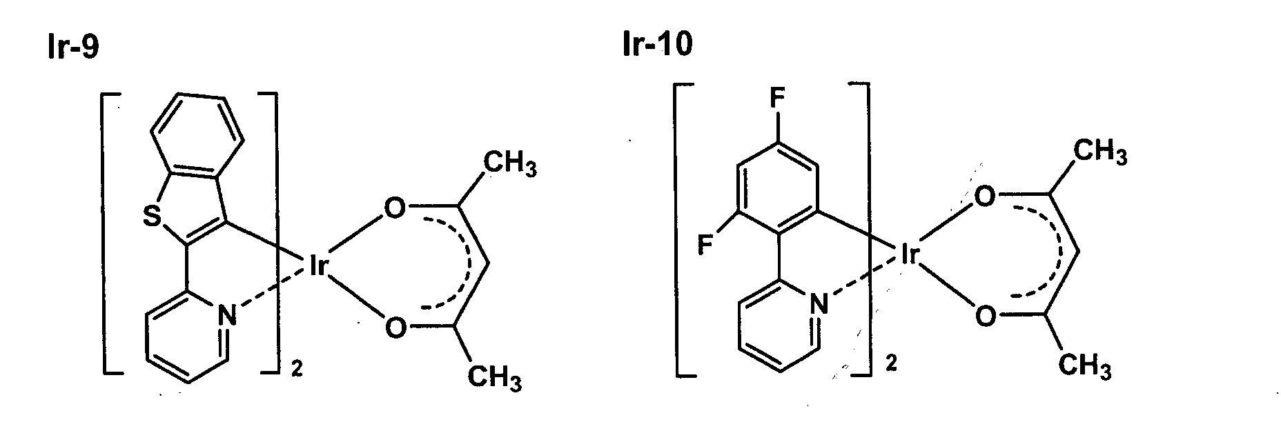
- Examples of the phosphorescent compound in the invention will be listed below, but are not limited thereto.
- the doping amount of the phosphorescent compound in the invention is from more than 0% to less than 30% by weight, preferably from 0.1% to 20% by weight, and more preferably from 6% to less than 15% by weight, based on the host compound.
- the organic EL element in the invention comprises a hole transporting layer, a light emission layer a hole blocking layer, an electron transporting layer, and optionally an anode buffer layer and a cathode buffer layer, which are provided between a cathode and an anode.
- the preferred structure of the organic EL element is shown below, but the invention is not limited thereto.
- the above light emission layer is a layer where electrons and holes, injected from electrodes, an electron transporting layer or a hole transporting layer, are recombined to emit light.
- the portions where light emits may be portions in the light emission layer or portions at the interface between the light emission layer and the layer adjacent thereto.
- the light emission materials (for example, phosphorescent compounds) of the light emission layer may have a hole transporting capability or an electron transporting capability as well as a light emission capability. Most of hole transporting materials used in the hole transporting layer, hole blocking materials used in the hole blocking layer, and electron transporting materials used in the electron transporting layer, can be used as light emission materials.
- the light emission layer can be formed employing a known method such as a vacuum deposition method, a spin coat method, a casting method and a Langumiur-Blodgett method (LB method).
- the thickness of the light emission layer is not specifically limited, but is ordinarily from 5 nm to 5 ⁇ m.
- the light emission layer may be composed of a single layer comprising one or two or more of light emission materials, or of plural layers comprising the same composition or different composition.
- the light emission layer can be formed by the method such as that described in Japanese Patent O.P.I. Publication No. 57-51781, in which a light emission material is dissolved in a solvent together with a binder such as a resin, and the thus obtained solution is formed into a thin layer by a method such as a spin-coat method. Thickness of the emission layer thus formed is not specially restricted. Although the thickness of the layer thus formed is optionally selected, the thickness is preferably within the range of from 5 nm to 5 ⁇ m.
- the hole transporting layer, hole blocking layer, and electron transporting layer will be explained below.
- the hole transporting layer has a function of transporting the hole injected from the anode to the light emission layer. Many holes can be injected in a lower electric field by the presence of the hole transporting layer between the anode and the light emission layer. Moreover, an element can be obtained which increases a light emission efficiency and has an excellent light emission ability, since the electrons injected into the light emission layer from the cathode buffer layer or the electron transporting layer are accumulated at the interface in the light emission layer by a barrier to electrons existing at the interface between the light emission layer and the hole transporting layer.
- the hole transporting material used in the hole transporting layer can be optionally selected from known materials without any limitation as far as they have the property defined in the invention. Such a material include those employed for hole injecting or transporting materials in conventional photoconductive elements or known materials used in the hole transporting layer of conventional organic EL elements.
- the hole transporting material described above may be either an organic substance or an inorganic substance as long as it has a hole transporting ability or an ability to form a barrier to electron.
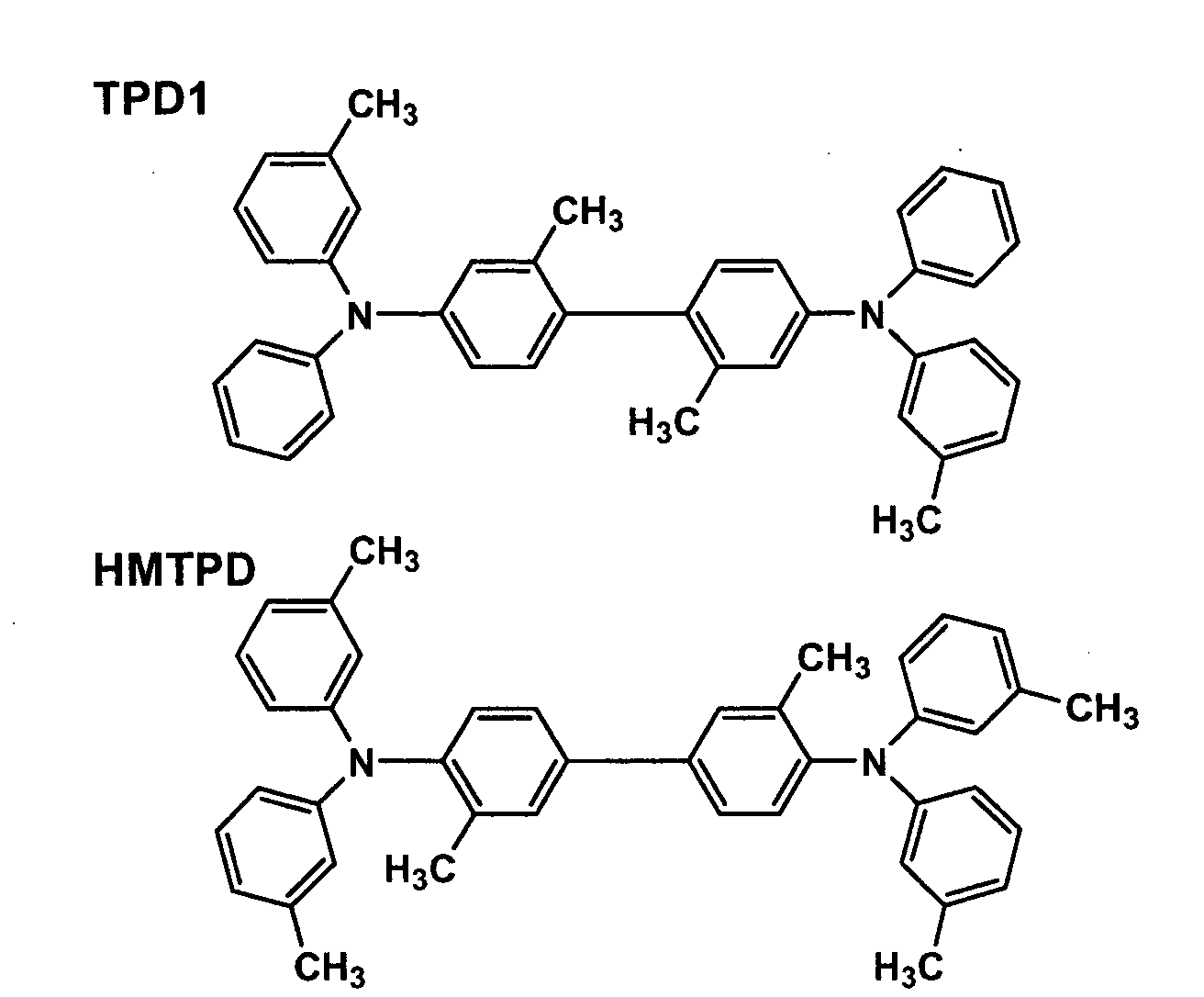
- the hole transporting material include a triazole derivative, an oxadiazole derivative, an imidazole derivative, a polyarylalkane derivative, a pyrazoline derivative and a pyrazolone derivative, a phenylenediamine derivative, an arylamine derivative, an amino substituted chalcone derivative, an oxazole derivative, a styryl anthracene derivative, a fluorenone derivative, a hydrazone derivative, a stilbene derivative, a silazane derivative, an aniline copolymer, and an electroconductive oligomer, particularly a thiophene oligomer.
- hole transporting material those described above are used, but a porphyrin compound, an aromatic tertiary amine compound, or a styrylamine compound is preferably used, and an aromatic tertiary amine compound is more preferably used.
- a polymer can be used which contains the above materials in the side chain or in the main chain.
- the hole transporting material inorganic compounds such as p-Si and p-SiC are usable.
- the hole transporting layer can be formed by layering the hole transporting material by a known method such as a vacuum deposition method, a spin coat method, a casting method and an LB method.
- the thickness of the hole transporting layer is not specifically limited, but is ordinarily from 5 nm to 5 ⁇ m.
- the hole transporting layer may be composed of a single layer comprising one or two or more of the materials mentioned above, or of plural layers comprising the same composition or different composition.
- the hole blocking layer has a function inhibiting migration of holes injected from the anode. Probability of recombination of holes and electrons is increased by the presence of the hole transporting layer between the electron transporting layer and the light emission layer, which provides an element with an excellent light emission ability increasing a light emission efficiency.
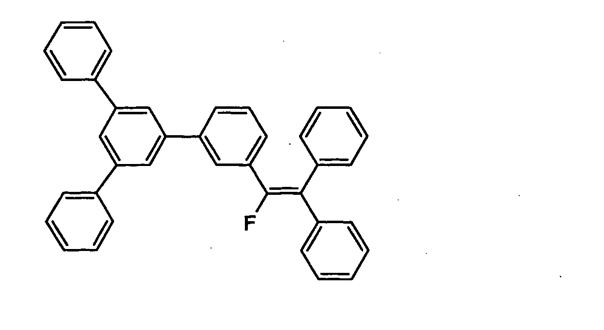
- hole blocking materials used in the hole blocking layer include phenanthroline or its derivatives, triazole or its derivatives, aluminum complex (BAlq) with 5 ligands, an aligoarylene derivative, a styryl type compound, quinazoline or its derivatives, oxadiazole or its derivatives, pyrimidine or its derivatives, triazine or its derivatives, and a boron-containing compound. Of these, phenanthroline or its derivatives, an aligoarylene derivative, a styryl type compound, quinazoline or its derivatives, and a boron-containing compound are preferred.
- the electron transporting layer has a function of transporting electrons injected to the cathode to the light emission layer. Many electrons are injected into the light emission layer at a lower electric field by the presence of the electron transporting layer between the cathode and the light emission layer.
- Examples of the electron transporting material used in the electron transporting layer include a nitro-substituted fluorene derivative, a diphenylquinone derivative, a thiopyran dioxide derivative, a heterocyclic tetracarboxylic acid anhydride such as naphthaleneperylene, a carbodiimide, a fluolenylidenemethane derivative, an anthraquinodimethane an anthrone derivative, an oxadiazole derivative, a triazole derivative and a phenanthroline derivative.
- a nitro-substituted fluorene derivative such as naphthaleneperylene, a carbodiimide, a fluolenylidenemethane derivative, an anthraquinodimethane an anthrone derivative, an oxadiazole derivative, a triazole derivative and a phenanthroline derivative.
- a thiadiazole derivative which is formed by substituting the oxygen atom in the oxadiazole ring of the foregoing oxadiazole derivative with a sulfur atom
- a quinoxaline derivative having a quinoxaline ring known as an electron withdrawing group are usable as the electron transporting material.
- a polymer can be used which contains the above materials in the side chain or in the main chain.
- a metal complex of an 8-quinolynol derivative such as aluminum tris-(8-quinolynol) (Alq 3 ), aluminum tris-(5,7-dichloro-8-quinolynol), aluminum tris-(5,7-dibromo-8-quinolynol), aluminum tris-(2-methyl-8-quinolynol), aluminum tris-(5-methyl-8-quinolynol), or zinc bis-(8-quinolynol) (Znq 2 ), and a metal complex formed by replacing the central metal of the foregoing complexes with another metal atom such as In, Mg, Cu, Ca, Sn, Ga or Pb, can be used as the electron transporting material.
- another metal atom such as In, Mg, Cu, Ca, Sn, Ga or Pb
- a metal free or metal-containing phthalocyanine, and a derivative thereof, in which the molecular terminal is replaced by a substituent such as an alkyl group or a sulfonic acid group are also preferably used as the electron transporting material.
- the distyrylpyrazine derivative exemplified as a material for the light emission layer may preferably be employed as the electron transporting material.
- An inorganic semiconductor such as n-Si and n-SiC may also be used as the electron transporting material in a similar way as in the hole transporting layer.
- An electron transporting layer can be formed by layering the compounds described above by a known method such as a vacuum deposition method, a spin coat method, a casting method and an LB method.
- the thickness of the electron transporting layer is not specifically limited, but is ordinarily from 5 nm to 5 ⁇ m.
- the electron transporting layer may be composed of a single layer comprising one or two or more of the materials mentioned above, or of plural layers comprising the same composition or different composition.
- a buffer layer (an electrode interface layer) may be provided between the anode and the hole transporting layer, or between the cathode and the electron transporting layer.
- the buffer layer is a layer provided between the electrode and an organic layer in order to reduce the driving voltage or to improve light emission efficiency.
- As the buffer layer there are an anode buffer layer and a cathode buffer layer, which are described in "Electrode Material” page 123, Div. 2 Chapter 2 of "Organic EL element and its frontier of industrialization” (published by NTS Corporation, November 30, 1998) in detail.
- the anode buffer layer is described in Japanese Patent O.P.I. Publication Nos. 9-45479, 9-260062, and 8-288069 etc., and its examples include a phthalocyanine buffer layer represented by a copper phthalocyanine layer, an oxide buffer layer represented by a vanadium oxide layer, an amorphous carbon buffer layer, a polymer buffer layer employing an electroconductive polymer such as polyaniline (emeraldine), and polythiophene, etc.
- the cathode buffer layer is described in Japanese Patent O.P.I. Publication Nos. 6-325871, 9-17574, and 9-74586, etc. in detail, and its examples include a metal buffer layer represented by a strontium or aluminum layer, an alkali metal compound buffer layer represented by a lithium fluoride layer, an alkali earth metal compound buffer layer represented by a magnesium fluoride layer, and an oxide buffer layer represented by an aluminum oxide or lithium oxide layer.
- presence of the cathode buffer layer is preferable in reducing the driving voltage or improving light emission efficiency.
- the buffer layer is preferably very thin and has a thickness of preferably from 0.1 to 100 nm depending on kinds of the material used.
- Electrodes of the organic EL element will be explained below.
- the electrodes consist of a cathode and an anode.
- a metal, an alloy, or an electroconductive compound each having a high working function (not less than 4 eV), and mixture thereof are preferably used as the electrode material.
- an electrode material include a metal such as Au, and a transparent electroconductive material such as CuI, indium tin oxide (ITO), SnO 2 , or ZnO.
- the anode may be prepared by forming a thin layer of the electrode material according to a depositing or sputtering method, and by forming the layer into a desired pattern according to a photolithographic method.
- the pattern may be formed by evaporating or sputtering of the electrode material through a mask having a desired form.
- the transmittance of the anode is preferably 10% or more, and the sheet resistivity of the anode is preferably not more than several hundred ⁇ / ⁇ .
- the thickness of the anode is ordinarily within the range of from 10 nm to 1 ⁇ m, and preferably from 10 to 200 nm, although it may vary due to kinds of materials used.
- a metal also referred to as an electron injecting metal
- an alloy also referred to as an electron injecting metal
- an electroconductive compound each having a low working function not more than 4 eV
- a mixture thereof is used as the electrode material.
- an electrode material include sodium, sodium-potassium alloy, magnesium, lithium, a magnesium/copper mixture, a magnesium/silver mixture, a magnesium/aluminum mixture, magnesium/indium mixture, an aluminum/aluminum oxide (Al 2 O 3 ) mixture, indium, a lithium/aluminum mixture, and a rare-earth metal.
- a mixture of an electron injecting metal and a metal higher in the working function than that of the electron injecting metal such as the magnesium/silver mixture, magnesium/aluminum mixture, magnesium/indium mixture, aluminum/aluminum oxide (Al 2 O 3 ) mixture or lithium/aluminum mixture, is suitable from the view point of the electron injecting ability and resistance to oxidation.
- an aluminum alloy is preferably used, and the aluminum alloy contains aluminum in an amount of preferably from 90% to less than 100% by weight, and more preferably from 95% to less than 100% by weight. This can provide an organic EL element with high luminance and long emission lifetime.
- the cathode can be prepared forming a thin layer of such an electrode material by a method such as a deposition or sputtering method.
- the sheet resistivity of the cathode is preferably not more than several hundred ⁇ / ⁇ , and the thickness of the cathode is ordinarily from 10 nm to 1 ⁇ m, and preferably from 50 to 2,00 nm. It is preferable in increasing the light emission efficiency that either the anode or the cathode of the organic EL element is transparent or translucent.
- a substrate preferably employed for the organic electroluminescence element of the invention is not restricted to specific kinds of materials such as glass and plastic, as far as it is transparent.
- Examples of the substrate preferably employed used in the organic electroluminescence element of the invention include glass, quartz and light transmissible plastic film.
- Examples of the light transmissible plastic film include films such as polyethyleneterephthalate (PET), polyethylenenaphthalate (PEN), polyethersulfone (PES), polyetherimide, polyetheretherketone, polyphenylenesulfide, polyarylate, polycarbonate (PC), cellulose triacetate (TAC), cellulose acetate propionate (CAP) and so on.
- PET polyethyleneterephthalate
- PEN polyethylenenaphthalate
- PES polyethersulfone
- PES polyetherimide
- polyetheretherketone polyphenylenesulfide
- PC polycarbonate
- TAC cellulose triacetate
- CAP cellulose acetate propionate
- a thin layer of a desired material for electrode such as a material of the anode is formed on a suitable substrate by a deposition or sputtering method, so that the thickness of the layer is not more than 1 ⁇ m, and preferably within the range of from 10 to 200 nm to prepare the anode. Then, the hole transporting layer, the light emission layer, the hole blocking layer, the electron transporting layer and the cathode buffer layer are formed on the resulting anode in that order.
- a spin coating method for forming the layers described above, there are a spin coating method, a casting method and a deposition method.
- a vacuum deposition method or a spin coat method is preferable since a uniform layer can be formed and a pinhole is formed with difficulty.
- Different layer forming methods may be used on forming different layers.
- the vacuum deposition is preferably carried out at a boat temperature of from 50° C to 450° C, at a vacuum degree of from 10 -6 to 10 -3 Pa, at a deposition speed of from 0.01 to 50 nm/second, and at a substrate temperature of from -50 to 300° C, to form a layer thickness of from 5 nm to 5 ⁇ m.
- a layer comprising a material for cathode is formed thereon by, for example, a deposition method or sputtering method so that the thickness is not more than 1 ⁇ m, and preferably from 50 to 200 nm, to provide the cathode.
- a desired organic EL element is obtained.
- the layers from the hole injecting layer to the cathode are continuously formed under one time of vacuuming to prepare the organic EL element.
- a different layer formation method may be inserted. When the different layer formation method is used, the method is required to be carried out under a dry inert gas atmosphere.
- the organic EL element can be prepared in the reverse order, in which the cathode, the cathode buffer layer, electron transporting layer, the hole blocking layer, the light emission layer, the hole transporting layer, and the anode are formed in that order.
- Light emission can be observed when a direct current with a voltage of from about 5 to 40 V is applied to the thus prepared organic EL element so that the polarity of the anode is positive and that of the cathode is negative.
- the voltage is applied in the reverse polarity, no current is formed and light is not emitted at all.
- an alternating current is applied, light is emitted only when the polarity of the node is positive and that of the cathode is negative.
- the shape of the wave of the alternating current may be optionally selected.
- the organic EL element of the invention may be used as a lamp such as a room light or a light source for exposure, a projection device projecting an image or a display directly viewing a still image or a moving image.
- the driving method may be either a simple matrix (passive matrix) method or an active matrix method.
- a full color display can be prepared.
- a pattern was formed on a substrate (manufactured by NH Technoglass Co., Ltd.) composed of a glass plate and a 150 nm ITO (indium tin oxide) layer as an anode. Then the resulting transparent substrate having the ITO transparent electrode was subjected to ultrasonic washing in i-propyl alcohol and dried by a dry nitrogen gas and subjected to UV-ozone cleaning for 5 minutes. Thus obtained transparent substrate was fixed on a substrate holder of a vacuum deposition apparatus available in the market.
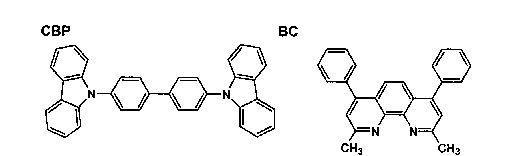
- a heating boat carrying CBP and a heating boat carrying exemplified compound Ir-10 were independently heated by supplying an electric current to both boats to deposit CBP and Ir-10 onto the hole transporting layer at a depositing speed ratio of CBP to Ir-10 of 100:6 to form a light emission layer with a thickness of 30 nm.
- a heating boat carrying BC was heated by supplying an electric current to form a hole blocking layer with a thickness of 10 nm, and a heating boat carrying Alq 3 was heated by supplying an electric current to form thereon an electron transporting with a thickness of 20 nm. Further, 1 nm lithium fluoride layer was deposited on the electron transporting layer and a 100 nm aluminum layer was provided on the lithium fluoride layer. Thus, organic EL element sample OLED 1 (comparative) was prepared. This element sample emitted blue light resulting from Ir-10.
- Organic EL element samples OLED 2 through 18 were prepared in the same manner as comparative organic EL element sample OLED 1, except that compound ⁇ -NPD in the hole transporting layer, host compound CBP in the light emission layer or compound BC in the hole blocking layer was replaced with those as shown in Table 1.
- N/C represents a nitrogen atom number in the hole transporting material/a carbon atom number in the hole transporting material
- "a” represents (a LUMO energy level (eV) in the light emission layer - a LUMO energy level (eV) in the hole transporting layer)
- "b” represents (a HOMO energy level (eV) in the light emission layer - a HOMO energy level (eV) in the hole transporting layer)
- c represents (a LUMO energy level (eV) in the hole blocking layer - a LUMO energy level (eV) in the light emission layer)
- “d” represents (a HOMO energy level (eV) in the hole blocking layer - a HOMO energy level (eV) in the light emission layer).
- luminance (cd/m 2 ) of light emitted from the sample and time (hereinafter referred to also as luminance half-life) taken until the luminance was reduced to half were measured.
- the luminance of light emitted from the organic EL element sample Nos. 2 through 18 was expressed by a relative value (hereinafter referred to also as relative luminance) when the luminance of light emitted from the organic EL element sample No. 1 was set at 100.
- inventive organic electroluminescence element samples comprising the hole transporting material in the invention, the light emission material in the invention, and the hole blocking material in the invention exhibited an excellent result in luminance and emission lifetime, compared with comparative samples.
- Organic EL element samples OLED 7G through OLED 18G were prepared in the same manner as in organic EL element samples OLED 7 through OLED 18 of Example 1, respectively, except that Ir-1 was used instead of Ir-10. Further, organic EL element samples OLED 7R through OLED 18R were prepared in the same manner as in organic EL element samples OLED 7 through OLED 18 of Example 1, respectively, except that Ir-9 was used instead of Ir-10. The resulting samples were evaluated for luminance and luminance half-life in the same manner as in Example 1. As a result, inventive organic electroluminescence element samples exhibited an excellent result in luminance and emission lifetime. Green light was emitted from the samples employing Ir-1, and red light was emitted from the samples employing Ir-9.
- the present invention can provide an organic electroluminescence element with excellent luminance and with long lifetime.
Landscapes
- Chemical & Material Sciences (AREA)
- Physics & Mathematics (AREA)
- Optics & Photonics (AREA)
- Crystallography & Structural Chemistry (AREA)
- Inorganic Chemistry (AREA)
- Engineering & Computer Science (AREA)
- Materials Engineering (AREA)
- Electroluminescent Light Sources (AREA)
Abstract
Description





| Compound | Energy level (eV) | |
| HOMO | LUMO | |
| α-NPD | 5.4 | 2.3 |
| HMTPD | 5.4 | 2.1 |
| m-MTDATXA | 5.4 | 2.2 |
| TPD1 | 5.6 | 2.3 |
| TPD2 | 5.7 | 2.1 |
| CBP | 6.0 | 2.9 |
| BC | 6.4 | 2.9 |
| TAZ | 6.4 | 2.4 |
| TCTA | 5.9 | 2.7 |
| Compound 1 | 6.4 | 2.6 |
| Compound 2 | 6.0 | 2.6 |
| Compound 3 | 6.1 | 2.5 |
| Compound 4 | 5.7 | 2.5 |
| Compound 5 | 6.5 | 2.6 |
| Compound 6 | 6.5 | 2.5 |
| Alq3 | 5.8 | 3.1 |


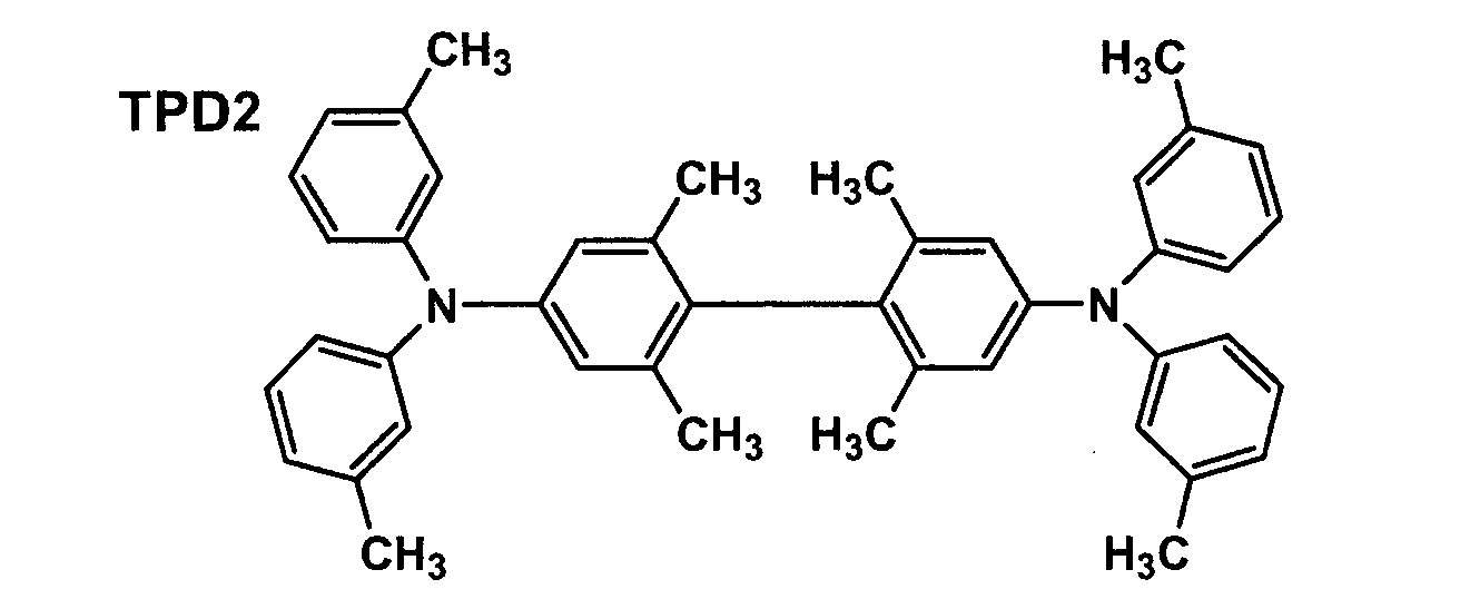
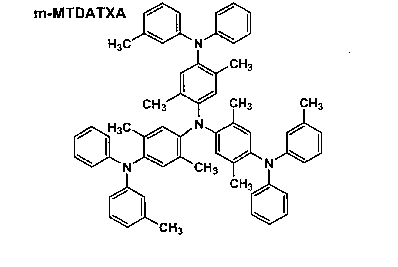
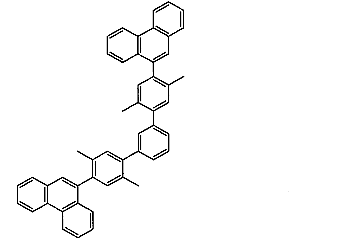
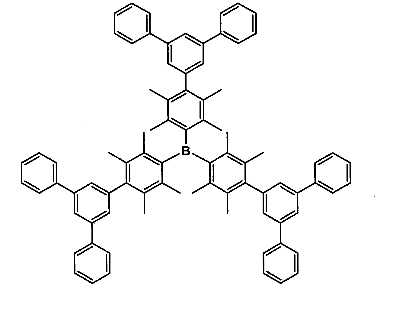



| Sample No. | Evaluation results | Remarks | |
| Relative luminance | Relative luminance half-life | ||
| 1 | 100 | 100 | Comparative |
| 2 | 105 | 80 | Comparative |
| 3 | 105 | 83 | Comparative |
| 4 | 110 | 107 | Comparative |
| 5 | 112 | 100 | Comparative |
| 6 | 110 | 95 | Comparative |
| 7 | 148 | 172 | Invention |
| 8 | 145 | 153 | Invention |
| 9 | 149 | 190 | Invention |
| 10 | 155 | 170 | Invention |
| 11 | 149 | 173 | Invention |
| 12 | 141 | 148 | Invention |
| 13 | 144 | 145 | Invention |
| 14 | 158 | 195 | Invention |
| 15 | 160 | 194 | Invention |
| 16 | 150 | 162 | Invention |
| 17 | 163 | 170 | Invention |
| 18 | 165 | 173 | Invention |
Claims (15)
- An organic electroluminescence element comprising a hole transporting layer containing a hole transporting material, a light emission layer containing a host compound and a phosphorescent compound, a hole blocking layer, and an electron transporting layer, the host compound having a band gap of from 3.3eV to 5.0eV, and having a molecular weight of not less than 500, and relationship c < d being satisfied, wherein c (eV) represents a difference between energy level of LUMO (lowest unoccupied molecular orbital) in the hole blocking layer and energy level of LUMO in the light emission layer and d (eV) represents a difference between energy level of HOMO (highest occupied molecular orbital) in the hole blocking layer and energy level of HOMO in the light emission layer.
- The organic electroluminescence element of claim 1 wherein the hole transporting material has a ratio N/C of a nitrogen atom number N to carbon atom number C of from 0.05 to 0.10.
- The organic electroluminescence element of claim 1 or 2, wherein relationship 0.0 < c/d < 0.4 is satisfied.
- The organic electroluminescence element of claim 1, 2 or 3, in which relationship a > b is satisfied, wherein a (eV) represents a difference between energy level of LUMO in the light emission layer and energy level of LUMO in the hole transporting layer and b (eV) represents a difference between energy level of HOMO in the light emission layer and energy level of HOMO in the hole transporting layer.
- The organic electroluminescence element of claim 4, wherein relationship a ≥ b + 0.2 is satisfied.
- The organic electroluminescence element of claim 1 or 2 to 5, wherein the phosphorescent compound is an iridium complex, an osmium complex or a platinum complex.
- The organic electroluminescence element of claim 6, wherein the phosphorescent compound is an iridium complex.
- The organic electroluminescence element of claim 6, wherein the phosphorescent compound is an osmium complex or a platinum complex.
- An organic electroluminescence element comprising a hole transporting layer containing a hole transporting material, a light emission layer containing a host compound and a phosphorescent compound, a hole blocking layer, and an' electron transporting layer, the hole transporting material having a ratio N/C of a nitrogen atom number N to a carbon atom number C of from 0.05 to 0.10, and relationship c < d being satisfied, wherein c (eV) represents a difference between energy level of LUMO (lowest unoccupied molecular orbital) in the hole blocking layer and energy level of LUMO in the light emission layer and d (eV) represents a difference between energy level of HOMO (highest occupied molecular orbital) in the hole blocking layer and energy level of HOMO in the light emission layer.
- The organic electroluminescence element of claim 9, wherein relationship 0.0 < c/d < 0.4 is satisfied.
- The organic electroluminescence element of claim 9 or 10, in which relationship a > b is satisfied, wherein a (eV) represents a difference between energy level of LUMO in the light emission layer and energy level of LUMO in the hole transporting layer and b (eV) represents a difference between energy level of HOMO in the light emission layer and energy level of HOMO in the hole transporting layer.
- The organic electroluminescence element of claim 11, wherein relationship a ≥ b + 0.2 is satisfied.
- The organic electroluminescence element of claim 9, 10 or 11, wherein the phosphorescent compound is an iridium complex, an osmium complex or a platinum complex.
- The organic electroluminescence element of claim 13, wherein the phosphorescent compound is an iridium complex.
- The organic electroluminescence element of claim 13, wherein the phosphorescent compound is an osmium complex or a platinum complex.
Priority Applications (1)
| Application Number | Priority Date | Filing Date | Title |
|---|---|---|---|
| EP10154244.7A EP2192632B1 (en) | 2002-04-12 | 2003-04-03 | Organic Electroluminescence Element |
Applications Claiming Priority (2)
| Application Number | Priority Date | Filing Date | Title |
|---|---|---|---|
| JP2002110303 | 2002-04-12 | ||
| JP2002110303 | 2002-04-12 |
Related Child Applications (2)
| Application Number | Title | Priority Date | Filing Date |
|---|---|---|---|
| EP10154244.7A Division EP2192632B1 (en) | 2002-04-12 | 2003-04-03 | Organic Electroluminescence Element |
| EP10154244.7A Previously-Filed-Application EP2192632B1 (en) | 2002-04-12 | 2003-04-03 | Organic Electroluminescence Element |
Publications (3)
| Publication Number | Publication Date |
|---|---|
| EP1353388A2 true EP1353388A2 (en) | 2003-10-15 |
| EP1353388A3 EP1353388A3 (en) | 2007-11-28 |
| EP1353388B1 EP1353388B1 (en) | 2010-03-17 |
Family
ID=28449982
Family Applications (2)
| Application Number | Title | Priority Date | Filing Date |
|---|---|---|---|
| EP10154244.7A Expired - Lifetime EP2192632B1 (en) | 2002-04-12 | 2003-04-03 | Organic Electroluminescence Element |
| EP03007431A Expired - Lifetime EP1353388B1 (en) | 2002-04-12 | 2003-04-03 | Organic electroluminescence element |
Family Applications Before (1)
| Application Number | Title | Priority Date | Filing Date |
|---|---|---|---|
| EP10154244.7A Expired - Lifetime EP2192632B1 (en) | 2002-04-12 | 2003-04-03 | Organic Electroluminescence Element |
Country Status (3)
| Country | Link |
|---|---|
| US (2) | US7128982B2 (en) |
| EP (2) | EP2192632B1 (en) |
| DE (1) | DE60331704D1 (en) |
Cited By (9)
| Publication number | Priority date | Publication date | Assignee | Title |
|---|---|---|---|---|
| WO2004095598A3 (en) * | 2003-04-21 | 2005-05-19 | Univ Princeton | Organic light emitting devices with wide gap host materials |
| WO2005054403A1 (en) * | 2003-12-05 | 2005-06-16 | Merck Patent Gmbh | Organic electroluminescent element |
| WO2005096403A3 (en) * | 2004-03-31 | 2006-03-02 | Matsushita Electric Industrial Co Ltd | Organic photoelectric conversion element utilizing an inorganic buffer layer placed between an electrode and the active material |
| US7180110B2 (en) | 2003-07-08 | 2007-02-20 | Matsushita Electric Industrial Co., Ltd. | Organic photoelectric conversion element |
| US7371469B2 (en) * | 2003-07-08 | 2008-05-13 | Konica Minolta Holdings, Inc. | Organic electroluminescent element, illuminator and display |
| US7956206B2 (en) | 2004-05-24 | 2011-06-07 | Cambridge Display Technology Limited | Metal complex |
| CN109148704A (en) * | 2018-08-20 | 2019-01-04 | 纳晶科技股份有限公司 | Quanta point electroluminescent device and preparation method thereof |
| CN109671851A (en) * | 2017-10-16 | 2019-04-23 | 北京鼎材科技有限公司 | A kind of organic electroluminescence device |
| CN114447238A (en) * | 2020-10-30 | 2022-05-06 | 财团法人纺织产业综合研究所 | Electroluminescent wire |
Families Citing this family (32)
| Publication number | Priority date | Publication date | Assignee | Title |
|---|---|---|---|---|
| US6660410B2 (en) * | 2000-03-27 | 2003-12-09 | Idemitsu Kosan Co., Ltd. | Organic electroluminescence element |
| EP2192632B1 (en) * | 2002-04-12 | 2014-09-03 | Konica Corporation | Organic Electroluminescence Element |
| US7416791B1 (en) * | 2002-06-11 | 2008-08-26 | University Of Washington | Osmium complexes and related organic light-emitting devices |
| EP2248870B1 (en) * | 2002-11-26 | 2018-12-26 | Konica Minolta Holdings, Inc. | Organic electroluminscent element and display and illuminator |
| US7485376B2 (en) * | 2003-03-26 | 2009-02-03 | Konica Minolta Holdings, Inc. | Organic electroluminescent element, illuminator, and display |
| US20040209115A1 (en) * | 2003-04-21 | 2004-10-21 | Thompson Mark E. | Organic light emitting devices with wide gap host materials |
| US7571894B2 (en) * | 2003-04-28 | 2009-08-11 | Fuji Photo Film Co., Ltd. | Organic electroluminescence element |
| JP4651918B2 (en) * | 2003-05-21 | 2011-03-16 | 東北パイオニア株式会社 | Manufacturing method of organic EL panel |
| WO2005026144A1 (en) | 2003-09-12 | 2005-03-24 | Sumitomo Chemical Company, Limited | Dendrimer compound and organic luminescent element employing the same |
| DE602004025026D1 (en) * | 2003-10-29 | 2010-02-25 | Philips Intellectual Property | LIGHT-OUTDOOR UNIT WITH IMPROVED QUANTUM EFFORT |
| DE10356099A1 (en) * | 2003-11-27 | 2005-07-07 | Covion Organic Semiconductors Gmbh | Organic electroluminescent element |
| US20050123796A1 (en) * | 2003-12-05 | 2005-06-09 | Giesen David J. | Organic element for electroluminescent devices |
| JP4352008B2 (en) * | 2004-03-10 | 2009-10-28 | 富士フイルム株式会社 | Light emitting element |
| US8049407B2 (en) * | 2004-09-15 | 2011-11-01 | Fujifilm Corporation | Organic electroluminescent element including blue phosphorescent luminescent material |
| WO2007020718A1 (en) * | 2005-08-18 | 2007-02-22 | Konica Minolta Holdings, Inc. | Organic electroluminescent element, display device, and lighting device |
| JPWO2007029402A1 (en) * | 2005-09-08 | 2009-03-12 | 出光興産株式会社 | Organic electroluminescence device |
| US7651791B2 (en) * | 2005-12-15 | 2010-01-26 | Idemitsu Kosan Co., Ltd. | Material for organic electroluminescence device and electroluminescence device employing the same |
| KR100774200B1 (en) * | 2006-04-13 | 2007-11-08 | 엘지전자 주식회사 | Organic EL element and its manufacturing method |
| US20080286610A1 (en) * | 2007-05-17 | 2008-11-20 | Deaton Joseph C | Hybrid oled with fluorescent and phosphorescent layers |
| US20080284318A1 (en) * | 2007-05-17 | 2008-11-20 | Deaton Joseph C | Hybrid fluorescent/phosphorescent oleds |
| WO2009051248A1 (en) * | 2007-10-19 | 2009-04-23 | Semiconductor Energy Laboratory Co., Ltd. | Light-emitting element, light-emitting device, and electronic device |
| WO2009084546A1 (en) | 2007-12-27 | 2009-07-09 | Nippon Steel Chemical Co., Ltd. | Compound for organic electroluminescent device and organic electroluminescent device using the same |
| US8324800B2 (en) * | 2008-06-12 | 2012-12-04 | Global Oled Technology Llc | Phosphorescent OLED device with mixed hosts |
| DE102008063490B4 (en) * | 2008-12-17 | 2023-06-15 | Merck Patent Gmbh | Organic electroluminescent device and method for adjusting the color locus of a white-emitting electroluminescent device |
| JPWO2011071169A1 (en) * | 2009-12-11 | 2013-04-22 | 三菱化学株式会社 | Organic electroluminescent device, organic EL display device, and organic EL lighting |
| US8242489B2 (en) | 2009-12-17 | 2012-08-14 | Global Oled Technology, Llc. | OLED with high efficiency blue light-emitting layer |
| JP4637271B1 (en) | 2010-01-15 | 2011-02-23 | 富士フイルム株式会社 | Organic electroluminescence device |
| JP2012033918A (en) | 2010-07-08 | 2012-02-16 | Mitsubishi Chemicals Corp | Organic electroluminescent element, organic electroluminescent device, organic el display device, and organic el lighting |
| KR20220025211A (en) * | 2013-07-30 | 2022-03-03 | 메르크 파텐트 게엠베하 | Materials for electronic devices |
| CN105408448B (en) * | 2013-07-30 | 2018-11-02 | 默克专利有限公司 | Materials for Electronic Devices |
| KR102794156B1 (en) | 2019-01-09 | 2025-04-14 | 삼성디스플레이 주식회사 | Organic electroluminescence device and display device including the same |
| CN112687811B (en) * | 2019-10-17 | 2023-09-12 | 北京夏禾科技有限公司 | An organic electroluminescent device |
Citations (4)
| Publication number | Priority date | Publication date | Assignee | Title |
|---|---|---|---|---|
| JPH08109373A (en) | 1994-10-13 | 1996-04-30 | Nec Corp | Organic thin film EL device |
| JPH10233284A (en) | 1997-02-19 | 1998-09-02 | Oki Electric Ind Co Ltd | Organic EL device |
| JP2001028405A (en) | 1999-07-15 | 2001-01-30 | Matsushita Electronics Industry Corp | Semiconductor device electrical characteristic evaluation apparatus |
| WO2001008230A1 (en) | 1999-07-21 | 2001-02-01 | The Trustees Of Princeton University | Intersystem crossing agents for efficient utilization of excitons in organic light emitting devices |
Family Cites Families (18)
| Publication number | Priority date | Publication date | Assignee | Title |
|---|---|---|---|---|
| US4356429A (en) | 1980-07-17 | 1982-10-26 | Eastman Kodak Company | Organic electroluminescent cell |
| JP2814435B2 (en) | 1987-03-02 | 1998-10-22 | イーストマン・コダック・カンパニー | Electroluminescent device with improved thin film emission band |
| JP2815472B2 (en) | 1990-01-22 | 1998-10-27 | パイオニア株式会社 | EL device |
| EP0610514B1 (en) | 1992-08-28 | 2003-04-02 | Idemitsu Kosan Company Limited | Charge injection assistant and organic electroluminescence device containing the same |
| JPH06325871A (en) | 1993-05-18 | 1994-11-25 | Mitsubishi Kasei Corp | Organic electroluminescent element |
| JP3561549B2 (en) | 1995-04-07 | 2004-09-02 | 三洋電機株式会社 | Organic electroluminescence device |
| JP3529543B2 (en) | 1995-04-27 | 2004-05-24 | パイオニア株式会社 | Organic electroluminescence device |
| US5719467A (en) | 1995-07-27 | 1998-02-17 | Hewlett-Packard Company | Organic electroluminescent device |
| JPH0974586A (en) | 1995-09-05 | 1997-03-18 | Matsushita Electric Ind Co Ltd | Wireless synchronizer |
| JP3645642B2 (en) | 1996-03-25 | 2005-05-11 | Tdk株式会社 | Organic electroluminescence device |
| US5776623A (en) * | 1996-07-29 | 1998-07-07 | Eastman Kodak Company | Transparent electron-injecting electrode for use in an electroluminescent device |
| GB9810798D0 (en) * | 1998-05-20 | 1998-07-15 | Sharp Kk | Light emitting devices |
| US6097147A (en) * | 1998-09-14 | 2000-08-01 | The Trustees Of Princeton University | Structure for high efficiency electroluminescent device |
| US6939624B2 (en) * | 2000-08-11 | 2005-09-06 | Universal Display Corporation | Organometallic compounds and emission-shifting organic electrophosphorescence |
| DE10058578C2 (en) * | 2000-11-20 | 2002-11-28 | Univ Dresden Tech | Light-emitting component with organic layers |
| JP2002184581A (en) * | 2000-12-13 | 2002-06-28 | Sanyo Electric Co Ltd | Organic light emitting device |
| US6855438B2 (en) * | 2001-06-15 | 2005-02-15 | Konica Corporation | Organic electroluminescent element and full color display |
| EP2192632B1 (en) * | 2002-04-12 | 2014-09-03 | Konica Corporation | Organic Electroluminescence Element |
-
2003
- 2003-04-03 EP EP10154244.7A patent/EP2192632B1/en not_active Expired - Lifetime
- 2003-04-03 DE DE60331704T patent/DE60331704D1/en not_active Expired - Lifetime
- 2003-04-03 EP EP03007431A patent/EP1353388B1/en not_active Expired - Lifetime
- 2003-04-09 US US10/410,312 patent/US7128982B2/en not_active Expired - Lifetime
-
2006
- 2006-09-06 US US11/516,285 patent/US7592075B2/en not_active Expired - Lifetime
Patent Citations (4)
| Publication number | Priority date | Publication date | Assignee | Title |
|---|---|---|---|---|
| JPH08109373A (en) | 1994-10-13 | 1996-04-30 | Nec Corp | Organic thin film EL device |
| JPH10233284A (en) | 1997-02-19 | 1998-09-02 | Oki Electric Ind Co Ltd | Organic EL device |
| JP2001028405A (en) | 1999-07-15 | 2001-01-30 | Matsushita Electronics Industry Corp | Semiconductor device electrical characteristic evaluation apparatus |
| WO2001008230A1 (en) | 1999-07-21 | 2001-02-01 | The Trustees Of Princeton University | Intersystem crossing agents for efficient utilization of excitons in organic light emitting devices |
Non-Patent Citations (2)
| Title |
|---|
| "Twelfth OyobutsuriGakkai Gakujutsukoen Kai Yokoshu 12-a-M7", PIONEER GIJUTSU JOHOSHI, vol. 11, no. 1 |
| S. LAMANSKY ET AL., J. AM. CHEM. SOC., vol. 123, 2001, pages 4304 |
Cited By (13)
| Publication number | Priority date | Publication date | Assignee | Title |
|---|---|---|---|---|
| WO2004095598A3 (en) * | 2003-04-21 | 2005-05-19 | Univ Princeton | Organic light emitting devices with wide gap host materials |
| US7180110B2 (en) | 2003-07-08 | 2007-02-20 | Matsushita Electric Industrial Co., Ltd. | Organic photoelectric conversion element |
| US7371469B2 (en) * | 2003-07-08 | 2008-05-13 | Konica Minolta Holdings, Inc. | Organic electroluminescent element, illuminator and display |
| US7981522B2 (en) | 2003-12-05 | 2011-07-19 | Merck Patent Gmbh | Organic electroluminescent element |
| WO2005054403A1 (en) * | 2003-12-05 | 2005-06-16 | Merck Patent Gmbh | Organic electroluminescent element |
| KR101153765B1 (en) * | 2003-12-05 | 2012-06-13 | 메르크 파텐트 게엠베하 | Organic electroluminescent element |
| WO2005096403A3 (en) * | 2004-03-31 | 2006-03-02 | Matsushita Electric Industrial Co Ltd | Organic photoelectric conversion element utilizing an inorganic buffer layer placed between an electrode and the active material |
| US7956206B2 (en) | 2004-05-24 | 2011-06-07 | Cambridge Display Technology Limited | Metal complex |
| CN109671851A (en) * | 2017-10-16 | 2019-04-23 | 北京鼎材科技有限公司 | A kind of organic electroluminescence device |
| CN109671851B (en) * | 2017-10-16 | 2021-10-22 | 北京鼎材科技有限公司 | An organic electroluminescent device |
| CN109148704A (en) * | 2018-08-20 | 2019-01-04 | 纳晶科技股份有限公司 | Quanta point electroluminescent device and preparation method thereof |
| CN114447238A (en) * | 2020-10-30 | 2022-05-06 | 财团法人纺织产业综合研究所 | Electroluminescent wire |
| CN114447238B (en) * | 2020-10-30 | 2024-02-02 | 财团法人纺织产业综合研究所 | Electroluminescent wire |
Also Published As
| Publication number | Publication date |
|---|---|
| EP2192632B1 (en) | 2014-09-03 |
| US20070015008A1 (en) | 2007-01-18 |
| EP2192632A1 (en) | 2010-06-02 |
| EP1353388A3 (en) | 2007-11-28 |
| DE60331704D1 (en) | 2010-04-29 |
| US20030198831A1 (en) | 2003-10-23 |
| EP1353388B1 (en) | 2010-03-17 |
| US7592075B2 (en) | 2009-09-22 |
| US7128982B2 (en) | 2006-10-31 |
Similar Documents
| Publication | Publication Date | Title |
|---|---|---|
| US7128982B2 (en) | Organic electroluminescence element | |
| US6750608B2 (en) | Organic electroluminescence element and display | |
| US6835473B2 (en) | Organic electroluminescence element and display | |
| EP2762546B1 (en) | Organic electroluminescent element, and display and illuminator | |
| US6818325B2 (en) | Light-emitting device | |
| US6982179B2 (en) | Structure and method of fabricating organic devices | |
| US8377575B2 (en) | Organic electroluminescence device | |
| US7608993B2 (en) | Blue organic electroluminescent device comprising dopants having ultraviolet and visible luminescent properties | |
| US20050242346A1 (en) | Very low voltage, high efficiency pholed in a p-i-n structure | |
| US20040209117A1 (en) | Organic light emitting devices | |
| US20050194892A1 (en) | OLEDs with mixed host emissive layer | |
| EP1653784B1 (en) | Organic electroluminescent device, illuminating device, and display | |
| US20080268285A1 (en) | Organic electroluminescent device | |
| JP2004006287A (en) | Organic electroluminescence device | |
| EP1267428B1 (en) | Organic electroluminescent element and full color display | |
| EP1665897B1 (en) | Electroluminescent device | |
| EP1652241A1 (en) | Organic electroluminescent device | |
| CN101213684A (en) | organic electroluminescent element | |
| US7935432B2 (en) | Organic electroluminescent device | |
| US20070108898A1 (en) | Organic electroluminescence device |
Legal Events
| Date | Code | Title | Description |
|---|---|---|---|
| PUAI | Public reference made under article 153(3) epc to a published international application that has entered the european phase |
Free format text: ORIGINAL CODE: 0009012 |
|
| AK | Designated contracting states |
Kind code of ref document: A2 Designated state(s): AT BE BG CH CY CZ DE DK EE ES FI FR GB GR HU IE IT LI LU MC NL PT RO SE SI SK TR |
|
| AX | Request for extension of the european patent |
Extension state: AL LT LV MK |
|
| PUAL | Search report despatched |
Free format text: ORIGINAL CODE: 0009013 |
|
| AK | Designated contracting states |
Kind code of ref document: A3 Designated state(s): AT BE BG CH CY CZ DE DK EE ES FI FR GB GR HU IE IT LI LU MC NL PT RO SE SI SK TR |
|
| AX | Request for extension of the european patent |
Extension state: AL LT LV MK |
|
| 17P | Request for examination filed |
Effective date: 20080502 |
|
| AKX | Designation fees paid |
Designated state(s): DE GB |
|
| 17Q | First examination report despatched |
Effective date: 20080805 |
|
| GRAP | Despatch of communication of intention to grant a patent |
Free format text: ORIGINAL CODE: EPIDOSNIGR1 |
|
| RIC1 | Information provided on ipc code assigned before grant |
Ipc: H01L 51/00 20060101AFI20090930BHEP |
|
| GRAS | Grant fee paid |
Free format text: ORIGINAL CODE: EPIDOSNIGR3 |
|
| GRAA | (expected) grant |
Free format text: ORIGINAL CODE: 0009210 |
|
| AK | Designated contracting states |
Kind code of ref document: B1 Designated state(s): DE GB |
|
| REG | Reference to a national code |
Ref country code: GB Ref legal event code: FG4D |
|
| REF | Corresponds to: |
Ref document number: 60331704 Country of ref document: DE Date of ref document: 20100429 Kind code of ref document: P |
|
| PLBE | No opposition filed within time limit |
Free format text: ORIGINAL CODE: 0009261 |
|
| STAA | Information on the status of an ep patent application or granted ep patent |
Free format text: STATUS: NO OPPOSITION FILED WITHIN TIME LIMIT |
|
| 26N | No opposition filed |
Effective date: 20101220 |
|
| PGFP | Annual fee paid to national office [announced via postgrant information from national office to epo] |
Ref country code: DE Payment date: 20170329 Year of fee payment: 15 |
|
| REG | Reference to a national code |
Ref country code: DE Ref legal event code: R119 Ref document number: 60331704 Country of ref document: DE |
|
| PG25 | Lapsed in a contracting state [announced via postgrant information from national office to epo] |
Ref country code: DE Free format text: LAPSE BECAUSE OF NON-PAYMENT OF DUE FEES Effective date: 20181101 |
|
| PGFP | Annual fee paid to national office [announced via postgrant information from national office to epo] |
Ref country code: GB Payment date: 20210318 Year of fee payment: 19 |
|
| REG | Reference to a national code |
Ref country code: GB Ref legal event code: 732E Free format text: REGISTERED BETWEEN 20220217 AND 20220223 |
|
| GBPC | Gb: european patent ceased through non-payment of renewal fee |
Effective date: 20220403 |
|
| PG25 | Lapsed in a contracting state [announced via postgrant information from national office to epo] |
Ref country code: GB Free format text: LAPSE BECAUSE OF NON-PAYMENT OF DUE FEES Effective date: 20220403 |