EP1351797B1 - Method for fabricating a plastic optic element injection mold - Google Patents
Method for fabricating a plastic optic element injection mold Download PDFInfo
- Publication number
- EP1351797B1 EP1351797B1 EP02705775A EP02705775A EP1351797B1 EP 1351797 B1 EP1351797 B1 EP 1351797B1 EP 02705775 A EP02705775 A EP 02705775A EP 02705775 A EP02705775 A EP 02705775A EP 1351797 B1 EP1351797 B1 EP 1351797B1
- Authority
- EP
- European Patent Office
- Prior art keywords
- positive
- mold
- line
- shell
- masters
- Prior art date
- Legal status (The legal status is an assumption and is not a legal conclusion. Google has not performed a legal analysis and makes no representation as to the accuracy of the status listed.)
- Expired - Lifetime
Links
Images


Classifications
-
- B—PERFORMING OPERATIONS; TRANSPORTING
- B29—WORKING OF PLASTICS; WORKING OF SUBSTANCES IN A PLASTIC STATE IN GENERAL
- B29C—SHAPING OR JOINING OF PLASTICS; SHAPING OF MATERIAL IN A PLASTIC STATE, NOT OTHERWISE PROVIDED FOR; AFTER-TREATMENT OF THE SHAPED PRODUCTS, e.g. REPAIRING
- B29C33/00—Moulds or cores; Details thereof or accessories therefor
- B29C33/38—Moulds or cores; Details thereof or accessories therefor characterised by the material or the manufacturing process
-
- B—PERFORMING OPERATIONS; TRANSPORTING
- B23—MACHINE TOOLS; METAL-WORKING NOT OTHERWISE PROVIDED FOR
- B23P—METAL-WORKING NOT OTHERWISE PROVIDED FOR; COMBINED OPERATIONS; UNIVERSAL MACHINE TOOLS
- B23P15/00—Making specific metal objects by operations not covered by a single other subclass or a group in this subclass
- B23P15/007—Making specific metal objects by operations not covered by a single other subclass or a group in this subclass injection moulding tools
-
- C—CHEMISTRY; METALLURGY
- C25—ELECTROLYTIC OR ELECTROPHORETIC PROCESSES; APPARATUS THEREFOR
- C25D—PROCESSES FOR THE ELECTROLYTIC OR ELECTROPHORETIC PRODUCTION OF COATINGS; ELECTROFORMING; APPARATUS THEREFOR
- C25D1/00—Electroforming
- C25D1/10—Moulds; Masks; Masterforms
-
- Y—GENERAL TAGGING OF NEW TECHNOLOGICAL DEVELOPMENTS; GENERAL TAGGING OF CROSS-SECTIONAL TECHNOLOGIES SPANNING OVER SEVERAL SECTIONS OF THE IPC; TECHNICAL SUBJECTS COVERED BY FORMER USPC CROSS-REFERENCE ART COLLECTIONS [XRACs] AND DIGESTS
- Y10—TECHNICAL SUBJECTS COVERED BY FORMER USPC
- Y10T—TECHNICAL SUBJECTS COVERED BY FORMER US CLASSIFICATION
- Y10T29/00—Metal working
- Y10T29/49—Method of mechanical manufacture
- Y10T29/49789—Obtaining plural product pieces from unitary workpiece
- Y10T29/49796—Coacting pieces
-
- Y—GENERAL TAGGING OF NEW TECHNOLOGICAL DEVELOPMENTS; GENERAL TAGGING OF CROSS-SECTIONAL TECHNOLOGIES SPANNING OVER SEVERAL SECTIONS OF THE IPC; TECHNICAL SUBJECTS COVERED BY FORMER USPC CROSS-REFERENCE ART COLLECTIONS [XRACs] AND DIGESTS
- Y10—TECHNICAL SUBJECTS COVERED BY FORMER USPC
- Y10T—TECHNICAL SUBJECTS COVERED BY FORMER US CLASSIFICATION
- Y10T29/00—Metal working
- Y10T29/49—Method of mechanical manufacture
- Y10T29/4981—Utilizing transitory attached element or associated separate material
-
- Y—GENERAL TAGGING OF NEW TECHNOLOGICAL DEVELOPMENTS; GENERAL TAGGING OF CROSS-SECTIONAL TECHNOLOGIES SPANNING OVER SEVERAL SECTIONS OF THE IPC; TECHNICAL SUBJECTS COVERED BY FORMER USPC CROSS-REFERENCE ART COLLECTIONS [XRACs] AND DIGESTS
- Y10—TECHNICAL SUBJECTS COVERED BY FORMER USPC
- Y10T—TECHNICAL SUBJECTS COVERED BY FORMER US CLASSIFICATION
- Y10T29/00—Metal working
- Y10T29/49—Method of mechanical manufacture
- Y10T29/49826—Assembling or joining
- Y10T29/49893—Peripheral joining of opposed mirror image parts to form a hollow body
-
- Y—GENERAL TAGGING OF NEW TECHNOLOGICAL DEVELOPMENTS; GENERAL TAGGING OF CROSS-SECTIONAL TECHNOLOGIES SPANNING OVER SEVERAL SECTIONS OF THE IPC; TECHNICAL SUBJECTS COVERED BY FORMER USPC CROSS-REFERENCE ART COLLECTIONS [XRACs] AND DIGESTS
- Y10—TECHNICAL SUBJECTS COVERED BY FORMER USPC
- Y10T—TECHNICAL SUBJECTS COVERED BY FORMER US CLASSIFICATION
- Y10T29/00—Metal working
- Y10T29/49—Method of mechanical manufacture
- Y10T29/4998—Combined manufacture including applying or shaping of fluent material
- Y10T29/49982—Coating
- Y10T29/49986—Subsequent to metal working
-
- Y—GENERAL TAGGING OF NEW TECHNOLOGICAL DEVELOPMENTS; GENERAL TAGGING OF CROSS-SECTIONAL TECHNOLOGIES SPANNING OVER SEVERAL SECTIONS OF THE IPC; TECHNICAL SUBJECTS COVERED BY FORMER USPC CROSS-REFERENCE ART COLLECTIONS [XRACs] AND DIGESTS
- Y10—TECHNICAL SUBJECTS COVERED BY FORMER USPC
- Y10T—TECHNICAL SUBJECTS COVERED BY FORMER US CLASSIFICATION
- Y10T29/00—Metal working
- Y10T29/49—Method of mechanical manufacture
- Y10T29/4998—Combined manufacture including applying or shaping of fluent material
- Y10T29/49988—Metal casting
- Y10T29/49989—Followed by cutting or removing material
-
- Y—GENERAL TAGGING OF NEW TECHNOLOGICAL DEVELOPMENTS; GENERAL TAGGING OF CROSS-SECTIONAL TECHNOLOGIES SPANNING OVER SEVERAL SECTIONS OF THE IPC; TECHNICAL SUBJECTS COVERED BY FORMER USPC CROSS-REFERENCE ART COLLECTIONS [XRACs] AND DIGESTS
- Y10—TECHNICAL SUBJECTS COVERED BY FORMER USPC
- Y10T—TECHNICAL SUBJECTS COVERED BY FORMER US CLASSIFICATION
- Y10T29/00—Metal working
- Y10T29/49—Method of mechanical manufacture
- Y10T29/49995—Shaping one-piece blank by removing material
Definitions
- the present invention relates to the field of injection molding, and more specifically to a method of preparing a mold suitable for forming plastic optic components.
- Thick non-imaging optics such as collimation and concentration non-imaging optics, are expensive because they are typically fabricated by machining glass. These thick non-imaging optics are typically characterized by a high aspect ratio and a number of extremely tight tolerances, including surface finish, flatness, concentricity, and perpendicularity. The cost of these optic elements can be reduced considerably by replacing the machined glass components with molded plastic components.
- plastic optic elements can be molded, for example by injection molding, when the part geometry lends itself to molding. It is also known that manufacturing the molds for high aspect ratio plastic optic parts is extremely difficult.
- US-A-2243521 describes a method of fabricating a mold comprising forming a model of the component to be produced; forming a metal shell on the model; cutting the shell along a delineating line; and combining the resulting two metal shell portions to form the mold.
- Our invention is a method for manufacturing molds suitable for the fabrication of optical components using injection-molded plastic as defined in independent claim 1. Preferred embodiments are defined in the dependent claims.
- the injection molding materials that are suitable for use with our invention include but are not limited to cyclo-olefin polymer, clear acrylic resin, and polystyrene.
- metal positive masters of the plastic optic element are first carefully machined to the exact dimensions of the desired plastic optic elements, but with adjustments to the dimensions to compensate for the determined rate of shrinkage, during curing, of the plastic when it is injected into the finished mold.
- two such machined positive masters are employed.
- Each of these positive masters then has coated thereon shells, as by electroforming, which shells conform exactly to the dimensions of the positive masters.
- more than two machined positive masters and their corresponding shells are employed.
- each shell including its encased positive master is then scribed on its outside with two lines, the first a delineating line which, in one embodiment, splits the shell in two parts.
- the axial line may not split the shell into two equal size parts.
- the second scribed line is offset slightly from the first, being below the delineating line for a first of the shells and above the delineating line for the other of these shells.
- the shells are then cut along these second scribed lines, and the portion of the positive master away from the delinearing line and between the second cutting line together with the outer shell formed thereon is then discarded.
- a pair of exact models or duplicate positive masters of the desired plastic optic component are fabricated (step 11), for example by machining a steel mandrel.
- a first and second set of negative master segments are fabricated (steps 12 and 13), for example by electroforming shells around a first and second set of positive masters and then removing and trimming these electroformed shells in accordance with our invention.
- a mold is built up (step 14) using the resulting first and second set of negative master segments.
- plastic is injected into the mold (step 15), the plastic allowed to cure (step 16), and the finished optical part is removed (step 17).
- each duplicate positive master is machined (step 112) from a metal mandrel, such as steel or copper, to the modified dimensions of the finished optical part and polished to an optical surface finish (step 114), for example eighty (80) angstroms root-mean square (RMS) microroughness.
- a steel mandrel is first diamond-turned on a lathe and then coated with a second metal (step 113), such as copper, before polishing (step 114).
- the metal model or positive master is placed in an electroforming bath (step 121) and is plated with a first hard plating metal to a predetermined thickness (step 122).
- the positive master is plated with nickel to a plating thickness of 0.625 millimeters (0.025 inches).
- the resulting combination of the positive master and its electroformed shell 51 are shown in FIG. 5.
- FIG. 5 shows the mechanical arrangement of the first negative master segment and also continue to refer to FIG. 3.
- An electroformed shell 51 has been formed about a first positive master.
- the electroformed shell 51 is scribed (step 123) with a delineating line 52 and then also scribed (step 124) with a cutting line 65, thereby defining a first negative master segment 63.
- the first negative master segment 63 is that portion of the electroformed shell 51 located above the delineating line 52.
- a discard portion 64 of the electroformed shell 51 is located below the cutting line 65, and there is an overlap region 67 which is that portion of the electroformed shell 51 located between the delineating line 52 and the cutting line 65.
- the positive master including its electroformed shell 51 is cut (step 125) at the cutting line 65 using, for example, wire-electrical discharge machining (EDM) and the discard portion 64 of the electroformed shell as well as the underlying discard region 62 of the positive master are removed and discarded.
- EDM wire-electrical discharge machining
- the upper portion of the positive master includes both the desired negative master or shell section 63 together with its encased positive master model portion 61 as well as the overlap region 67 and the portion of the outer shell 63 between the delineating line 52 and the cutting line 65.
- the outer shell section 63 of the mold is then removed from the retained and overlap portions, 61 and 67, of the model or positive master. Finally, that part of the outer shell 63 between the cutting line 65 and the delineating line 52 is trimmed away, so that the remaining upper portion of the positive master or shell is exactly one half of the desired final mold.
- any distortion of the mold shell section 63 due to the cutting operation is confined to that portion of the shell section 63 adjacent the overlap region 67, which section has been trimmed away.
- the second or lower negative master segment 73 is fabricated in a manner similar to the first negative master segment 63, with the exception that the second negative master segment 73 represents the opposite side of the optical component that will be molded. Fabricating the second negative master segment is accomplished by placing a positive master or metal model in an electroforming bath (step 131), plating an electroformed shell about the positive master (step 132), scribing a delineating line 52 (step 133) and a cutting line 75 (step 134), cutting at the cutting line (step 135) and then trimming the second negative master segment to the delineating line (step 136). Finally, just as described above, the second negative master segment 73 is separated from second retained region 72 of the positive master using techniques that are known in the art.
- FIG. 7 depicts the steps of building up the mold for the optical component.
- Many optical components may be molded simultaneously.
- a plurality of upper negative mold segments are fastened (step 141) to a molding fixture and a plurality of lower negative mold segments are fastened (step 142) to the molding fixture.
- an upper negative master mold segment 63 fabricated from a first positive master using the steps depicted in FIG. 3, and a lower negative master mold segment 73, fabricated from a second positive master using the steps depicted in FIG. 4, together completely define the finished optical component when combined together.
- a typical high aspect ratio optical component that may be fabricated using our invention is a square-to-round morphing collimator 80.
- These square-to-round morphing collimators 80 may be closely packed into array 90 and are especially useful for efficiently coupling round fiber optic cables into non-imaging outputs.
- Each of these morphing collimators 80 includes a round entrance, a square exit, a high aspect ratio of length to width, and critical optical tolerances.
- these morphing collimators 80 and other similar optical components can be molded from components from a variety of materials as cyclo-olefin polymer, clear acrylic resin, and polystyrene.
- molding plastic optic components from plastic using the methods of our invention, is considerably less expensive than machining such components from glass.
Landscapes
- Engineering & Computer Science (AREA)
- Chemical & Material Sciences (AREA)
- Mechanical Engineering (AREA)
- Chemical Kinetics & Catalysis (AREA)
- Electrochemistry (AREA)
- Materials Engineering (AREA)
- Metallurgy (AREA)
- Organic Chemistry (AREA)
- Manufacturing & Machinery (AREA)
- Moulds For Moulding Plastics Or The Like (AREA)
- Injection Moulding Of Plastics Or The Like (AREA)
- Processing And Handling Of Plastics And Other Materials For Molding In General (AREA)
Abstract
Description
- The present invention relates to the field of injection molding, and more specifically to a method of preparing a mold suitable for forming plastic optic components.
- Thick non-imaging optics, such as collimation and concentration non-imaging optics, are expensive because they are typically fabricated by machining glass. These thick non-imaging optics are typically characterized by a high aspect ratio and a number of extremely tight tolerances, including surface finish, flatness, concentricity, and perpendicularity. The cost of these optic elements can be reduced considerably by replacing the machined glass components with molded plastic components.
- It is known in the art that such plastic optic elements can be molded, for example by injection molding, when the part geometry lends itself to molding. It is also known that manufacturing the molds for high aspect ratio plastic optic parts is extremely difficult.
- There is a need for a method of producing molds suitable for injection molding fabrication of plastic optic components.
- US-A-2243521 describes a method of fabricating a mold comprising forming a model of the component to be produced; forming a metal shell on the model; cutting the shell along a delineating line; and combining the resulting two metal shell portions to form the mold.
- Our invention is a method for manufacturing molds suitable for the fabrication of optical components using injection-molded plastic as defined in independent claim 1. Preferred embodiments are defined in the dependent claims. The injection molding materials that are suitable for use with our invention include but are not limited to cyclo-olefin polymer, clear acrylic resin, and polystyrene.
- To fabricate the injection mold for a plastic optic element in accordance with our invention, metal positive masters of the plastic optic element are first carefully machined to the exact dimensions of the desired plastic optic elements, but with adjustments to the dimensions to compensate for the determined rate of shrinkage, during curing, of the plastic when it is injected into the finished mold. Specifically, to fabricate the injection mold for the plastic optic part, two such machined positive masters are employed. Each of these positive masters then has coated thereon shells, as by electroforming, which shells conform exactly to the dimensions of the positive masters. In further embodiments of our invention, more than two machined positive masters and their corresponding shells are employed.
- In accordance with an aspect of our invention, each shell including its encased positive master is then scribed on its outside with two lines, the first a delineating line which, in one embodiment, splits the shell in two parts. Depending on the shape of the plastic optic element to be molded, the axial line may not split the shell into two equal size parts. The second scribed line is offset slightly from the first, being below the delineating line for a first of the shells and above the delineating line for the other of these shells. The shells are then cut along these second scribed lines, and the portion of the positive master away from the delinearing line and between the second cutting line together with the outer shell formed thereon is then discarded.
- What remains are two shell sections slightly larger than the dimensions of the desired plastic optic part with a part of the metal model still in these shell sections. Accordingly, in the next step, the remaining part of the positive master in the shell together with that portion of the shell between the delineating line and the second cutting line are then removed from each shell section. While the cutting operation along the scribed cutting lines may distort the dimensions of the outer shell adjacent to these cutting lines, in accordance with our invention, because the cutting of the shell is done away from the delineating line, the cutting operation will not affect the desired dimensions of the finished mold when the two mold half shell sections are then joined together to form the finished injection mold.
-
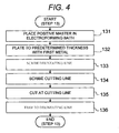
- FIG. 1 is a flow chart illustrating the general procedure for manufacturing a mold for a high aspect ratio plastic optical part in accordance with the present invention.
- FIGS. 2, 3, and 4 illustrate specific details of the procedure of FIG. 1, in accordance with the present invention.
- FIG. 5 depicts a machined mandrel with an electroformed shell surrounding the mandrel and illustrating a first discard region, in accordance with an illustrative embodiment of our invention.
- FIG. 6 depicts a machined mandrel with an electroformed shell surrounding the mandrel and illustrating a second discard region, in accordance with an illustrative embodiment of our invention.
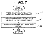
- FIG. 7 illustrates specific details of the procedure of FIG. 1, in accordance with the present invention.
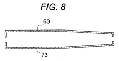
- FIG. 8 depicts two halves of an injection mold that have been prepared from two separate negative masters in accordance with an illustrative embodiment of our invention.
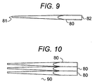
- FIG. 9 illustrates a round-to-square morphing collimator, an example of a high aspect ratio plastic optical part fabricated by our inventive process.
- FIG. 10 illustrates the high aspect ratio optical parts of FIG. 9 arranged in an illustrative useful configuration.
- Referring first to FIG. 1, the steps for manufacturing a high aspect ratio plastic optical part using a mold fabricated in accordance with our invention are shown. First, a pair of exact models or duplicate positive masters of the desired plastic optic component are fabricated (step 11), for example by machining a steel mandrel. Next, a first and second set of negative master segments are fabricated (
steps 12 and 13), for example by electroforming shells around a first and second set of positive masters and then removing and trimming these electroformed shells in accordance with our invention. Next, a mold is built up (step 14) using the resulting first and second set of negative master segments. Finally, plastic is injected into the mold (step 15), the plastic allowed to cure (step 16), and the finished optical part is removed (step 17). - The detailed steps of fabricating the duplicate positive masters are shown in FIG. 2. First, the design dimensions of the finished optical part are modified (step 111), using computer-aided design (CAD) techniques, to take into account the shrinkage of the plastic material, such as cyro-acrylic, during curing. Each duplicate positive master is machined (step 112) from a metal mandrel, such as steel or copper, to the modified dimensions of the finished optical part and polished to an optical surface finish (step 114), for example eighty (80) angstroms root-mean square (RMS) microroughness. In one embodiment, a steel mandrel is first diamond-turned on a lathe and then coated with a second metal (step 113), such as copper, before polishing (step 114).
- Referring now to FIG. 3 the detailed steps of fabricating the first negative master segment are shown. The metal model or positive master is placed in an electroforming bath (step 121) and is plated with a first hard plating metal to a predetermined thickness (step 122). In one embodiment of our inventive, the positive master is plated with nickel to a plating thickness of 0.625 millimeters (0.025 inches). The resulting combination of the positive master and its
electroformed shell 51 are shown in FIG. 5. - Refer now to FIG. 5, which shows the mechanical arrangement of the first negative master segment and also continue to refer to FIG. 3. An
electroformed shell 51 has been formed about a first positive master. Theelectroformed shell 51 is scribed (step 123) with adelineating line 52 and then also scribed (step 124) with acutting line 65, thereby defining a firstnegative master segment 63. In the embodiment illustrated in FIG. 5, the firstnegative master segment 63 is that portion of theelectroformed shell 51 located above thedelineating line 52. Adiscard portion 64 of theelectroformed shell 51 is located below thecutting line 65, and there is anoverlap region 67 which is that portion of theelectroformed shell 51 located between thedelineating line 52 and thecutting line 65. - Next, the positive master including its
electroformed shell 51 is cut (step 125) at thecutting line 65 using, for example, wire-electrical discharge machining (EDM) and thediscard portion 64 of the electroformed shell as well as the underlyingdiscard region 62 of the positive master are removed and discarded. - At this point in our inventive process, the upper portion of the positive master includes both the desired negative master or
shell section 63 together with its encased positivemaster model portion 61 as well as theoverlap region 67 and the portion of theouter shell 63 between thedelineating line 52 and thecutting line 65. Theouter shell section 63 of the mold is then removed from the retained and overlap portions, 61 and 67, of the model or positive master. Finally, that part of theouter shell 63 between thecutting line 65 and thedelineating line 52 is trimmed away, so that the remaining upper portion of the positive master or shell is exactly one half of the desired final mold. - By cutting along the scribed
cutting line 65, and not along thedelineating line 52, any distortion of themold shell section 63 due to the cutting operation is confined to that portion of theshell section 63 adjacent theoverlap region 67, which section has been trimmed away. - Referring next to FIGS. 4 and 6, the second or lower
negative master segment 73 is fabricated in a manner similar to the firstnegative master segment 63, with the exception that the secondnegative master segment 73 represents the opposite side of the optical component that will be molded. Fabricating the second negative master segment is accomplished by placing a positive master or metal model in an electroforming bath (step 131), plating an electroformed shell about the positive master (step 132), scribing a delineating line 52 (step 133) and a cutting line 75 (step 134), cutting at the cutting line (step 135) and then trimming the second negative master segment to the delineating line (step 136). Finally, just as described above, the secondnegative master segment 73 is separated from second retainedregion 72 of the positive master using techniques that are known in the art. - Refer next to FIG. 7, which depicts the steps of building up the mold for the optical component. Many optical components may be molded simultaneously. A plurality of upper negative mold segments are fastened (step 141) to a molding fixture and a plurality of lower negative mold segments are fastened (step 142) to the molding fixture. Sprues and gates added (step 143) as required, using techniques that are known in the field.
- Referring now to FIG. 8, an upper negative
master mold segment 63, fabricated from a first positive master using the steps depicted in FIG. 3, and a lower negativemaster mold segment 73, fabricated from a second positive master using the steps depicted in FIG. 4, together completely define the finished optical component when combined together. - Finally referring to FIGS. 9 and 10, a typical high aspect ratio optical component that may be fabricated using our invention is a square-to-
round morphing collimator 80. These square-to-round morphing collimators 80 may be closely packed intoarray 90 and are especially useful for efficiently coupling round fiber optic cables into non-imaging outputs. Each of these morphingcollimators 80 includes a round entrance, a square exit, a high aspect ratio of length to width, and critical optical tolerances. As described above, these morphingcollimators 80 and other similar optical components can be molded from components from a variety of materials as cyclo-olefin polymer, clear acrylic resin, and polystyrene. - Advantageously, molding plastic optic components from plastic, using the methods of our invention, is considerably less expensive than machining such components from glass.
- There are embodiments of the invention wherein more than two metal positive masters are used to make more than two negative mold segments.
Claims (10)
- A method for fabricating an injection mold for a plastic optical component comprising the steps of:a) forming at least two metal positive masters of the plastic optical component to be produced by the mold;b) forming a metal shell (51) on each of said positive masters;c) defining a delineating line (52) through each of said shells, each line delineating upper and lower portions of each shell;d) cutting one of said shells and an underlying one of said positive masters along a cutting line (75) above its delineating line and the other of said shells and an underlying other of said positive masters along a cutting line (65) below its delineating line;e) discarding the portion of the metal shell and the portion of the positive master from its cutting line away from its delineating line for each of said shells;f) removing the positive master from the remainder of the shell and trimming the portion (67,77) of the shell between its cutting line and its delineating line for each of said shells; andg) combining the resulting metal shell portions (63,73) to form the injection mold.
- The method in accordance with claim 1 wherein the step of forming said positive master includes the steps of:determining the shrinkage rate of the plastic to be molded; andadjusting the dimensions of said positive masters accordingly.
- The method in accordance with claim 1 wherein the step of forming at least two positive masters comprises the steps of:fabricating a plurality of duplicate positive masters of the optical component from a first metal;polishing each of said plurality of duplicate positive masters to an optical surface finish;placing each of said duplicate positive masters in an electroforming bath; andelectroforming a shell (51) of a second metal on each of said duplicate positive masters to a predetermined thickness.
- The method in accordance with claim 3 wherein said cutting step comprises cutting each of a set of positive masters along a cutting line (65,75) to form a set of negative master segments, wherein each of said negative master segments comprises a portion of the electroforming shell about a positive master.
- The method in accordance with claim 4 wherein said trimming step comprises removing an overlapping region comprising a portion (67,77) of the electroformed shell and interposed between its cutting line and its delineating line; and separating each of said positive masters from each of said negative segments to form a set of negative master mold segments.
- The method in accordance with claim 5 where said combining step comprises building up a mold from a set of negative master mold segments.
- The method in accordance with claim 6 wherein said first metal is selected from the group of copper, steel, copper-coated steel, and nickel-coated steel.
- The method in accordance with claim 7 wherein said second metal is nickel.
- The method in accordance with claim 1, wherein said mold is suitable for injection molding of plastic materials selected from the group consisting of cyclo-olefin polymer, clear acrylic resin, and polystyrene.
- The method in accordance with claim 1 wherein said step of forming a metal shell on each of said positive masters comprises electroforming.
Applications Claiming Priority (5)
| Application Number | Priority Date | Filing Date | Title |
|---|---|---|---|
| US46964 | 1987-05-06 | ||
| US26280201P | 2001-01-19 | 2001-01-19 | |
| US262802P | 2001-01-19 | ||
| US10/046,964 US6735844B2 (en) | 2001-01-19 | 2002-01-14 | Method for fabricating a plastic optic element injection mold |
| PCT/US2002/000979 WO2002068147A1 (en) | 2001-01-19 | 2002-01-15 | Method for fabricating a plastic optic element injection mold |
Publications (2)
| Publication Number | Publication Date |
|---|---|
| EP1351797A1 EP1351797A1 (en) | 2003-10-15 |
| EP1351797B1 true EP1351797B1 (en) | 2006-07-26 |
Family
ID=26724484
Family Applications (1)
| Application Number | Title | Priority Date | Filing Date |
|---|---|---|---|
| EP02705775A Expired - Lifetime EP1351797B1 (en) | 2001-01-19 | 2002-01-15 | Method for fabricating a plastic optic element injection mold |
Country Status (11)
| Country | Link |
|---|---|
| US (1) | US6735844B2 (en) |
| EP (1) | EP1351797B1 (en) |
| JP (1) | JP4088157B2 (en) |
| KR (1) | KR100830618B1 (en) |
| AT (1) | ATE333964T1 (en) |
| AU (1) | AU2002239904B8 (en) |
| CA (1) | CA2435215A1 (en) |
| DE (1) | DE60213363T2 (en) |
| IL (1) | IL157022A0 (en) |
| NZ (1) | NZ527285A (en) |
| WO (1) | WO2002068147A1 (en) |
Families Citing this family (6)
| Publication number | Priority date | Publication date | Assignee | Title |
|---|---|---|---|---|
| ATE326182T1 (en) * | 2000-02-23 | 2006-06-15 | Zeiss Carl Meditec Ag | HANDPIECE FOR RADIATION OF LIGHT ON A SURFACE OF SKIN |
| TWI290126B (en) * | 2004-08-18 | 2007-11-21 | Delta Electronics Inc | The method of die forming |
| CN1810481A (en) * | 2005-01-26 | 2006-08-02 | 鸿富锦精密工业(深圳)有限公司 | Optical lens mold core making process |
| US7916396B2 (en) * | 2008-06-27 | 2011-03-29 | Micron Technology, Inc. | Lens master devices, lens structures, imaging devices, and methods and apparatuses of making the same |
| CN108555552B (en) * | 2018-04-14 | 2020-09-15 | 华域视觉科技(上海)有限公司 | Machining process for automobile lamp die parts |
| CN112570999B (en) * | 2020-12-15 | 2022-07-01 | 苏州市跃宇精密机械有限公司 | High-precision aerospace part ultra-precision machining process |
Family Cites Families (22)
| Publication number | Priority date | Publication date | Assignee | Title |
|---|---|---|---|---|
| US1850141A (en) | 1928-08-21 | 1932-03-22 | Rosenqvist Gunnar | Method of making molds |
| US2182775A (en) * | 1937-03-17 | 1939-12-12 | Paul C Abouchar | Method of making dies |
| US2243521A (en) | 1938-08-04 | 1941-05-27 | Us Rubber Co | Electroforming method of making tire molds |
| BE512572A (en) | 1951-07-04 | |||
| US2788555A (en) * | 1952-06-25 | 1957-04-16 | Sukacev Lev | Methods of making a mold |
| US2838961A (en) * | 1954-01-20 | 1958-06-17 | John E Dalgleish | Method of making dies |
| US3285835A (en) * | 1963-04-29 | 1966-11-15 | Owens Illinois Glass Co | Method and apparatus for electroforming split glassware molds |
| US3261768A (en) * | 1965-08-05 | 1966-07-19 | Bryon J Sabin | Method of producing light modulators |
| US3784451A (en) * | 1969-06-23 | 1974-01-08 | Ici Ltd | Method of fabricating a composite mold having a resin-impregnated metal molding surface |
| US3840977A (en) * | 1973-05-08 | 1974-10-15 | P Dimitracopoulos | Method of making molds for molding or casting optical parts and the like |
| US4459880A (en) * | 1982-09-03 | 1984-07-17 | Jernberg Forgings Co. | Method of making dies |
| US4808272A (en) * | 1986-06-20 | 1989-02-28 | Spalding & Evenflo Companies, Inc. | Method of constructing a mold for making game balls |
| JPH01198494A (en) * | 1988-02-01 | 1989-08-10 | Toyota Motor Corp | Production of hot runner block |
| US5488763A (en) * | 1994-04-12 | 1996-02-06 | Chen; Chin-Jen | Method for making a mold for a lens of single lens glasses having two focal axes |
| US5837156A (en) * | 1994-04-21 | 1998-11-17 | Cumming; J. Stuart | Methods of fabricating intraocular lenses and lens molds |
| US5658515A (en) * | 1995-09-25 | 1997-08-19 | Lee; Abraham P. | Polymer micromold and fabrication process |
| JP3217999B2 (en) * | 1997-12-03 | 2001-10-15 | セイコーインスツルメンツ株式会社 | Component manufacturing method and component manufacturing device |
| US5939011A (en) * | 1998-04-06 | 1999-08-17 | Ford Global Technologies, Inc. | Method for producing a mandrel for use in hot isostatic pressed powder metallurgy rapid tool making |
| US6279425B1 (en) * | 1999-11-12 | 2001-08-28 | Edmond Burton Cicotte | Method of producing tools and dies |
| US20030146528A1 (en) * | 2002-02-01 | 2003-08-07 | Kuo-Jui Huang | Method for manufacturing microlens light guide |
| US20030164565A1 (en) * | 2002-03-04 | 2003-09-04 | O'brien Keith T. | Method of fabricating an injection mold insert for molding lens molds |
| US7029565B2 (en) * | 2002-05-24 | 2006-04-18 | Konica Corporation | Method of producing optical element forming die |
-
2002
- 2002-01-14 US US10/046,964 patent/US6735844B2/en not_active Expired - Fee Related
- 2002-01-15 EP EP02705775A patent/EP1351797B1/en not_active Expired - Lifetime
- 2002-01-15 AU AU2002239904A patent/AU2002239904B8/en not_active Ceased
- 2002-01-15 WO PCT/US2002/000979 patent/WO2002068147A1/en active IP Right Grant
- 2002-01-15 IL IL15702202A patent/IL157022A0/en unknown
- 2002-01-15 NZ NZ527285A patent/NZ527285A/en unknown
- 2002-01-15 KR KR1020037009591A patent/KR100830618B1/en not_active IP Right Cessation
- 2002-01-15 JP JP2002567494A patent/JP4088157B2/en not_active Expired - Fee Related
- 2002-01-15 CA CA002435215A patent/CA2435215A1/en not_active Abandoned
- 2002-01-15 DE DE60213363T patent/DE60213363T2/en not_active Expired - Fee Related
- 2002-01-15 AT AT02705775T patent/ATE333964T1/en not_active IP Right Cessation
Also Published As
| Publication number | Publication date |
|---|---|
| JP2004537435A (en) | 2004-12-16 |
| JP4088157B2 (en) | 2008-05-21 |
| ATE333964T1 (en) | 2006-08-15 |
| IL157022A0 (en) | 2004-02-08 |
| NZ527285A (en) | 2004-10-29 |
| CA2435215A1 (en) | 2002-09-06 |
| US6735844B2 (en) | 2004-05-18 |
| EP1351797A1 (en) | 2003-10-15 |
| AU2002239904B8 (en) | 2005-09-29 |
| KR100830618B1 (en) | 2008-05-20 |
| DE60213363T2 (en) | 2007-08-02 |
| US20020116808A1 (en) | 2002-08-29 |
| AU2002239904B2 (en) | 2005-06-02 |
| WO2002068147A1 (en) | 2002-09-06 |
| WO2002068147A8 (en) | 2002-10-24 |
| DE60213363D1 (en) | 2006-09-07 |
| KR20030071835A (en) | 2003-09-06 |
Similar Documents
| Publication | Publication Date | Title |
|---|---|---|
| CA2145683C (en) | Method of making plastic molds and process for cast molding contact lenses | |
| US4279401A (en) | Apparatus and method for making cast ophthalmic lenses | |
| US11884032B2 (en) | Production method for spectacle lens molding mold and production method for spectacle lens | |
| EP3730270A1 (en) | Production method for spectacle lens molding mold and production method for spectacle lens | |
| EP1351797B1 (en) | Method for fabricating a plastic optic element injection mold | |
| AU2002239904A1 (en) | Method for fabricating a plastic optic element injection mold | |
| JPH0484978A (en) | Manufacture of golf ball | |
| JPS6034448B2 (en) | Method for manufacturing a mold for forming the rim of eyeglasses | |
| JP2006263952A (en) | Injection molded product, and method and apparatus for manufacturing the same | |
| JPS62144908A (en) | Manufacturing method for fresnel lens molding tool | |
| US3840977A (en) | Method of making molds for molding or casting optical parts and the like | |
| JPH07223211A (en) | Manufacture of metal or ceramic powder sintered product | |
| WO2004097488A1 (en) | Method of manufacturing hybrid aspherical lens | |
| JPS5898225A (en) | Manufacture of lens system | |
| JPH08276438A (en) | Mold for fresnel lens and manufacture thereof | |
| JP3000155B2 (en) | Injection mold | |
| JPH0732369A (en) | Manufacture of resin mold | |
| JPS587330A (en) | Molding method of aspherical lens | |
| JPH03284716A (en) | Plastic-made progressive multi-focus spectacle lens and its production | |
| JPH01198494A (en) | Production of hot runner block | |
| JPS611425A (en) | Manufacture of forming metallic mold | |
| JPS6157912A (en) | Ferrule for optical connector | |
| JP2001121244A (en) | Method for manufacturing hollow decorative parts for spectacles | |
| JPS59212230A (en) | Injection molding machine | |
| JPS5872424A (en) | Manufacture of synthetic resin gear |
Legal Events
| Date | Code | Title | Description |
|---|---|---|---|
| PUAI | Public reference made under article 153(3) epc to a published international application that has entered the european phase |
Free format text: ORIGINAL CODE: 0009012 |
|
| 17P | Request for examination filed |
Effective date: 20030717 |
|
| AK | Designated contracting states |
Kind code of ref document: A1 Designated state(s): AT BE CH CY DE DK ES FI FR GB GR IE IT LI LU MC NL PT SE TR |
|
| AX | Request for extension of the european patent |
Extension state: AL LT LV MK RO SI |
|
| 17Q | First examination report despatched |
Effective date: 20041115 |
|
| GRAP | Despatch of communication of intention to grant a patent |
Free format text: ORIGINAL CODE: EPIDOSNIGR1 |
|
| GRAS | Grant fee paid |
Free format text: ORIGINAL CODE: EPIDOSNIGR3 |
|
| GRAA | (expected) grant |
Free format text: ORIGINAL CODE: 0009210 |
|
| AK | Designated contracting states |
Kind code of ref document: B1 Designated state(s): AT BE CH CY DE DK ES FI FR GB GR IE IT LI LU MC NL PT SE TR |
|
| PG25 | Lapsed in a contracting state [announced via postgrant information from national office to epo] |
Ref country code: IT Free format text: LAPSE BECAUSE OF FAILURE TO SUBMIT A TRANSLATION OF THE DESCRIPTION OR TO PAY THE FEE WITHIN THE PRESCRIBED TIME-LIMIT;WARNING: LAPSES OF ITALIAN PATENTS WITH EFFECTIVE DATE BEFORE 2007 MAY HAVE OCCURRED AT ANY TIME BEFORE 2007. THE CORRECT EFFECTIVE DATE MAY BE DIFFERENT FROM THE ONE RECORDED. Effective date: 20060726 Ref country code: NL Free format text: LAPSE BECAUSE OF FAILURE TO SUBMIT A TRANSLATION OF THE DESCRIPTION OR TO PAY THE FEE WITHIN THE PRESCRIBED TIME-LIMIT Effective date: 20060726 Ref country code: FI Free format text: LAPSE BECAUSE OF FAILURE TO SUBMIT A TRANSLATION OF THE DESCRIPTION OR TO PAY THE FEE WITHIN THE PRESCRIBED TIME-LIMIT Effective date: 20060726 Ref country code: LI Free format text: LAPSE BECAUSE OF FAILURE TO SUBMIT A TRANSLATION OF THE DESCRIPTION OR TO PAY THE FEE WITHIN THE PRESCRIBED TIME-LIMIT Effective date: 20060726 Ref country code: BE Free format text: LAPSE BECAUSE OF FAILURE TO SUBMIT A TRANSLATION OF THE DESCRIPTION OR TO PAY THE FEE WITHIN THE PRESCRIBED TIME-LIMIT Effective date: 20060726 Ref country code: CH Free format text: LAPSE BECAUSE OF FAILURE TO SUBMIT A TRANSLATION OF THE DESCRIPTION OR TO PAY THE FEE WITHIN THE PRESCRIBED TIME-LIMIT Effective date: 20060726 Ref country code: AT Free format text: LAPSE BECAUSE OF FAILURE TO SUBMIT A TRANSLATION OF THE DESCRIPTION OR TO PAY THE FEE WITHIN THE PRESCRIBED TIME-LIMIT Effective date: 20060726 |
|
| REG | Reference to a national code |
Ref country code: GB Ref legal event code: FG4D |
|
| REG | Reference to a national code |
Ref country code: CH Ref legal event code: EP |
|
| REG | Reference to a national code |
Ref country code: IE Ref legal event code: FG4D |
|
| REF | Corresponds to: |
Ref document number: 60213363 Country of ref document: DE Date of ref document: 20060907 Kind code of ref document: P |
|
| PG25 | Lapsed in a contracting state [announced via postgrant information from national office to epo] |
Ref country code: DK Free format text: LAPSE BECAUSE OF FAILURE TO SUBMIT A TRANSLATION OF THE DESCRIPTION OR TO PAY THE FEE WITHIN THE PRESCRIBED TIME-LIMIT Effective date: 20061026 Ref country code: SE Free format text: LAPSE BECAUSE OF FAILURE TO SUBMIT A TRANSLATION OF THE DESCRIPTION OR TO PAY THE FEE WITHIN THE PRESCRIBED TIME-LIMIT Effective date: 20061026 |
|
| PG25 | Lapsed in a contracting state [announced via postgrant information from national office to epo] |
Ref country code: ES Free format text: LAPSE BECAUSE OF FAILURE TO SUBMIT A TRANSLATION OF THE DESCRIPTION OR TO PAY THE FEE WITHIN THE PRESCRIBED TIME-LIMIT Effective date: 20061106 |
|
| PG25 | Lapsed in a contracting state [announced via postgrant information from national office to epo] |
Ref country code: PT Free format text: LAPSE BECAUSE OF FAILURE TO SUBMIT A TRANSLATION OF THE DESCRIPTION OR TO PAY THE FEE WITHIN THE PRESCRIBED TIME-LIMIT Effective date: 20061226 |
|
| NLV1 | Nl: lapsed or annulled due to failure to fulfill the requirements of art. 29p and 29m of the patents act | ||
| PG25 | Lapsed in a contracting state [announced via postgrant information from national office to epo] |
Ref country code: IE Free format text: LAPSE BECAUSE OF NON-PAYMENT OF DUE FEES Effective date: 20070115 |
|
| PG25 | Lapsed in a contracting state [announced via postgrant information from national office to epo] |
Ref country code: MC Free format text: LAPSE BECAUSE OF NON-PAYMENT OF DUE FEES Effective date: 20070131 |
|
| EN | Fr: translation not filed | ||
| PLBE | No opposition filed within time limit |
Free format text: ORIGINAL CODE: 0009261 |
|
| STAA | Information on the status of an ep patent application or granted ep patent |
Free format text: STATUS: NO OPPOSITION FILED WITHIN TIME LIMIT |
|
| 26N | No opposition filed |
Effective date: 20070427 |
|
| PG25 | Lapsed in a contracting state [announced via postgrant information from national office to epo] |
Ref country code: FR Free format text: LAPSE BECAUSE OF FAILURE TO SUBMIT A TRANSLATION OF THE DESCRIPTION OR TO PAY THE FEE WITHIN THE PRESCRIBED TIME-LIMIT Effective date: 20070511 Ref country code: GR Free format text: LAPSE BECAUSE OF FAILURE TO SUBMIT A TRANSLATION OF THE DESCRIPTION OR TO PAY THE FEE WITHIN THE PRESCRIBED TIME-LIMIT Effective date: 20061027 |
|
| PGFP | Annual fee paid to national office [announced via postgrant information from national office to epo] |
Ref country code: GB Payment date: 20071212 Year of fee payment: 7 |
|
| PGFP | Annual fee paid to national office [announced via postgrant information from national office to epo] |
Ref country code: DE Payment date: 20080131 Year of fee payment: 7 Ref country code: IT Payment date: 20080119 Year of fee payment: 7 |
|
| PG25 | Lapsed in a contracting state [announced via postgrant information from national office to epo] |
Ref country code: FR Free format text: LAPSE BECAUSE OF FAILURE TO SUBMIT A TRANSLATION OF THE DESCRIPTION OR TO PAY THE FEE WITHIN THE PRESCRIBED TIME-LIMIT Effective date: 20060726 |
|
| PG25 | Lapsed in a contracting state [announced via postgrant information from national office to epo] |
Ref country code: CY Free format text: LAPSE BECAUSE OF FAILURE TO SUBMIT A TRANSLATION OF THE DESCRIPTION OR TO PAY THE FEE WITHIN THE PRESCRIBED TIME-LIMIT Effective date: 20060726 Ref country code: LU Free format text: LAPSE BECAUSE OF NON-PAYMENT OF DUE FEES Effective date: 20070115 |
|
| GBPC | Gb: european patent ceased through non-payment of renewal fee |
Effective date: 20090115 |
|
| PG25 | Lapsed in a contracting state [announced via postgrant information from national office to epo] |
Ref country code: TR Free format text: LAPSE BECAUSE OF FAILURE TO SUBMIT A TRANSLATION OF THE DESCRIPTION OR TO PAY THE FEE WITHIN THE PRESCRIBED TIME-LIMIT Effective date: 20060726 |
|
| PG25 | Lapsed in a contracting state [announced via postgrant information from national office to epo] |
Ref country code: DE Free format text: LAPSE BECAUSE OF NON-PAYMENT OF DUE FEES Effective date: 20090801 |
|
| PG25 | Lapsed in a contracting state [announced via postgrant information from national office to epo] |
Ref country code: GB Free format text: LAPSE BECAUSE OF NON-PAYMENT OF DUE FEES Effective date: 20090115 |
|
| PG25 | Lapsed in a contracting state [announced via postgrant information from national office to epo] |
Ref country code: IT Free format text: LAPSE BECAUSE OF NON-PAYMENT OF DUE FEES Effective date: 20090115 |
|
| P01 | Opt-out of the competence of the unified patent court (upc) registered |
Effective date: 20230525 |