BACKGROUND OF THE INVENTION
Field of the Invention
The present invention relates to an apparatus for generating multiple
clocks from a single reference clock source.
Background Art
Electronic systems using MPEG (Moving Pictures Experts Group)
compression method for video or audio data is well known. There are several
different varieties of MPEG formats currently available. When data is
compressed using MPEG, some of the data is lost during the compression. Such
loss of data maybe attributed to different factors such as variation of components
in the system, signal jitter and others.
MPEG formats are most often used to record video or audio data of the
World Wide Web and other sources to be used for later playback. A user is often
inconvenienced by having to wait until recording of the MPEG-coded data
finishes in order to do something else with the data. The time when such
recording taking place might also be an inconvenience to the user. There is a need
to provide a better multi-functional system that will enable a user to perform
multiple functions, such as watching a movie on a cable channel, while an
MPEG-coded material is being downloaded from the Internet, or downloading an
MPEG-coded material at a preselected time other than the time it is playing.
Conventionally known systems do not allow a user to perform such
multitude of functions without increasing circuit area and power requirements.
In fact, most conventional systems have a large circuit area, require greater
operational power and produce a lot of jitter. Therefore, there is a need for a
better system that is capable of performing the above functions without increasing
circuit area and operational power.
BRIEF SUMMARY OF THE INVENTION
The present invention is a phase rotator that generates an output signal
having plurality of possible output phases with reduced jitter between the output
phase states.
The low jitter phase rotator includes a plurality of differential amplifiers
configured to receive a plurality of input differential signals having different
phases, and configured to generate a plurality of weighted signals responsive to
said plurality of input differential signals. A plurality of digital-to-analog
converters (DAC) are arranged into a plurality of groups, each group of DACs
configured to provide current for one of said corresponding differential
amplifiers. The number of active DACs in each group of DACs determines a
relative weighting of the weighted signals, where relative weighting determining
an output phase of an output signal of the phase rotator. The DACs are configured
to adjust the output phase of the phase rotator. At a kth phase, N/4 adjacent DACs
are activated that are indexed as m0, m1, ...m((N/4)-1), wherein N is the number of
said plurality of DACs. At (k+1)th phase, a m(N/4)DAC is activated that is adjacent
to the m((N/4)-1) DAC. At (k+2)th phase, the m0 DAC is de-activated.
The m0 th DAC is left active at the (k+1)th phase, and is not deactivated
until the (k+2)th. The result is that there is one more active DACs at the (k+1)th
phase than at the kth phase or the (k+2)th phase. Therefore, the gaps between the
kth, (k+1)th, and (k+2)th phase states are reduced, thereby reducing the phase jitter
of the phase rotator.
A shift register having N outputs controls the switches in the N-number
of DACs. The shift register is configured to shift N/4 bits through the N outputs,
so as to control the corresponding switches of the N number of DACs. The N/4
bits in the shift register determine the relative weighting of the weighted signals,
and thereby determine the output phase of the output signal. The N/4 bits in the
shift register are continuously shifted through the shift register, thereby causing
the output phase to rotate around an 360 degree cycle. The continuous phase
rotation causes the output signal to be frequency shifted based on the rate that the
N/4 bits are shifted through said shift register.
BRIEF DESCRIPTION OF THE DRAWINGS/FIGURES
The present invention is described with reference to the accompanying
drawings. In the drawings, like reference numbers indicate identical or
functionally similar elements. Additionally, the left most digit(s) of a reference
number identifies the drawing in which the reference number first appears.
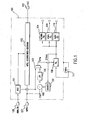
FIG. 1 is a block diagram illustrating an example environment for the
present invention may be implemented.
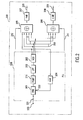
FIG. 2 is a block diagram of an embodiment of the present invention
having a PLL coupled to two phase rotators.
FIG. 3 is a more detailed block diagram of an embodiment of the present
invention illustrating a logic control circuit.
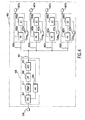
FIG. 4 is an embodiment of the present invention showing a phase locked
loop circuit coupled with four phase rotators.
FIG. 5 is a more detailed block diagram of an embodiment of the present
invention shown in FIG 2.
FIG. 6 illustrates phase locked loop circuit.
FIG. 7 illustrates is a block diagram of a 6-bit phase rotator according to
the present invention.
FIG. 8a illustrates a 4-bit phase rotator according to embodiments of the
present invention.
FIG. 8b is a more detailed illustration of an embodiment of the 4-bit phase
rotator shown in FIG. 8a.
FIG. 9 is a block diagram of an embodiment of a digital-to-analog
converter shown in FIG. 8a.
FIG. 10 is a diagram of a full phase cycle showing particular phases.
FIG. 11 is a table showing sequences representing phases generated by a
4-bit phase rotator.
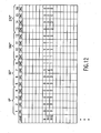
FIG. 12 is a table showing sequences representing phases generated by a
modified 4-bit phase rotator, according to embodiments of the present invention.
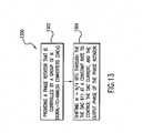
FIG. 13 is a flowchart diagram of the method of operation of the phase
rotator in the present invention.
FIG. 14 is a more detailed representation of a FIG. 13 method step of
shifting bits in the phase rotator.
DETAILED DESCRIPTION OF THE INVENTION
1. Overview
2. Phase Locked Loop Circuit
3. Multiple Synthesized Clocks with Fractional PPM Control from a Single
Clock Source
4. Phase Rotator
5. Low Jitter Phase Rotator
6. Conclusions
1. Overview
The present invention relates to systems and methods for generating
multiple clock sources from a single reference clock source. The multiple clock
sources can be coupled to output circuits that require different frequency clocks.
In an embodiment, the present invention includes plurality of phase
rotators coupled to the output of a PLL. The PLL receives a reference signal and
generates a plurality of output signals having a respective plurality of phases. The
output signals from the PLL are supplied to the plurality of phase rotators. Each
phase rotator is configured to (1) assign a relative weighting to the signals from
the PLL to form a plurality of weighted signals, and (2) combine the weighted
signals to form an output signal, wherein the relative weighting determines an
output phase of the output signal. The output phase is rotated at a continuous rate
to implement fine frequency tuning, since frequency is the derivative of phase.
The present invention may be implemented in a system, where a plurality
of audio or video equipment is coupled to the PLL. Such equipment may have
specific requirements with respect to its driving clock sources.
FIG. 1 illustrates an example environment for the present invention. The
system 100 is shown to have an analog input pad 120 and an MPEG input pad
121. Input signals having input frequency are supplied through these two pads.
The input signal received by the analog input pad 120 is processed by the video
decoder 101. The input signal received by the MPEG input pad 121 is processed
by the MPEG Decoder/Video Generator 102. The signal generated by the video
decoder 101 is also processed by the device 102. The output pad 122 receives an
output signal and is coupled to the device 102. The output signal may be in the
form of a video, audio, or other signals.
The input signals received at the input pads 120 and 121 are processed
and supplied to the system as a control signal (CPPM) signal from the multiplexor
103, where PPM represents parts per million. The CPPM signal represents a desired
frequency shift in the output of the PLL 108 in parts per million. The output of
the PLL 108 is then processed by various circuits 104, 109, and 110. For each
circuit 104, 109 and 110, the desired frequency may differ. Therefore, there is an
need for a way to generate multiple output signals having different frequencies
from a common PLL.
2. Phase Locked Loop Circuit
In an embodiment, the present invention includes a phase locked loop
(PLL) circuit. The following is a description of a PLL that may be used by the
present invention. It is understood by one skilled in the art that other types of PLL
circuits may be implemented by the present invention.
FIG. 6 illustrates a PLL 600 that is used to generate an output clock that
is frequency locked to a reference frequency that is received by the PLL 600. The
PLL 600 contains a phase detector 610, low pass filter 620, a voltage controlled
oscillator (VCO) 630, and a divider 640.
The phase detector 610 is a device that compares the phases of two input
signals, generating a phase-error output that is a measure of their difference. More
specifically, the phase detector 610 receives an input reference signal 601 at a
first input terminal 603 and a VCO feedback signal 644 at a second input terminal
604. The phase detector 610 compares the phases of the input reference signal
601 with the VCO feedback signal 644. The phase detector 610 includes a charge
pump that generates an output current 611 representative of the phase difference
between input reference signal 601 and VCO feedback signal 644.
The filter 620 low-pass filters the phase detector output 611 to remove
high frequency noise, and producing an output voltage 622. The output voltage
622 of the low pass filter 620 is the control voltage for the VCO 630.
The VCO 630 receives the control voltage 622 and generates an output
signal 633 having a frequency that is determined by the control voltage 622.
The divider circuit 640 divides the frequencies of the VCO output signal
633 so that it is consistent with the frequency of the input signal 601, generating
the VCO feedback signal 644.
3. Multiple Synthesized Clocks with Fractional PPM Control from a Single
Clock Source
The present invention relates to systems and methods for generating
multiple clock sources from a single reference clock source. The multiple clock
sources can be coupled to output circuits that require different frequency clocks.
In an embodiment, the present invention includes plurality of phase
rotators coupled to the output of a phase lock loop PLL. The PLL receives a
reference signal and generates a plurality of output signals having a respective
plurality of phases. The output signals from the PLL are supplied to the plurality
of phase rotators. Each phase rotator is configured to assign a relative weighting
to the signals from the PLL to form a plurality of weighted signals, and combine
the weighted signals to form an output signal, wherein the relative weighting
determines an output phase of the output signal. The output phase is rotated at a
continuous rate to implement fine frequency tuning, since frequency is the
derivative of phase.
FIG. 2 illustrates a system 200 for generating multiple clocks from a
single reference clock according to an embodiment of the present invention.
System 200 includes a phase locked loop circuit 108 coupled to two phase rotator
circuits 205 and 206. The phase rotators 205 and 206 are located outside the
phase lock loop 108. It is understood by one skilled in the art that any number of
phase rotator circuits may be coupled to the phase locked loop circuit 108 so as
to generate any number of output signals.
The phase locked loop circuit 108 has an input terminal 230 that receives
a reference signal 231 to the phase locked loop circuit 108. The reference signal
231 has a reference signal frequency and a reference phase.
The phase locked loop circuit 108 further has a phase detector 201, a
charge pump 211, a low pass filter 202, a voltage controlled oscillator 203, along
with a divider circuit 204. The phase detector 201 receives the reference signal
231 through its first input terminal 230 and receives a signal fed back from the
VCO 203 at its second input terminal 233. The signal received at the second input
terminal 233 is fed back by the divider circuit 204. The phase detector 201
compares frequencies of signals received at both input terminals 232 and 233, and
generates an error signal that represents the phase difference.
The charge pump 211 receives the error signal from the phase detector
201 and generates an error current that drives the low pass filter 202.
The low pass filter 202 is coupled between the output of the charge pump
211 and the voltage controlled oscillator 203. The low pass filter 202 filters the
output current from the charge pump 211 to remove high frequency noise,
producing a low frequency or DC control voltage for the VCO 203. The passband
of the filter 202 may vary according to requirements of the system 200.
The VCO 203 receives the control voltage signal from the low pass filter
202, and generates an output signal having a frequency that is tuned according to
the control voltage from the lowpass filter 202. The divider circuit 204 is coupled
between the VCO 203 output and the phase detector input terminal 233. The
divider circuit 204 divides the frequency of the VCO output signal so that it is
consistent with the frequency of the input signal 231, allowing the phase detector
201 to compare the input signal 230 to the feedback signal 233. The divider
circuit 204 has a divider ratio that can be set according to the requirements of the
system 200.
In one embodiment, the VCO 203 includes a plurality of delay cells or
buffers that are configured to oscillate. For example, the buffers can be series-connected,
where the output of the buffers is fed back in-phase to the input of the
buffers, causing the buffers to oscillate. Multiple output taps can be taken
between the buffers to generate a plurality of output signals having respective
different output phases, as represented by output signals 250 in FIG.2. Each
output signal 250 has a different output phase, and differs from the output phase
of an adjacent signal by the amount of buffer delay.
Because the VCO 203 is coupled to the divider circuit 204, the PLL is
capable of generating a multiple of the reference signal frequency 230.
The phase rotators 205 and 206 each receive the plurality of output signals
250 having corresponding different phases. The phase rotators 205 and 206 are
configured to (1) assign a relative weighting to the signals from the PLL 108 to
form a plurality of weighted signals, and (2) combine the weighted signals to
form a respective output signal, wherein the relative weighting determines an
output phase of the output signal. More specifically, the phase rotators 205 and
206 continuously rotate their respective output signals through 360 degrees with
greater resolution than that associated with the output signals 250. By
continuously rotating the output signals 250, the phase rotators 205 and 206
introduce a frequency shift in the respective output signals 220 and 221, where
the amount of frequency shift is determined by the rotation speed of the
respective phase rotator.
FIG. 10 illustrates a full phase rotation cycle of the output signal 220 (and
is also representative of the output signal 221). The phase rotator 205
continuously rotates the phase of output signal 220 around the full 360 degree
cycle. The continuous phase rotation implements a frequency shift because
frequency is the derivative of phase. As shown in FIG. 10, the phase rotation
occurs in steps or increments around the 360 cycle, where a phase state 1005 is
shown to be adjacent to a phase state 1004. A gap 1006 is formed between the
two adjacent phases 1004 and 1005. This gap 1006 represents phase jitter and
should be minimized by reducing the size of the phase steps.
In one embodiments discussed further herein, the phase rotators 205 and
206 are able to reduce the amount of the jitter in the signal by increasing the
phase resolution so that the number of phase states around the 360 degree cycle
are increased. In other words, each adjacent phase state is generated closer to the
next adjacent phase state, thereby reducing the phase jitter without increasing
circuit size or operational power. In other words, the smaller the gap 1006 (in
FIG. 10), the smaller the jitter in the system. Conversely, the larger the gap 1006,
the larger the jitter in the system.
A control signal 242, externally supplied to the phase rotator 205,
determines the rotation speed of the phase rotator 205, and therefore the
frequency shift introduced by the phase rotator 205. A divider circuit 207 receives
the output of the phase rotator 205 and divides the frequency of the output signal
of the phase rotator by the divider ratio (e.g. 48) to generate the output signal 220.
A control signal 241, externally supplied to the phase rotator 206,
determines the rotation speed of the phase rotator 206, and therefore the
frequency shift introduced by the phase rotator 206. A divider circuit 208 receives
the output of the phase rotator 206 and divides the frequency of the output signal
of the phase rotator by the divider ratio (e.g. 48) to generate the output signal 221.
FIG. 3 illustrates a logic control circuit 370 for the phase rotator 205. A
similar logic control circuit controls the phase rotator 206, but is not shown for
ease of illustration. The logic circuitry 370 includes a logic control unit 315 that
receives the control signal 242, which indicates a desired frequency shift to be
performed by the phase rotator 205. In one embodiment, the control signal 242
is a parts per million (PPM) count signal (CPPM), where CPPM represents the
amount of desired frequency shift measured in quantities of parts per million. One
PPM would represent a frequency shift of 1 Hz for every 1 MHz of output
frequency.
The CPPM signal 242 is applied to the logic control unit 315. The logic
control unit 315 is coupled with a divider circuit 371. The divider circuit 371
provides a reference clock phase to an accumulator circuit 364 within the logic
control unit 315. The frequency output of the accumulator circuit 364 is
determined by the following formula:
f 364 = ƒ371 * CPPM 211
where, f364 is an output frequency of the accumulator circuit 364, f371 is an output
frequency of the divider circuit 371, and 211 factor indicates that the accumulator
circuit 364 is an 11-bit accumulator circuit. It is understood by one skilled in the
art that the accumulator circuit 364 may an n-bit accumulator circuit.
The logic control unit 315 is further coupled to a 7-bit counter 313, 7-64
decoder 312, and a latch 311.
The phase rotator 205 generates an even greater number of phases from
the plurality of phases already generated by the phase locked loop circuit 108.
More specifically, the phase rotator 205 continuously rotates the output signals
through 360 degrees with greater resolution than that associated with the output
signals 250. By continuously rotating the output signals 250, the phase rotator
205 introduces a frequency shift in the output signals 220, where the amount of
frequency shift is determined by the rotation speed of the respective phase rotator.
The rotation speed of the phase rotator is controlled by the control signal supplied
to it by the logic circuitry 370.
The frequency of the output signals 250 are determined using the input
signal frequency 231 and an error factor. The error factor is derived from the
value of the control signal (CPPM), according to the following equations:
fOUT = fIN +CPPM 218 * ƒVCO N
where
fVCO = DividerRatio*fIN
where:
fIN is the frequency of the input signal 231 received at the input terminal
230; fOUT is the frequency of the output signal 220; and fVCO is the oscillating
frequency of the voltage controlled oscillator 203; N is a divider ratio set by the
divider circuit 371 within the logic control unit 315 (e.g., N = 64 in this
embodiment). Furthermore, the factor 218 indicates that the system comprises the
7-bit counter 313 and the 11-bit accumulator circuit 364.
The 7-bit counter 313 receives data-in bits from the logic control unit 315.
In one embodiment, the counter 313 is capable of storing a 7-bit digital word. The
7-bit counter 313 may be substituted with any other counter depending on how
many phases are generated by the phase rotator 205. Once the counter has a 7-bit
digital word formed from bits sent to it, the counter 313 forwards the digital word
to the decoder 312. The decoder 312 converts 7-bit digital word into a 64-character
sequence of 0's and 1's. The latch 311, which is also coupled to the logic
control unit 315 is preset so that when the counter 313 has a 7-bit digital word
and it is properly decoded by the decoder 312, the latch will toggle the phase
rotator 205 to increase or decrease the speed of the phase rotation, to adjusting the
frequency shift provided by the phase rotator 205.
The counter 313 receives information in bits from the logic control unit
315. Such information may be modified by the unit 315 by adding or subtracting
bits via a sign bus 325. By adding bits to the counter, the phase rotator is rotating
clockwise. By subtracting the bits from the counter, the phase rotator is rotating
counterclockwise. Referring back to FIG. 10, the clockwise rotation is shown by
a directional arrow 1011 and the counterclockwise rotation is shown by a
directional arrow 1012.
Referring back to FIG. 3, once the counter 313 has a value (i.e., a 7-bit
digital word), it would mean that the a phase rotator needs adjust its rotation
speed. After which, the counter value is reset so that the operation cycle is
changed until the counter 313 reaches the desired value.
The logic control unit 315 also includes the accumulator 364 coupled to
a timing synchronization latch 361. The accumulator 364 further comprises a
latch 362 coupled to a most significant bit (MSB) device 363. The accumulator
364 sends a MSB signal 365 to the 7-bit counter 313. The most significant bit
device 363 determines that portion of a number, address or field which occurs
leftmost when its value is written as a single number in conventional hexadecimal
or binary notation.
If the MSB device 363 determines that the first bit sent to the counter is
0, then the bits are subtracted and the phase rotator rotates counterclockwise. If
the MSB device 363 determines that the first bit is 1, then the bits are added and
the phase rotator rotates clockwise.
By supplying signal 242 to the logic control unit 315, the signal is
processed by the synchronization latch 361 and latch 362. Depending on the value
of the CPPM, the number of bits received by the 7-bit counter 313 via connection
325 is either increased or decreased. However, once the counter 313 has 7-bits of
data (according to this particular embodiment), the number of bits does not
change.
Once the 7-bit counter 313 has a count, i.e., it has received 7-bits of data
and the decoder 312 has decoded it, the latch 311 sends a signal to the phase
rotator 310 to set or adjust the rotation speed of the phase rotator 205.
In an embodiment of the present invention, the input reference signal 231
is at 27MHz. In this embodiment of the present invention, the divider ratio is 48.
Therefore, the voltage controlled oscillator 203 oscillates at approximate an
frequency of 1.3GHz. If the VCO 203 is oscillating at 1.3GHz, then the frequency
of the output signal 220 is determined using formulas (1) and (2) above. In a
particular embodiment:
fOUT = 27 MHz ± CPPM 218 *(48*27 MHZ)64
where CPPM is a programmable 12-bit digital signal. It is understood by one skilled
in the art that CPPM may assume any other value according to the requirements of
the system, as well as the divider circuit ratio 64 can be any other ratio.
Referring to FIG. 5, the present invention is shown to have a single phase
locked loop circuit 108 coupled with two phase rotator circuits 205 and 206. FIG.
5 is a more detailed representation of FIG. 2, discussed above. FIG. 5 shows
present invention's system 200. The system 200 comprises the phase locked loop
circuit 108 for receiving an input reference signal 231 at the input terminal 230.
The PLL 108 is coupled to two phase rotator circuits 205 and 206. The first phase
rotator circuit 205 is coupled to a logic control unit 518. The second phase rotator
circuit 206 is coupled to a logic control unit 519. Two CPPM signals 241 and 242
are supplied to the second and first phase rotator circuits, respectively. Each logic
control unit receives PPM count signals 241 and 242 and activates respective
phase rotators to rotate at speeds determined by the control signals 241 and 242.
The output signal having an output frequency matching the reference signal
frequency is received at output terminal 302 and is determined using formulas (1)
and (2) above.
Referring back to FIG. 2, the present invention is shown having PLL 108
coupled to two phase rotator circuits 205 and 206. It is understood by one skilled
in the art, that other combinations are possible. For example, referring to FIG. 4,
the present invention is shown as system 460. The system 460 has the phase
locked loop circuit 108 receiving an input signal at the input terminal 230. The
PLL 108 is coupled to four phase rotator circuits 465 (a, b, c, d). The PLL 108
outputs a plurality of output signals having a plurality of phases 461, which are
supplied to each of the phase rotator circuits 465 via connectors 462(a, b, c, d),
respectively.
Each phase rotator circuit 465(a, b, c, d) further coupled to a logic control
unit 466(a, b, c, d), respectively. Each logic control unit 466(a, b, c, d) is
controlled by a CPPM(a, b c, d) signal 470(a, b, c, d), respectively. The CPPM signals
activate each respective phase rotator 465(a, b, c, d) to begin generating phases,
and control the phase rotation speed, and thereby the frequency shift introduced
by each phase rotator.
4. Phase Rotator
As discussed above, the phase rotator (also called a "phase interpolator")
generates more phases out of the fixed number of phases that are received from
the phase locked loop circuit, and the phases are continuously rotated (in time)
to implemented a frequency shift in the output signal. The phases are rotated in
an incremental manner, where the difference between two phase states is referred
to as jitter, and generally should be reduced.
A rotator consists of a plurality of digital-to-analog converters (DACs)
coupled together into a group according to clock phase sources of 0°,90°,180°,
and 270°. The phase rotator operates in a full phase cycle of 360°.
Referring to FIG. 10, a full phase cycle 1000 of 360° is shown to have a
first clock phase source 1001 at 0°, a second clock phase source 1002 at 90°, a
third clock phase source 1008 at 180°, and a fourth clock phase source 1009 at
270°. Each clock phase source represents one quarter of the full phase cycle
1000. The clock phase is defined by a relationship where the frequency of a
continuously rotated signal is a derivative of the clock phase.
The number of DACs determines the phase jitter in the system. The
smaller the number of DACs, the greater the phase jitter or noise, the greater the
number of DACs the smaller the jitter. This occurs because the number of DAC
also determines the number of phase states that exist in the 360 degree rotation
cycle. The greater the number of DACs, the greater the number of phase states.
The phase jitter must be significantly reduced without increasing circuit space and
power to operate the circuit.
Referring to FIG. 10, phase jitter is represented as a gap that is formed
between two adjacent phases generated by the phase rotator. For example, if
phase represented by arrows 1004 and 1005 were adjacent phases, the gap 1006
formed between two phases would represent jitter in the system. The larger the
gap, the greater the jitter. Conversely, the smaller the gap, the smaller the jitter.
Each DAC group is controlled by a differential signal supplied to the
group. The differential signal may come from a phase locked loop circuit coupled
with the phase rotator. The PLL may have a plurality of delay cells that may be
paired up to generate a plurality of differential signals to be supplied to the phase
rotator.
A DAC comprises a switch and a current source. Whenever a current is
applied to a DAC and a switch is closed, the digital value of the DAC is 1. When
no current is applied to the DAC, the digital value of the DAC is 0. Therefore,
any data signals sent to the system will generate current and when this current is
applied to the DAC it is represented by a sequence of 0's and 1's in a digital form.
Thus, if an n-bit word is received, it is represented by a sequence of 0's and 1's.
Since the decoded digital word is represented by a binary number (0's or
1's), then the entire length of the decoded digital word may be represented by 2n,
where n is an integer. The integer n is a number of characters in a digital word
(i.e., 4-bit, 6-bit, etc.) that are decoded by the rotator's decoder. Therefore, in a 4-bit
phase rotator, n equals to 4 and the length of the digital word is 16. In a 6-bit
phase rotator, n is 6 and the length of the digital word is 64.
The number of characters that need to be decoded determines how many
bits in the decoded digital word would be 1 and how many would be 0. Therefore,
in a 4-bit rotator, in the decoded digital word of length 16, there are 4 ones and
12 zeros. Similarly, using the 6-bit rotator, 8 ones and 56 zeros are generated.
Each 1 in the decoded digital word corresponds to a DAC being turned on. This
means that the switch located in that DAC is closed and the current is supplied
to the DAC. Each 0 in the decoded digital word corresponds to a DAC being
turned off. This means that the switch located in that DAC is open and no current
is supplied to it.
Each decoded digital word represents a particular phase state of the 360
degree phase cycle that is shown in FIG.10. An output phase is determined by
computing the mean of phases defined by adjacent clock phase sources (i.e., 0°,
90°, 180°, or 270°). Therefore, if there are two phases from two adjacent clock
phase sources (e.g., 0° and 90°), then the output phase would equal to the mean
of the two phases. The following formula represents how the new output phase
ϕ0 is computed using the two phases ϕa and ϕb from two adjacent clock phase
sources:
cos(2πft + ϕ0) ≅ kN cos(2πft + ϕ a ) + (N-k)N cos(2πft + ϕb )
where k corresponds to the number of DACs that have value 1 in a particular
clock phase source (i.e., 0°, 90°, 180°, or 270°), N corresponds to the total
number of bits in the DAC (i.e., in a case of 6-bit rotator, there are 8 bits per each
clock phase source), f and t correspond to frequency and time, respectively.
In the rotator, the output phase is determined by how many DACs have
a value of 1, i.e., a current is supplied to the DAC. For instance, in a 4-bit rotator,
if first four DACs (out of 16) have a value of 1, then the output phase is
determined by the following
44 *(0°) + 04 *(90°) + 04 *(180°) + 04 *(270°) = 0°
Therefore, the output phase is 0°. In a second example, the first DAC has a value
of 0, and the following four DACs have a value equal to 1. Therefore, the output
phase is computed as follows:
Output phase = 34 *(0°) + 14 *(90°) + 04 *(180°) + 04 *(270°) = 22.5°
Therefore, the output phase is 22.5°. The output phase depends on how the
current is supplied to each digital-to-analog converter within each clock phase
source (0°,90°,180°,270°). Current supply to the DAC corresponds to the value
of 1 assigned to the DAC and in the calculation of the output phase counts
towards determination of the fraction's numerator of each clock phase source
contribution. Referring to the second example above, 3 DACs have a current
supplied to them at clock phase source of 0°, and 1 DAC has a current supplied
to it at clock phase source of 90°, to produce 22.5° output phase.
Therefore, by decoding information located in the n-bit word supplied to
the rotator, the rotator is capable of producing a 2n sequence of 0's and 1's, where
there are n ones and (2n - n) zeros. Therefore, since there are 2n combination
representing different decoded digital words are possible. Then, the number of
phases is 2n.
Once the rotator decodes an n-bit digital word into a decoded digital word,
the rotator will shift the output phase depending on how the new phases are
supplied at each clock phase source. Such shift is performed in a continuous
manner. This is accomplished by changing the assigned value of the DACs from
0 to 1 or from 1 to 0. In order to change the value assigned to the DAC, a switch
located within each DAC must either be opened or closed. Closed switch means
that there is current suppled to the DAC and DAC assumes value of 1 and open
switch means that there no current suppled to the DAC and DAC assumes value
of 0. By switching DACs on and off, it is possible to achieve a shift in the phase,
as indicated in the table in FIG 11. When there is a shift in the phase, the output
phase changes, since the number of 1's and 0's corresponding to a particular DAC
changes within each clock phase source.
When input phases shift, depending on whether the rotator is 4-bit or 6-bit
or other, there is a gap formed between the output phases. For instance, using the
4-bit rotator, the phase represented by the digital word of 0111100000000000 is
22.5 °and the phase represented by the digital word of 0011110000000000 is 45°.
Therefore, there is a gap between the above phases of 22.5°. When fine tuning
is required, such gap creates jitter in the system, causing distortion in the signal
supplied to the output of the system and making it difficult to operate various
components coupled to the system. The jitter can be reduced by using a 6-bit
rotator, where 8 DACs, at any given time, have value of 1. However, there is still
a gap of about 5.625°. This also creates jitter in the system. Furthermore, a 6-bit
rotator requires more area and power than a 4-bit rotator.
It is desirable to reduce the jitter and create a greater number of output
phases without increasing the phase rotator size or increasing the power
requirements needed to operate the phase rotator. In an embodiment, a 6-bit
rotator may be used, however, other types of rotators may be used. A 6-bit rotator
would generate 64 output phases, out of which a desired phase may be selected.
Nonetheless, the gap between two adjacent output phases may be on the order of
5.625 °, as described above.
FIGS. 8a and 8b illustrate 4 DACs placed in groups corresponding to four
clock phase sources. FIGS. 8a and 8b represent an example of a 4-bit rotator,
where FIG. 8b is a more detailed view of FIG. 8a. The 4-bit rotator receives a 4-bit
digital word and decodes that word into a sequence of 0's and 1's. This
sequence represents a decoded version of the 4-bit word. The 4-bit word is
decoded into 16-digit sequence of 0's and 1's. Each 0 and 1 corresponds to a
single DAC in the rotator. Thus, in a 4-bit rotator there are 16 digital-to-analog
converters, as shown in FIGS. 8(a, b) and 9.
Referring to FIGS. 8(a, b) and 9, a 4-bit rotator is shown. The current
supplied to the rotator is converted to voltage through a load resistor. The voltage
output becomes an interpolated phase of clock from two adjacent clock phase
sources.
The 4-bit rotator 205 is shown in FIG. 8a having four groups of digital-to-analog
converters 811 (a, b, c, d). The groups 811 correspond to four clock phase
sources of 0°, 90°, 180°, 270°, respectively. FIG. 9 is a more detailed view of
each DAC group 811. Each DAC group 811 comprises of four digital-to-analog
converters 917 (a, b, c, d). Each DAC 917 further comprises a switch and a
current source. The number of DACs 917 in each group 811 varies with the
number of bits in the rotator.
Differential amplifiers 812 are coupled with corresponding DAC groups
811, where the DAC group 811 provides bias current for the corresponding
differential amplifier 812. Each differential amplifier 812 comprises a pair of
MOS devices 813 (a, b, c, d) and 814 (a, b, c, d), respectively, so as to provide a
differential output 803a and 803b.The MOS devices 813 (a, b, c, d) and 814 (a,
b, c, d) are controlled by differential signals 250 supplied by the phase locked
loop circuit 108 of the present invention. For example, the PLL output signals
250 can be applied to the respective gates of the MOS devices 813 and 814. In an
embodiment, the PLL has eight delay cells producing four differential signals,
one for each differential amplifier 812. For example, referring to FIG. 8a,
differential signal 250a is applied to the differential amplifier 812a, differential
signal 250b is applied to the differential amplifier 812b, and so on. (It is noted
that the "-1" and "-2" in the FIG. 8a represent the positive and negative
components of the differential signal)
The PLL output signals 250 modulate the differential amplifiers 812, in
accordance with the current supplied by the active DACs 917 in each respective
DAC group 811, to produce weighted output signals 815(a, b, c, d). The weighted
output signals are weighted relative to each other based on the DAC 917 that are
active, as will be described further below. The weighted output signals 815 (a, b,
c, d) are combined at the output terminals 803 (a, b) to produce a differential
output signal 804(a, b). The differential output signal 804 represents a phase state
of the 360 degree cycle, as determined by relative weighting of the weighted
output signals 815 (a, b, c, d).
As described above, a value of either 0 or 1 is assigned to each of the
DACs 917 depending on whether a current is supplied to the DAC 917 or not. If
a current is supplied to the DAC 917, then the value that is assigned to that DAC
917 is 1. If the current is not supplied to the DAC 917, then the value of that
DAC 917 is 0. Since, there are only two values that can be assigned to each DAC
917 and a 4-bit word is supplied to the rotator, then a sequence of sixteen 0's or
1's is generated representing a 4-bit word, as stated above.
FIG. 8b further describes the phase rotator 205. Referring to FIG. 8b, each
DAC 917 (a, b, c, d) is represented by a switch 916 (a, b, c, d) and a respective
current source 915 (a, b, c, d). Each switch 916 is controlled by a corresponding
bit in a switch register 890, having individual register outputs 891. The register
outputs 891 are grouped together in groups 890a through 890d, to correspond
with the DAC groups 811. Each group 890 (a, b, c, d) corresponds to a particular
clock phase source of 0°, 90°, 180°, 270°. When a register output 891 is a "1",
then the corresponding switch 916 is closed, and current is supplied to the DAC
917. When a register output 891 is a "0", then the corresponding switch 916 is
closed, and current is not supplied to the corresponding DAC 917. The result is
that the PLL output signals 250 are weighted by the corresponding DACs 917 to
produce weighted output signals 815a-d. The weighted output signals 815 (a, b,
c, d) represent the clock phase sources (0°, 90°, 180°, 270°), weighted by the
corresponding DACs 917. The weighted output signals 815 are combined at the
differential output terminals 803, to produce the differential output signal 804,
where the output signal 804 represents one of the phase states of the 360 degree
cycle illustrated in FIG. 8b.
The switch register 890 incrementally shifts a group of "1"s through the
output ports 891, where the number of "1"s in a group is 2n/4 (n representing
number of bits in the phase rotator). As a result, the relative weighting of the
weighted output signals 815(a, b, c, d) continuously changes over time. The
differential output signal 804 can be seen to rotate around the 360 degree cycle
that is shown in FIG. 10. This is further described by FIGS. 11 and 12, and the
relative discussion given below.
FIG. 11 illustrates sixteen phases of the 4-bit phase rotator that is shown
in FIGS. 8a and 8b. The table by means of which these phases are shown is
represented as follows: the rows or "levels" represent particular phase states at a
point in time and the columns describe a value (either 0 or 1) assigned to each
digital-to-analog converter 917 in the phase rotator by the corresponding shift
register output 891. Each level represents a particular phase state around the 360
degree cycle. The next phase is the previous phase shifted. For a 4-bit rotator,
there are four DACs 917 assigned to each phase clock source (0°, 90°, 180°,
270°). Thus, first four columns in FIG. 11 represent the first phase clock source
(0°), the next four columns represent the second phase clock source (90°) and so
on. The output phase is calculated, as is described above, by taking a mean of
each of the phase clock sources' corresponding values.
Still referring to FIG. 11, the first phase corresponding to 0° is shown at
level 0 and is represented by the following sequence: 11110000000000. The next
phase is represented by 0111100000000000 at level 1. The level 1 phase is the
level 0 shifted by one bit. The phase at level 1 corresponds to 22.5°. All of the
sixteen phases generated by the 4-bit phase rotator are shown in sequence. The
sequence 1111000000000000 can represent a decoded 4-bit digital word that
corresponds to a first digital word before the rotator shifts the phase by some
degree, as shown in row 0, FIG. 11. When the 4-bit rotator shifts a phase, the next
decoded digital word is represented by the following sequence:
0111100000000000 (FIG. 11, row 1).
A 6-bit phase rotator can generate 64 phases, and includes 64 DACs 917
that are grouped accordingly to each adjacent clock phase sources of 0°, 90°,
180°, or 270°. Each group 711 of DACs 917 has sixteen DACs 917 as shown in
FIG. 7. A 6-bit digital word is decoded into a sequence of 0's and 1's that is 64
characters long. At any given time, there are eight corresponding DACs that have
a value of 1 (meaning the current is supplied to the DAC) and the rest of the
DACs have a value of 0 (meaning the current is not supplied to the DAC). The
6-bit phase rotator operates similar to the 4-bit rotator but has more bits and more
phase states.
Referring to back to FIG. 10, two adjacent phases generated by the 6-bit
phase rotator are shown. A phase 1004 represents a 45 ° phase generated by a 6-bit
rotator. Phase 1005 represents a 33.75° phase, where phase 1005 is an
adjacent phase to the phase 1004. A gap 1006 of 11.25° is formed between
phases 1004 and 1005. The gap 1006 represents the jitter in the system, when the
6-bit rotator is used to generate and shift phases.
5. Low Jitter Phase Rotator
In one embodiment, the rotator is implemented to minimize the jitter in
the system. More specifically, when the 6-bit rotator shifts from one phase to
another (i.e., switching off the first DAC, having the value of 1, and switching on
the DAC, having value 0 and following the last DAC having value 1), the current
is still suppled to the original first DAC having the value of 1. Therefore, during
the next phase, the digital word has nine DACs that have a value of 1. In the next
phase shift, only the first DAC is switched off, thereby assuming the value of 0.
The phase shift, therefore, proceeds in two stages, thus, generating two separate
phases. This procedure is repeated to transition to the other phase states.
In effect, the 6-bit rotator becomes a 7-bit rotator without increasing the
circuit size or increasing the power to operate the DAC. The number of output
phases generated becomes 128, which is a double of the original 64 output phases
that is achieved with a 6-bit rotator. This can narrow the difference between two
adjacent phases down to 2.5°, which reduces the jitter in the system. In an
embodiment, the above techniques reduces the jitter in the system by 6dB.
FIG. 12 further illustrates the jitter reduction for a 4-bit phase rotator.
Referring to level k, the phase represented by sequence of 0000001111000000 is
shown corresponding to 135°. The phase, shown at level k+1, represented by
sequence 0000001111100000 corresponds to 144°. The phase, shown at level
k+2, represented by 0000000111100000 corresponds to 157.5°. In the
conventional 4-bit phase rotator, the phases at level k and k+2 are adjacent
phases, and the difference between these two phases would be 22.5°. Whereas,
in the present invention, the difference between adjacent phases is narrowed
between adjacent phases. Phases at levels k and k+2 are no longer adjacent
phases. Phases at levels k and k+1 are adjacent phases and phases at levels k+1
and k+2 are adjacent phases. The phase difference between phases at levels k and
k+1 is 9 ° and the phase difference between phases at levels k+1 and k+2 is 13.5°.
Since, the phase difference between the adjacent phases is smaller than in the
convention system, the amount of jitter is reduced.
The operation of the low jitter phase rotator as described by the 4-bit
example in FIG. 12 can be generalized as follows for an n-bit phase rotator made
up of a N= 2"-number of digital-to-analog converters (DAC). The generalized
discussion is further described by flowchart 1300 in FIG. 13.
At step 1302, a phase rotator is provided that is controlled by a group of
N= 2n digital-to-analog converters (DACs). For example, the phase rotator 205
in FIGS. 8a and 8b includes a N-bit DAC 811 that controls the phase rotator,
where N is 16 in FIGS. 8a and 8b.
At step 1304, m = N/4 bits are shifted through the DAC 811 at a constant
rate to control the DAC current, and the output phase of the phase rotator. For
example, FIG. 12 illustrates shifting bits through the DAC to control the output
phase of the phase rotator.
The step 1304 in the flowchart 1300 can be further described by the
flowchart 1400.
At a kth phase in step 1402, the phase rotator is configured to have a first
group of DACs having m = N/4 DACs that are active, indexed as m0, m1, ...m(N/4-
1). For example, referring to FIG. 12 at level k, the DACs #7-10 are active, where
DAC #7 represents m0, and DAC #8 represents m1, DAC #9 represents m2, and
DAC #10 represents m3.
At (k+1)th phase at step 1404, the phase rotator is configured to have a
second group of DACs having (m+1) DACs active, indexed as m0, m1, ....m(N/4).
For example, referring to FIG. 12, the DACs 7-11 are active, where DAC #11
represents m4.
At (k+2)th phase at step 1406, the phase rotator is configured to have a
third group of m DACs active, indexed as m1, m2, .... m(N/4). For example,
referring to FIG. 12, the DACs 8-11 are active.
The steps in flowchart 1400 are continuously repeated for all the phase
states around the 360 degree phase cycle. It is noted that the m0 th DAC is left
active at the (k+1)th phase, and is not deactivated until the (k+2)th. The result is
that there is one more active DAC at the (k+1)th phase than at the kth phase or the
(k+2)th phase. Therefore, the gaps between the kth, (k+1)th, and (k+2)th phase states
are reduced, thereby reducing the phase jitter of the phase rotator.
It is understood by one skilled in the art that the low jitter phase rotator
is not limited to having four clock phase sources. In another embodiment, the
phase rotator may be provided that is controlled by a group of N digital-to-analog
converters (DACs), where N is a positive integer. For example, the phase rotator
205 in FIGS. 8a and 8b includes N-bit DAC 811 that control the phase rotator,
where M < N. At any given time, m=M bits are shifted through the DAC 811 at
a constant rate to control the DAC current, and the output phase of the phase
rotator.
At a kth phase, the phase rotator is configured to have a first group of
DACs having m = M DACs that are active, indexed as m0, m1, ...m(M-1).
At (k+1)th phase, the phase rotator is configured to have a second group
of DACs having m = M+1 DACs active, indexed as m0, m1, ....m(M).
At (k+2)th phase, the phase rotator is configured to have a third group of
m DACs active, indexed as m1, m2, .... m(M).
The above steps are continuously repeated for all the phase states around
the 360 degree phase cycle. It is noted that the m0 th DAC is left active at the
(k+1)th phase, and is not deactivated until the (k+2)th. The result is that there is
one more active DAC at the (k+1)th phase than at the kth phase or the (k+2)th
phase. Therefore, the gaps between the kth, (k+1)th, and (k+2)th phase states are
reduced, thereby reducing the phase jitter of the phase rotator.
6. Conclusion
Example embodiments of the methods, circuits, and components of the
present invention have been described herein. As noted elsewhere, these example
embodiments have been described for illustrative purposes only, and are not
limiting. Other embodiments are possible and are covered by the invention. Such
embodiments will be apparent to persons skilled in the relevant art(s) based on
the teachings contained herein. Thus, the breadth and scope of the present
invention should not be limited by any of the above-described exemplary
embodiments, but should be defined only in accordance with the following claims
and their equivalents.