EP1351317A2 - Photovoltaic element and manufacturing method of the photovoltaic element - Google Patents
Photovoltaic element and manufacturing method of the photovoltaic element Download PDFInfo
- Publication number
- EP1351317A2 EP1351317A2 EP03354025A EP03354025A EP1351317A2 EP 1351317 A2 EP1351317 A2 EP 1351317A2 EP 03354025 A EP03354025 A EP 03354025A EP 03354025 A EP03354025 A EP 03354025A EP 1351317 A2 EP1351317 A2 EP 1351317A2
- Authority
- EP
- European Patent Office
- Prior art keywords
- photovoltaic element
- layer
- transparent conductive
- diffusion prevention
- conductive film
- Prior art date
- Legal status (The legal status is an assumption and is not a legal conclusion. Google has not performed a legal analysis and makes no representation as to the accuracy of the status listed.)
- Withdrawn
Links
- 238000004519 manufacturing process Methods 0.000 title claims description 8
- 238000009792 diffusion process Methods 0.000 claims abstract description 39
- 239000003513 alkali Substances 0.000 claims abstract description 38
- XLYOFNOQVPJJNP-UHFFFAOYSA-N water Substances O XLYOFNOQVPJJNP-UHFFFAOYSA-N 0.000 claims abstract description 36
- 239000004065 semiconductor Substances 0.000 claims abstract description 32
- 230000002265 prevention Effects 0.000 claims abstract description 28
- 229910021417 amorphous silicon Inorganic materials 0.000 claims abstract description 21
- 238000002425 crystallisation Methods 0.000 claims description 17
- 230000008025 crystallization Effects 0.000 claims description 17
- 150000002500 ions Chemical class 0.000 claims description 17
- 238000000034 method Methods 0.000 claims description 17
- 239000000463 material Substances 0.000 claims description 7
- 229910052751 metal Inorganic materials 0.000 claims description 6
- 239000002184 metal Substances 0.000 claims description 6
- 229910000577 Silicon-germanium Inorganic materials 0.000 claims description 5
- 238000010438 heat treatment Methods 0.000 claims description 4
- 229910052814 silicon oxide Inorganic materials 0.000 claims description 4
- 229910021424 microcrystalline silicon Inorganic materials 0.000 claims description 3
- 229910052581 Si3N4 Inorganic materials 0.000 claims description 2
- VYPSYNLAJGMNEJ-UHFFFAOYSA-N Silicium dioxide Chemical compound O=[Si]=O VYPSYNLAJGMNEJ-UHFFFAOYSA-N 0.000 claims description 2
- 239000000203 mixture Substances 0.000 claims description 2
- HQVNEWCFYHHQES-UHFFFAOYSA-N silicon nitride Chemical compound N12[Si]34N5[Si]62N3[Si]51N64 HQVNEWCFYHHQES-UHFFFAOYSA-N 0.000 claims description 2
- BLRPTPMANUNPDV-UHFFFAOYSA-N Silane Chemical compound [SiH4] BLRPTPMANUNPDV-UHFFFAOYSA-N 0.000 abstract description 20
- 229910052710 silicon Inorganic materials 0.000 abstract description 7
- XUIMIQQOPSSXEZ-UHFFFAOYSA-N Silicon Chemical compound [Si] XUIMIQQOPSSXEZ-UHFFFAOYSA-N 0.000 abstract description 6
- 239000010703 silicon Substances 0.000 abstract description 6
- 239000010410 layer Substances 0.000 description 84
- 239000011734 sodium Substances 0.000 description 10
- XOLBLPGZBRYERU-UHFFFAOYSA-N tin dioxide Chemical compound O=[Sn]=O XOLBLPGZBRYERU-UHFFFAOYSA-N 0.000 description 8
- 239000013078 crystal Substances 0.000 description 7
- 230000007423 decrease Effects 0.000 description 7
- 229910052709 silver Inorganic materials 0.000 description 7
- 238000006243 chemical reaction Methods 0.000 description 6
- 238000000151 deposition Methods 0.000 description 6
- 239000007789 gas Substances 0.000 description 6
- 238000002834 transmittance Methods 0.000 description 6
- 230000003247 decreasing effect Effects 0.000 description 5
- 239000002356 single layer Substances 0.000 description 5
- BQCADISMDOOEFD-UHFFFAOYSA-N Silver Chemical compound [Ag] BQCADISMDOOEFD-UHFFFAOYSA-N 0.000 description 4
- UIIMBOGNXHQVGW-UHFFFAOYSA-M Sodium bicarbonate Chemical compound [Na+].OC([O-])=O UIIMBOGNXHQVGW-UHFFFAOYSA-M 0.000 description 4
- 229910052782 aluminium Inorganic materials 0.000 description 4
- 238000011156 evaluation Methods 0.000 description 4
- 239000000843 powder Substances 0.000 description 4
- 239000004332 silver Substances 0.000 description 4
- XLOMVQKBTHCTTD-UHFFFAOYSA-N Zinc monoxide Chemical compound [Zn]=O XLOMVQKBTHCTTD-UHFFFAOYSA-N 0.000 description 3
- 239000006059 cover glass Substances 0.000 description 3
- 230000007613 environmental effect Effects 0.000 description 3
- 230000003287 optical effect Effects 0.000 description 3
- 238000005268 plasma chemical vapour deposition Methods 0.000 description 3
- LIVNPJMFVYWSIS-UHFFFAOYSA-N silicon monoxide Chemical compound [Si-]#[O+] LIVNPJMFVYWSIS-UHFFFAOYSA-N 0.000 description 3
- 239000007864 aqueous solution Substances 0.000 description 2
- 229910052785 arsenic Inorganic materials 0.000 description 2
- 230000005540 biological transmission Effects 0.000 description 2
- 150000001875 compounds Chemical class 0.000 description 2
- 230000008021 deposition Effects 0.000 description 2
- 239000002019 doping agent Substances 0.000 description 2
- 239000003822 epoxy resin Substances 0.000 description 2
- 239000005357 flat glass Substances 0.000 description 2
- 229910052731 fluorine Inorganic materials 0.000 description 2
- AMGQUBHHOARCQH-UHFFFAOYSA-N indium;oxotin Chemical compound [In].[Sn]=O AMGQUBHHOARCQH-UHFFFAOYSA-N 0.000 description 2
- 238000004898 kneading Methods 0.000 description 2
- 229920000647 polyepoxide Polymers 0.000 description 2
- 238000010248 power generation Methods 0.000 description 2
- 229920005989 resin Polymers 0.000 description 2
- 239000011347 resin Substances 0.000 description 2
- 229910052708 sodium Inorganic materials 0.000 description 2
- 229910000030 sodium bicarbonate Inorganic materials 0.000 description 2
- 229910001415 sodium ion Inorganic materials 0.000 description 2
- PXGOKWXKJXAPGV-UHFFFAOYSA-N Fluorine Chemical compound FF PXGOKWXKJXAPGV-UHFFFAOYSA-N 0.000 description 1
- UFHFLCQGNIYNRP-UHFFFAOYSA-N Hydrogen Chemical compound [H][H] UFHFLCQGNIYNRP-UHFFFAOYSA-N 0.000 description 1
- 229910003811 SiGeC Inorganic materials 0.000 description 1
- -1 SiGeN Inorganic materials 0.000 description 1
- 229910004541 SiN Inorganic materials 0.000 description 1
- 229910020328 SiSn Inorganic materials 0.000 description 1
- 238000002441 X-ray diffraction Methods 0.000 description 1
- 238000010521 absorption reaction Methods 0.000 description 1
- 229910052787 antimony Inorganic materials 0.000 description 1
- QVGXLLKOCUKJST-UHFFFAOYSA-N atomic oxygen Chemical compound [O] QVGXLLKOCUKJST-UHFFFAOYSA-N 0.000 description 1
- 230000015572 biosynthetic process Effects 0.000 description 1
- 229910052796 boron Inorganic materials 0.000 description 1
- 229910052795 boron group element Inorganic materials 0.000 description 1
- 229910052791 calcium Inorganic materials 0.000 description 1
- 229910052802 copper Inorganic materials 0.000 description 1
- 229910021419 crystalline silicon Inorganic materials 0.000 description 1
- 230000006866 deterioration Effects 0.000 description 1
- 238000007599 discharging Methods 0.000 description 1
- 238000009826 distribution Methods 0.000 description 1
- 239000011737 fluorine Substances 0.000 description 1
- 229910052733 gallium Inorganic materials 0.000 description 1
- 229910052737 gold Inorganic materials 0.000 description 1
- 229910052739 hydrogen Inorganic materials 0.000 description 1
- 239000001257 hydrogen Substances 0.000 description 1
- 239000012535 impurity Substances 0.000 description 1
- 229910052738 indium Inorganic materials 0.000 description 1
- PJXISJQVUVHSOJ-UHFFFAOYSA-N indium(III) oxide Inorganic materials [O-2].[O-2].[O-2].[In+3].[In+3] PJXISJQVUVHSOJ-UHFFFAOYSA-N 0.000 description 1
- 239000011261 inert gas Substances 0.000 description 1
- 238000004518 low pressure chemical vapour deposition Methods 0.000 description 1
- 229910003465 moissanite Inorganic materials 0.000 description 1
- 229910052757 nitrogen Inorganic materials 0.000 description 1
- 229910052760 oxygen Inorganic materials 0.000 description 1
- 239000001301 oxygen Substances 0.000 description 1
- 229910052698 phosphorus Inorganic materials 0.000 description 1
- 229910052696 pnictogen Inorganic materials 0.000 description 1
- 238000007650 screen-printing Methods 0.000 description 1
- 229910010271 silicon carbide Inorganic materials 0.000 description 1
- 238000004544 sputter deposition Methods 0.000 description 1
- 239000000126 substance Substances 0.000 description 1
- 239000000758 substrate Substances 0.000 description 1
- 229910052717 sulfur Inorganic materials 0.000 description 1
- 229910052714 tellurium Inorganic materials 0.000 description 1
- 238000002230 thermal chemical vapour deposition Methods 0.000 description 1
- 238000007740 vapor deposition Methods 0.000 description 1
- 238000005406 washing Methods 0.000 description 1
- 229910052725 zinc Inorganic materials 0.000 description 1
- 239000011701 zinc Substances 0.000 description 1
- 239000011787 zinc oxide Substances 0.000 description 1
Images




Classifications
-
- H—ELECTRICITY
- H10—SEMICONDUCTOR DEVICES; ELECTRIC SOLID-STATE DEVICES NOT OTHERWISE PROVIDED FOR
- H10F—INORGANIC SEMICONDUCTOR DEVICES SENSITIVE TO INFRARED RADIATION, LIGHT, ELECTROMAGNETIC RADIATION OF SHORTER WAVELENGTH OR CORPUSCULAR RADIATION
- H10F71/00—Manufacture or treatment of devices covered by this subclass
- H10F71/138—Manufacture of transparent electrodes, e.g. transparent conductive oxides [TCO] or indium tin oxide [ITO] electrodes
-
- H—ELECTRICITY
- H10—SEMICONDUCTOR DEVICES; ELECTRIC SOLID-STATE DEVICES NOT OTHERWISE PROVIDED FOR
- H10F—INORGANIC SEMICONDUCTOR DEVICES SENSITIVE TO INFRARED RADIATION, LIGHT, ELECTROMAGNETIC RADIATION OF SHORTER WAVELENGTH OR CORPUSCULAR RADIATION
- H10F71/00—Manufacture or treatment of devices covered by this subclass
- H10F71/10—Manufacture or treatment of devices covered by this subclass the devices comprising amorphous semiconductor material
- H10F71/103—Manufacture or treatment of devices covered by this subclass the devices comprising amorphous semiconductor material including only Group IV materials
-
- H—ELECTRICITY
- H10—SEMICONDUCTOR DEVICES; ELECTRIC SOLID-STATE DEVICES NOT OTHERWISE PROVIDED FOR
- H10F—INORGANIC SEMICONDUCTOR DEVICES SENSITIVE TO INFRARED RADIATION, LIGHT, ELECTROMAGNETIC RADIATION OF SHORTER WAVELENGTH OR CORPUSCULAR RADIATION
- H10F77/00—Constructional details of devices covered by this subclass
- H10F77/20—Electrodes
- H10F77/244—Electrodes made of transparent conductive layers, e.g. transparent conductive oxide [TCO] layers
-
- H—ELECTRICITY
- H10—SEMICONDUCTOR DEVICES; ELECTRIC SOLID-STATE DEVICES NOT OTHERWISE PROVIDED FOR
- H10F—INORGANIC SEMICONDUCTOR DEVICES SENSITIVE TO INFRARED RADIATION, LIGHT, ELECTROMAGNETIC RADIATION OF SHORTER WAVELENGTH OR CORPUSCULAR RADIATION
- H10F77/00—Constructional details of devices covered by this subclass
- H10F77/20—Electrodes
- H10F77/244—Electrodes made of transparent conductive layers, e.g. transparent conductive oxide [TCO] layers
- H10F77/247—Electrodes made of transparent conductive layers, e.g. transparent conductive oxide [TCO] layers comprising indium tin oxide [ITO]
-
- Y—GENERAL TAGGING OF NEW TECHNOLOGICAL DEVELOPMENTS; GENERAL TAGGING OF CROSS-SECTIONAL TECHNOLOGIES SPANNING OVER SEVERAL SECTIONS OF THE IPC; TECHNICAL SUBJECTS COVERED BY FORMER USPC CROSS-REFERENCE ART COLLECTIONS [XRACs] AND DIGESTS
- Y02—TECHNOLOGIES OR APPLICATIONS FOR MITIGATION OR ADAPTATION AGAINST CLIMATE CHANGE
- Y02E—REDUCTION OF GREENHOUSE GAS [GHG] EMISSIONS, RELATED TO ENERGY GENERATION, TRANSMISSION OR DISTRIBUTION
- Y02E10/00—Energy generation through renewable energy sources
- Y02E10/50—Photovoltaic [PV] energy
-
- Y—GENERAL TAGGING OF NEW TECHNOLOGICAL DEVELOPMENTS; GENERAL TAGGING OF CROSS-SECTIONAL TECHNOLOGIES SPANNING OVER SEVERAL SECTIONS OF THE IPC; TECHNICAL SUBJECTS COVERED BY FORMER USPC CROSS-REFERENCE ART COLLECTIONS [XRACs] AND DIGESTS
- Y02—TECHNOLOGIES OR APPLICATIONS FOR MITIGATION OR ADAPTATION AGAINST CLIMATE CHANGE
- Y02E—REDUCTION OF GREENHOUSE GAS [GHG] EMISSIONS, RELATED TO ENERGY GENERATION, TRANSMISSION OR DISTRIBUTION
- Y02E10/00—Energy generation through renewable energy sources
- Y02E10/50—Photovoltaic [PV] energy
- Y02E10/548—Amorphous silicon PV cells
-
- Y—GENERAL TAGGING OF NEW TECHNOLOGICAL DEVELOPMENTS; GENERAL TAGGING OF CROSS-SECTIONAL TECHNOLOGIES SPANNING OVER SEVERAL SECTIONS OF THE IPC; TECHNICAL SUBJECTS COVERED BY FORMER USPC CROSS-REFERENCE ART COLLECTIONS [XRACs] AND DIGESTS
- Y02—TECHNOLOGIES OR APPLICATIONS FOR MITIGATION OR ADAPTATION AGAINST CLIMATE CHANGE
- Y02P—CLIMATE CHANGE MITIGATION TECHNOLOGIES IN THE PRODUCTION OR PROCESSING OF GOODS
- Y02P70/00—Climate change mitigation technologies in the production process for final industrial or consumer products
- Y02P70/50—Manufacturing or production processes characterised by the final manufactured product
Definitions
- the present invention relates to a photovoltaic element for use in a solar cell, an optical sensor, etc. having a structure comprising a transparent conductive film deposited on a semiconductor layer, like a pin junction, and also relates to a method for manufacturing the photovoltaic element.
- a solar cell for use in the photovoltaic power generation system utilizes, for example, a photovoltaic element which is manufactured by depositing i-type and p-type amorphous or microcrystalline semiconductor layers and a transparent conductive film made of a material such as an indium tin oxide (ITO) and zinc oxide (ZnO) successively on an n-type crystalline silicon wafer and then forming a collecting electrode on the transparent conductive film.
- ITO indium tin oxide
- ZnO zinc oxide
- a solar cell using such a photovoltaic element is generally mounted outdoors, it needs to have high environment resistance reliability.
- a cover glass is often used for the purpose of protecting the photovoltaic element, and thereby ensuring environmental resistance of the module.
- alkaline ions such as Na, Li and K contained in the white plate glass are sometimes diffused into the amorphous or microcrystalline semiconductor layers through the transparent conductive film under conditions such as a high humidity condition and exert a vicious influence.
- alkaline ions when alkaline ions are diffused into the amorphous or microcrystalline semiconductor layers, this diffusion causes a diffusion potential change and may cause the problem of deterioration in the characteristics of the photovoltaic element.
- the photovoltaic element itself should have excellent environment resistance, particularly, good resistance to alkaline ions, and there has been a demand for an improved transparent conductive film.
- the transparent conductive film of the photovoltaic element is required to have high light transmittance and low electrical resistance.
- ITO and ZnO which are polycrystalline substances are used, the crystal grains become larger, and accordingly the influence of the crystal grain boundaries increases. Thus, there are possibilities of promotion of diffusion of alkaline ions through the grain boundaries as a path and a decrease in the environment resistance reliability.
- the present invention has been made with the aim of solving the above problems, and it is an object of the present invention to provide a photovoltaic element capable of increasing the environment resistance reliability without decreasing the efficiency of the photovoltaic element and also to provide a method for manufacturing the photovoltaic element.
- a photovoltaic element of the present invention comprises an alkali diffusion prevention region within a transparent conductive film. Hence, diffusion of alkaline ions into a semiconductor layer through the transparent conductive film is prevented by this alkali diffusion prevention region, and the environmental resistance reliability increases.
- This alkali diffusion prevention region is provided on a side adjacent to the semiconductor layer, and the crystallinity in this region is lower than that in other region of the transparent conductive film.
- the alkali diffusion prevention region with low crystallinity the influence of the crystal grain boundaries is smaller, and the diffusion of alkaline ions through the boundaries as a path is reduced.
- the efficiency of the photovoltaic element does not decrease. It is thus possible to achieve both high efficiency and high environmental resistance reliability required for the photovoltaic element.
- the alkali diffusion prevention region is in an amorphous state, for example.
- As the alkali diffusion prevention region it is possible to use a film containing, for example, silicon oxide, silicon nitride or a mixture thereof, or a transparent metal film with a thickness ranging from several ⁇ to 100 ⁇ .
- the alkali diffusion prevention region and the other region are made of the same material (for example, ITO) of different crystallinity, they can be fabricated easily.
- a preferred crystallization ratio in the alkali diffusion prevention region is 0% to 90%, and more particularly 0% to 10%.
- the thickness of the alkali diffusion prevention region is preferably not more than 20 ⁇ .
- the influence of the crystal grain boundaries is smaller, and the diffusion of alkaline ions through the boundaries as a path is reduced.
- the other region since high light transmittance and low electrical resistance can be realized, it is possible to prevent a decrease in the energy conversion efficiency of the photovoltaic element.
- any one of a-Si:H, a-SiC:H, a-SiGe:H, ⁇ c-Si:H, ⁇ c-SiC:H, and ⁇ c-SiGe:H is used. It is therefore possible to limit deposition of crystals in the interface region of the transparent conductive film with the semiconductor layer, and easily form the transparent conductive film in an amorphous state.
- a first layer is formed at a first water partial pressure and a second layer is formed at a second water partial pressure.
- the crystallization ratio of the first layer that is a layer on a side adjacent to the semiconductor layer can be made lower, and therefore it is possible to increase the alkaline ion resistance in the first layer.
- the first water partial pressure not to be lower than 5 ⁇ 10 -4 Pa but not to be higher than 5 ⁇ 10 -3 Pa, it is possible to increase the alkaline ion resistance without decreasing the energy conversion efficiency in the first layer. Furthermore, a heat treatment is performed after forming the first layer. It is thus possible to crystallize a part while holding the amorphous state in the first layer, and increase the energy conversion efficiency without decreasing the alkaline ion resistance.
- FIG. 1 and FIG. 2 are the perspective view and schematic cross sectional view showing one example of photovoltaic element of the present invention.
- 13 is a semiconductor layer comprising a pin junction.
- the semiconductor layer 13 is constructed by forming an i-type amorphous silicon hydride layer13b and a p-type amorphous silicon hydride layer 13c on the front surface of an n-type silicon wafer (thickness: 300 ⁇ m) 13a.
- a Sn-doped indium tin oxide film 14 (hereinafter referred to as the "ITO film 14"), that is a transparent conductive film, is deposited on the front surface of this semiconductor layer 13 (p-type amorphous silicon hydride layer 13c).
- This interface layer 14a functions as an alkali diffusion prevention region for preventing alkali diffusion.
- the interface layer 14a has a low crystallinity, while the other bulk layer 14b has a high crystallinity.
- a comb-like collecting electrode 15 made of a silver paste obtained by kneading a silver fine powder into an epoxy resin. Furthermore, on the back surface of the semiconductor layer 13 (silicon wafer 13a), a back electrode 12 is formed by vapor-depositing a metal film such as Ag and Al.
- a photovoltaic device such as a solar cell and an optical sensor incorporates a photovoltaic element including the above-mentioned back electrode 12, semiconductor layer 13, ITO film 14 and collecting electrode 15 as a module, and comprises a transparent resin film (not shown) on the ITO film 14 and collecting electrode 15 and further a cover glass (not shown) containing alkaline ions such as Na, Li and K on the resin film so as to protect the photovoltaic element over a long period of time.
- the i-type amorphous silicon hydride layer 13b and the p-type amorphous silicon hydride layer 13c are deposited in about 5 nm each by a known RF plasma CVD technique so as to form a pin junction.
- the formation temperature when depositing the i-type amorphous silicon hydride layer 13b and the p-type amorphous silicon hydride layer 13c is 100°C to 300°C, the reaction pressure is 5 Pa to 100 Pa, and the RF power is 1 mW/cm 2 to 500 mW/cm 2 .
- any one of B, Al, Ga and In, which are group 13 elements is used.
- a compound gas containing at least one of these elements into a source gas such as SiH 4 , it is possible to control the layer to p-type.
- a compound gas containing at least one of P, N, As and Sb, which are group 15 elements is used.
- Each of the i-type amorphous silicon hydride layer 13b and the p-type amorphous silicon hydride layer 13c can be formed by using known techniques such as a vapor deposition technique, a sputtering technique, a microwave plasma CVD technique, an ECR technique, a thermal CVD technique, and an LPCVD technique, instead of the RF plasma CVD technique.
- the semiconductor that forms the semiconductor layer 13 may be a crystalline semiconductor, an amorphous semiconductor containing at least one of hydrogen and fluorine, or microcrystalline of any one of Si, SiGe, SiGeC, SiC, SiN, SiGeN, SiSn, SiSnN, SiSnO, SiO, Ge, GeC and GeN.
- the ITO film 14 as a transparent conductive film is formed on the front surface of the p-type amorphous silicon hydride layer 13c. It was found as a result of research by the present inventor et al. that the ITO film 14 having the characteristics of the present invention is obtainable by the following technique.
- a sintered body of an In 2 O 3 powder mixed with 5 wt% of SnO 2 powder is mounted as a target on the cathode.
- the amount of Sn contained in the ITO film 14 can be changed by changing the amount of SnO 2 to be mixed, the amount of Sn, based on In, is preferably 1 at% to 10 at%, and more preferably 3 at% to 7 at%.
- the sintered density of the target is preferably 90% or more. Note that, instead of SnO 2 , it is possible to use at least one of Zn, As, Ca, Cu, F, Ge, Mg, S, Si and Te as the dopant.
- a chamber is evacuated.
- the temperature of the sample is kept at 25°C to 150°C using a heater, the pressure is kept at 0.4 Pa to 1.3 Pa by a flow of a mixed gas of Ar and O 2 , and 1 kW DC power is supplied to the cathode so as to start discharging.
- the film deposition rate when the sample is stationary against the cathode is about 67 nm/min.
- Ar it is possible to use an inert gas such as He, Ne, Kr and Xe, or a mixed gas thereof. It is also possible to perform gas discharge by pulse modulation DC discharge, RF, VHF, or microwave discharge.
- the comb-like collecting electrode 15 is formed on the ITO film 14. After forming the collecting electrode 15 in a height of 10 ⁇ m to 30 ⁇ m and a width of 100 ⁇ m to 500 ⁇ m by screen printing using a silver paste obtained by kneading a silver fine powder into an epoxy resin, it is sintered and hardened for 80 minutes at 200°C so as to form a shape having a plurality of mutually parallel branch parts. Then, the back electrode 12 is formed by vapor-depositing a metal film such as Ag and Al on the back surface of the semiconductor layer 13.
- a metal film such as Ag and Al
- the following description will explain the results of the characteristic evaluation tests performed by the present inventor et al. on the ITO film 14.
- the characteristic evaluation tests were performed so as to evaluate the energy conversion efficiency and the resistance to sodium ions (alkali resistance).
- the evaluation of the resistance to sodium ions was performed by applying 0.1 g of NaHCO 3 aqueous solution to the ITO film 14, leaving it for 3 hours at 200°C, and then measuring the output of the photovoltaic element (P max after Na test).
- FIG. 3 is a graph showing the relationship between the water partial pressure in forming the interface layer 14a and the normalized initial efficiency.
- the axis of abscissas indicates the water partial pressure in forming the interface layer 14a, while the axis of ordinates indicates the value of output of the photovoltaic element when the interface layer 14a was formed by changing the water partial pressure. Note that the axis of ordinates is normalized by the value of output of the photovoltaic element when an ITO single-layer film was formed as the transparent conductive film at a water partial pressure of 1 ⁇ 10 -3 Pa.
- the interface layer 14a Prior to the evaluation of the characteristics of the interface layer 14a, first, with the use an ITO target doped with 5 at% SnO 2 , the interface layer 14a was deposited in a thickness of 20 ⁇ on the surface of the semiconductor layer 13 at a water partial pressure of 5 ⁇ 10 -2 Pa to 1 ⁇ 10 -4 Pa, a pressure of 0.5 Pa, a DC power of 1 kW and a substrate temperature of 200°C under the conditions that the Ar flow rate was 200 sccm and the oxygen flow rate was 12 sccm, and then the bulk layer 14b was deposited in a thickness of 980 ⁇ on the interface layer 14a at a water partial pressure of 1 ⁇ 10 -4 Pa, thereby forming the photovoltaic element.
- the photovoltaic element which was used to normalize the output is an ITO single-layer film (with a thickness of 1000 ⁇ ) formed at a constant water partial pressure (1 ⁇ 10 -3 Pa).
- FIG. 4 is a graph showing the relationship between the water partial pressure in forming the interface layer 14a and the alkali resistance.
- the axis of abscissas indicates the water partial pressure in forming the interface layer 14a, while the axis of ordinates indicates the value obtaining by normalizing P max after Na test by the initial output before applying the NaHCO 3 aqueous solution (P max before Na test).
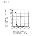
- FIG. 5 is a graph showing the relationship between the water partial pressure in forming the interface layer 14a and the crystallization ratio.
- the axis of abscissas indicates the water partial pressure in forming the interface layer 14a, while the axis of ordinates indicates the crystallization ratio.
- the crystallization ratio is defined by (the area where a crystal lattice image can be confirmed) / (the total area) observed by a transmission electron microscope.
- the bulk layer 14b of every sample evaluated in FIG. 4 has a crystallization ratio of not less than 98%, which is higher than the crystallization ratio of the interface layer 14a.
- the reason for this is that, since the photovoltaic element is required to provide a high output, the ITO film 14 needs to achieve both low resistance and high transmittance, and therefore a high crystallization ratio is essential.
- Table 1 shows the relationship between the crystallization ratio of the ITO single-layer film and the normalized output of the photovoltaic element in the ITO single-layer structure. Crystallization ratio (%) 100 95 88 2 Normalized output 1.00 0.98 0.72 0.64
- a normalized output is an output normalized by an output obtained when the crystallization ratio is 100%. As shown in Table 1, when the crystallization ratio is 95% or more, it is possible to keep high level normalized outputs, but, when the crystallization ratio is lower than 95%, the output of the photovoltaic element decreases largely due to an increase in resistance and an increase in absorption loss.
- FIG. 6 is a graph showing the Na concentration in the photovoltaic element.
- the axis of abscissas indicates the Na concentration, while the axis of ordinates indicates the thickness from the interface between the semiconductor layer 13 and the ITO film 14.
- the Na concentration in the bulk layer 14b of the ITO film 14 is almost constant, but the Na concentration decreases abruptly in the interface layer 14a which was treated by adjusting the water partial pressure appropriately, and it was confirmed that alkaline ions are effectively blocked by the interface layer 14a of the ITO film 14.
- the photovoltaic element of the present invention is characterized in that, in the transparent conductive film (ITO film 14), the interface region with a thickness of not more than 20 ⁇ on a side of the transparent conductive film adjacent to the semiconductor layer 13, which is a light incident side, has a relatively lower crystallinity than the bulk region formed on the interface region and includes an amorphous structure.
- a photovoltaic device such as a solar cell and an optical sensor, which has both improved photoelectric conversion characteristic and alkali resistance.
- the transparent conductive film is made of a single material (ITO), in other words, the alkali diffusion prevention region and other region are made of the same material (ITO), it is possible to make these two regions by using different materials.
- FIG. 7 and FIG. 8 are the perspective view and schematic cross sectional view showing such an example of photovoltaic element of the present invention.
- the same parts as in FIG. 1 and FIG. 2 are designated with the same numbers, and the explanation of these parts is omitted.
- a transparent conductive film 24 of this example is composed of an alkali diffusion prevention film 24a on the semiconductor layer 13 side and an ITO film 24b on the collecting electrode 15 side.
- the alkali diffusion prevention film 24a has the function of reducing the diffusion of alkaline ions, and specifically is made of a film of amorphous SiO, SiN and SiON, a transparent conductive film including at least one of SiO, SiN and SiON, or a transparent metal film such as Ag, Al and Au with a thickness ranging from several ⁇ to 100 ⁇ .
- the layer adjacent to the ITO film 14 or the transparent conductive film 24 is the p-type amorphous silicon hydride layer 13c
- the ITO film 14 or the transparent conductive film 24 explained in the above examples is also applicable to an amorphous solar cell in which light is incident from the opposite side of the silicon wafer 13a, a microcrystalline solar cell, and a hybrid structure composed of an amorphous solar cell and a microcrystalline solar cell.
- the transparent conductive film comprises the alkali diffusion prevention region, it is possible to reduce the diffusion of alkaline ions through the grain boundaries as a path, and achieve both high efficiency and environment resistance reliability required for the photovoltaic element.
Landscapes
- Photovoltaic Devices (AREA)
- Light Receiving Elements (AREA)
Abstract
Description
- The present invention relates to a photovoltaic element for use in a solar cell, an optical sensor, etc. having a structure comprising a transparent conductive film deposited on a semiconductor layer, like a pin junction, and also relates to a method for manufacturing the photovoltaic element.
- In recent years, the introduction of a photovoltaic power generation system that is installed on the roof of a house has been promoted rapidly. A solar cell for use in the photovoltaic power generation system utilizes, for example, a photovoltaic element which is manufactured by depositing i-type and p-type amorphous or microcrystalline semiconductor layers and a transparent conductive film made of a material such as an indium tin oxide (ITO) and zinc oxide (ZnO) successively on an n-type crystalline silicon wafer and then forming a collecting electrode on the transparent conductive film.
- Since a solar cell using such a photovoltaic element is generally mounted outdoors, it needs to have high environment resistance reliability. Hence, conventionally, when a photovoltaic element is incorporated as a product into a module, a cover glass is often used for the purpose of protecting the photovoltaic element, and thereby ensuring environmental resistance of the module.
- However, since, in general, inexpensive white plate glass is used as the cover glass, alkaline ions such as Na, Li and K contained in the white plate glass are sometimes diffused into the amorphous or microcrystalline semiconductor layers through the transparent conductive film under conditions such as a high humidity condition and exert a vicious influence. For example, when alkaline ions are diffused into the amorphous or microcrystalline semiconductor layers, this diffusion causes a diffusion potential change and may cause the problem of deterioration in the characteristics of the photovoltaic element.
- It is therefore desirable that the photovoltaic element itself should have excellent environment resistance, particularly, good resistance to alkaline ions, and there has been a demand for an improved transparent conductive film. Moreover, in order to achieve high efficiency, the transparent conductive film of the photovoltaic element is required to have high light transmittance and low electrical resistance. In general, in order to realize high light transmittance and low electrical resistance, it is necessary to improve the crystallinity of the transparent conductive film. However, when ITO and ZnO which are polycrystalline substances are used, the crystal grains become larger, and accordingly the influence of the crystal grain boundaries increases. Thus, there are possibilities of promotion of diffusion of alkaline ions through the grain boundaries as a path and a decrease in the environment resistance reliability.
- The present invention has been made with the aim of solving the above problems, and it is an object of the present invention to provide a photovoltaic element capable of increasing the environment resistance reliability without decreasing the efficiency of the photovoltaic element and also to provide a method for manufacturing the photovoltaic element.
- A photovoltaic element of the present invention comprises an alkali diffusion prevention region within a transparent conductive film. Hence, diffusion of alkaline ions into a semiconductor layer through the transparent conductive film is prevented by this alkali diffusion prevention region, and the environmental resistance reliability increases.
- This alkali diffusion prevention region is provided on a side adjacent to the semiconductor layer, and the crystallinity in this region is lower than that in other region of the transparent conductive film. In the alkali diffusion prevention region with low crystallinity, the influence of the crystal grain boundaries is smaller, and the diffusion of alkaline ions through the boundaries as a path is reduced. In the other region with high crystallinity, since it is possible to realize high light transmittance and low electrical resistance, the efficiency of the photovoltaic element does not decrease. It is thus possible to achieve both high efficiency and high environmental resistance reliability required for the photovoltaic element.
- The alkali diffusion prevention region is in an amorphous state, for example. As the alkali diffusion prevention region, it is possible to use a film containing, for example, silicon oxide, silicon nitride or a mixture thereof, or a transparent metal film with a thickness ranging from several Å to 100 Å.
- In the case where the alkali diffusion prevention region and the other region are made of the same material (for example, ITO) of different crystallinity, they can be fabricated easily. In this case, a preferred crystallization ratio in the alkali diffusion prevention region is 0% to 90%, and more particularly 0% to 10%. Thus, in the alkali diffusion prevention region, the influence of the crystal grain boundaries is smaller, and the diffusion of alkaline ions through the boundaries as a path is reduced. Besides, the thickness of the alkali diffusion prevention region is preferably not more than 20 Å. Hence, in the alkali diffusion prevention region, the influence of the crystal grain boundaries is smaller, and the diffusion of alkaline ions through the boundaries as a path is reduced. In the other region, since high light transmittance and low electrical resistance can be realized, it is possible to prevent a decrease in the energy conversion efficiency of the photovoltaic element.
- As the semiconductor layer, any one of a-Si:H, a-SiC:H, a-SiGe:H, µc-Si:H, µc-SiC:H, and µc-SiGe:H is used. It is therefore possible to limit deposition of crystals in the interface region of the transparent conductive film with the semiconductor layer, and easily form the transparent conductive film in an amorphous state.
- In a method for manufacturing a photovoltaic element of the present invention, when layering a transparent conductive film, a first layer is formed at a first water partial pressure and a second layer is formed at a second water partial pressure. At this time, by setting the first water partial pressure to be higher than the second water partial pressure, the crystallization ratio of the first layer that is a layer on a side adjacent to the semiconductor layer can be made lower, and therefore it is possible to increase the alkaline ion resistance in the first layer.
- Moreover, by setting the first water partial pressure not to be lower than 5×10⁻⁴ Pa but not to be higher than 5×10⁻³ Pa, it is possible to increase the alkaline ion resistance without decreasing the energy conversion efficiency in the first layer. Furthermore, a heat treatment is performed after forming the first layer. It is thus possible to crystallize a part while holding the amorphous state in the first layer, and increase the energy conversion efficiency without decreasing the alkaline ion resistance.
- The above and further objects and features of the invention will more fully be apparent from the following detailed description with accompanying drawings.
-
- FIG. 1 is a perspective view showing one example of photovoltaic element of the present invention;
- FIG. 2 is a schematic cross sectional view showing one example of photovoltaic element of the present invention;
- FIG. 3 is a graph showing the relationship between the water partial pressure in forming an interface layer and the normalized initial efficiency;
- FIG. 4 is a graph showing the relationship between the water partial pressure in forming the interface layer and the alkali resistance;
- FIG. 5 is a graph showing the relationship between the water partial pressure in forming the interface layer and the crystallization ratio;
- FIG. 6 is a graph showing the Na concentration in the photovoltaic element;
- FIG. 7 is a perspective view showing another example of photovoltaic element of the present invention; and
- FIG. 8 is a schematic cross sectional view showing another example of photovoltaic element of the present invention.
-
- The following description will explain the present invention in detail, based on the drawings illustrating some embodiments thereof.
- FIG. 1 and FIG. 2 are the perspective view and schematic cross sectional view showing one example of photovoltaic element of the present invention. In these figures, 13 is a semiconductor layer comprising a pin junction. The
semiconductor layer 13 is constructed by forming an i-type amorphous silicon hydride layer13b and a p-type amorphoussilicon hydride layer 13c on the front surface of an n-type silicon wafer (thickness: 300 µm) 13a. - A Sn-doped indium tin oxide film 14 (hereinafter referred to as the "ITO
film 14"), that is a transparent conductive film, is deposited on the front surface of this semiconductor layer 13 (p-type amorphoussilicon hydride layer 13c). By controlling the water partial pressure when forming theITO film 14 as described later, it is possible to control the crystallinity of an interface layer 14a in the vicinity of the boundary with thesemiconductor layer 13 and in abulk layer 14b on the interface layer 14a. This interface layer 14a functions as an alkali diffusion prevention region for preventing alkali diffusion. In the present invention, the interface layer 14a has a low crystallinity, while theother bulk layer 14b has a high crystallinity. - Formed on the ITO
film 14 is a comb-like collectingelectrode 15 made of a silver paste obtained by kneading a silver fine powder into an epoxy resin. Furthermore, on the back surface of the semiconductor layer 13 (silicon wafer 13a), aback electrode 12 is formed by vapor-depositing a metal film such as Ag and Al. - A photovoltaic device such as a solar cell and an optical sensor incorporates a photovoltaic element including the above-mentioned
back electrode 12,semiconductor layer 13,ITO film 14 and collectingelectrode 15 as a module, and comprises a transparent resin film (not shown) on theITO film 14 and collectingelectrode 15 and further a cover glass (not shown) containing alkaline ions such as Na, Li and K on the resin film so as to protect the photovoltaic element over a long period of time. - The following description will explain a method for manufacturing the photovoltaic element shown in FIG. 1 and FIG. 2.
- After removing impurities from the n-type (100) silicon wafer 13a with a relative resistance of about 1 Ω·cm and a thickness of 300 µm by normal washing, the i-type amorphous
silicon hydride layer 13b and the p-type amorphoussilicon hydride layer 13c are deposited in about 5 nm each by a known RF plasma CVD technique so as to form a pin junction. The formation temperature when depositing the i-type amorphoussilicon hydride layer 13b and the p-type amorphoussilicon hydride layer 13c is 100°C to 300°C, the reaction pressure is 5 Pa to 100 Pa, and the RF power is 1 mW/cm2 to 500 mW/cm2. - As a p-type dopant used when forming the p-type amorphous
silicon hydride layer 13c, any one of B, Al, Ga and In, which aregroup 13 elements, is used. By mixing a compound gas containing at least one of these elements into a source gas such as SiH4, it is possible to control the layer to p-type. Besides, in order to obtain the n-type silicon wafer 13a, a compound gas containing at least one of P, N, As and Sb, which aregroup 15 elements, is used. - Each of the i-type amorphous
silicon hydride layer 13b and the p-type amorphoussilicon hydride layer 13c can be formed by using known techniques such as a vapor deposition technique, a sputtering technique, a microwave plasma CVD technique, an ECR technique, a thermal CVD technique, and an LPCVD technique, instead of the RF plasma CVD technique. The semiconductor that forms thesemiconductor layer 13 may be a crystalline semiconductor, an amorphous semiconductor containing at least one of hydrogen and fluorine, or microcrystalline of any one of Si, SiGe, SiGeC, SiC, SiN, SiGeN, SiSn, SiSnN, SiSnO, SiO, Ge, GeC and GeN. - Next, the
ITO film 14 as a transparent conductive film is formed on the front surface of the p-type amorphoussilicon hydride layer 13c. It was found as a result of research by the present inventor et al. that theITO film 14 having the characteristics of the present invention is obtainable by the following technique. - A sintered body of an In2O3 powder mixed with 5 wt% of SnO2 powder is mounted as a target on the cathode. Although the amount of Sn contained in the
ITO film 14 can be changed by changing the amount of SnO2 to be mixed, the amount of Sn, based on In, is preferably 1 at% to 10 at%, and more preferably 3 at% to 7 at%. The sintered density of the target is preferably 90% or more. Note that, instead of SnO2, it is possible to use at least one of Zn, As, Ca, Cu, F, Ge, Mg, S, Si and Te as the dopant. - Then, after placing a sample to be parallel to and face the cathode, a chamber is evacuated. The temperature of the sample is kept at 25°C to 150°C using a heater, the pressure is kept at 0.4 Pa to 1.3 Pa by a flow of a mixed gas of Ar and O2, and 1 kW DC power is supplied to the cathode so as to start discharging. The film deposition rate when the sample is stationary against the cathode is about 67 nm/min. Instead of Ar, it is possible to use an inert gas such as He, Ne, Kr and Xe, or a mixed gas thereof. It is also possible to perform gas discharge by pulse modulation DC discharge, RF, VHF, or microwave discharge.
- Next, the comb-
like collecting electrode 15 is formed on theITO film 14. After forming the collectingelectrode 15 in a height of 10 µm to 30 µm and a width of 100 µm to 500 µm by screen printing using a silver paste obtained by kneading a silver fine powder into an epoxy resin, it is sintered and hardened for 80 minutes at 200°C so as to form a shape having a plurality of mutually parallel branch parts. Then, theback electrode 12 is formed by vapor-depositing a metal film such as Ag and Al on the back surface of thesemiconductor layer 13. - The following description will explain the results of the characteristic evaluation tests performed by the present inventor et al. on the
ITO film 14. The characteristic evaluation tests were performed so as to evaluate the energy conversion efficiency and the resistance to sodium ions (alkali resistance). Here, the evaluation of the resistance to sodium ions was performed by applying 0.1 g of NaHCO3 aqueous solution to theITO film 14, leaving it for 3 hours at 200°C, and then measuring the output of the photovoltaic element (Pmax after Na test). - FIG. 3 is a graph showing the relationship between the water partial pressure in forming the interface layer 14a and the normalized initial efficiency. The axis of abscissas indicates the water partial pressure in forming the interface layer 14a, while the axis of ordinates indicates the value of output of the photovoltaic element when the interface layer 14a was formed by changing the water partial pressure. Note that the axis of ordinates is normalized by the value of output of the photovoltaic element when an ITO single-layer film was formed as the transparent conductive film at a water partial pressure of 1×10⁻³ Pa.
- Prior to the evaluation of the characteristics of the interface layer 14a, first, with the use an ITO target doped with 5 at% SnO2, the interface layer 14a was deposited in a thickness of 20 Å on the surface of the
semiconductor layer 13 at a water partial pressure of 5×10⁻² Pa to 1×10⁻⁴ Pa, a pressure of 0.5 Pa, a DC power of 1 kW and a substrate temperature of 200°C under the conditions that the Ar flow rate was 200 sccm and the oxygen flow rate was 12 sccm, and then thebulk layer 14b was deposited in a thickness of 980 Å on the interface layer 14a at a water partial pressure of 1×10⁻⁴ Pa, thereby forming the photovoltaic element. Besides, the photovoltaic element which was used to normalize the output is an ITO single-layer film (with a thickness of 1000 Å) formed at a constant water partial pressure (1×10⁻³ Pa). - As shown in FIG. 3, when the water partial pressure in forming the interface layer 14a was 1×10⁻³ Pa or less, the output was equal to or more than that obtained when the ITO single-layer film was formed. However, it was confirmed that, when the water partial pressure in forming the interface layer 14a was 2.5×10⁻³ Pa or more, the output decreased due to a decrease in the curve factor and open-circuit voltage.
- FIG. 4 is a graph showing the relationship between the water partial pressure in forming the interface layer 14a and the alkali resistance. The axis of abscissas indicates the water partial pressure in forming the interface layer 14a, while the axis of ordinates indicates the value obtaining by normalizing Pmax after Na test by the initial output before applying the NaHCO3 aqueous solution (Pmax before Na test).
- As shown in FIG. 4, when the water partial pressure in forming the interface layer 14a was 1×10⁻³ Pa or more, a decrease in the output was not seen in the alkali resistance test. However, it was found that the alkali resistance decreased at a water partial pressure lower than 1×10⁻³ Pa. Moreover, the crystallinity was evaluated by X-ray diffraction. In the case of the interface layer 14a formed at a water partial pressure of 1×10⁻³ Pa or more, even when a heat treatment was applied in forming the collecting
electrode 15, a random diffraction distribution representing amorphous was observed in the interface layer 14a. In addition, it was confirmed that the amorphous component increased with an increase in the water partial pressure in forming the interface layer 14a. - The above results indicate that, when the interface layer 14a of the
ITO film 14 was formed on the front surface of the p-type amorphoussilicon hydride layer 13c at a high water partial pressure of not lower than 1×10⁻³ Pa, the interface layer 14a containing the amorphous component was formed, and a part of the amorphous component remained, although the crystallinity was improved by the heat treatment performed thereafter in forming the collectingelectrode 15. It was also confirmed by observation using a transmission electron microscope that a particularly large amount of amorphous component was present in a region of the interface layer 14a closest to the p-type amorphoussilicon hydride layer 13c. - It was also found from FIG. 3 and FIG. 4 that, in order to achieve both improved initial output and alkali resistance, there is an optimum condition for the water partial pressure in forming the interface region with a thickness of not more than 20 Å of the
ITO film 14 on a side adjacent to thesemiconductor layer 13, and, in this embodiment, the water partial pressure is 1×10⁻³ Pa. - FIG. 5 is a graph showing the relationship between the water partial pressure in forming the interface layer 14a and the crystallization ratio. In FIG. 5, the axis of abscissas indicates the water partial pressure in forming the interface layer 14a, while the axis of ordinates indicates the crystallization ratio. Here, the crystallization ratio is defined by (the area where a crystal lattice image can be confirmed) / (the total area) observed by a transmission electron microscope.
- As shown in FIG. 5, the higher the water partial pressure in forming the interface layer 14a, the lower the crystallization ratio. In other words, in view of FIG. 5 together with FIG. 4, it was confirmed that the alkali resistance can be improved significantly with a crystallization ratio of not higher than 10%.
- Note that the
bulk layer 14b of every sample evaluated in FIG. 4 has a crystallization ratio of not less than 98%, which is higher than the crystallization ratio of the interface layer 14a. The reason for this is that, since the photovoltaic element is required to provide a high output, theITO film 14 needs to achieve both low resistance and high transmittance, and therefore a high crystallization ratio is essential. - Here, Table 1 shows the relationship between the crystallization ratio of the ITO single-layer film and the normalized output of the photovoltaic element in the ITO single-layer structure.
Crystallization ratio (%) 100 95 88 2 Normalized output 1.00 0.98 0.72 0.64 - A normalized output is an output normalized by an output obtained when the crystallization ratio is 100%. As shown in Table 1, when the crystallization ratio is 95% or more, it is possible to keep high level normalized outputs, but, when the crystallization ratio is lower than 95%, the output of the photovoltaic element decreases largely due to an increase in resistance and an increase in absorption loss.
- FIG. 6 is a graph showing the Na concentration in the photovoltaic element. The axis of abscissas indicates the Na concentration, while the axis of ordinates indicates the thickness from the interface between the
semiconductor layer 13 and theITO film 14. As shown in FIG. 6, the Na concentration in thebulk layer 14b of theITO film 14 is almost constant, but the Na concentration decreases abruptly in the interface layer 14a which was treated by adjusting the water partial pressure appropriately, and it was confirmed that alkaline ions are effectively blocked by the interface layer 14a of theITO film 14. - As described above, the photovoltaic element of the present invention is characterized in that, in the transparent conductive film (ITO film 14), the interface region with a thickness of not more than 20 Å on a side of the transparent conductive film adjacent to the
semiconductor layer 13, which is a light incident side, has a relatively lower crystallinity than the bulk region formed on the interface region and includes an amorphous structure. Moreover, with the use of such a photovoltaic element, it is possible to realize a photovoltaic device, such as a solar cell and an optical sensor, which has both improved photoelectric conversion characteristic and alkali resistance. - Note that although the above-described embodiment illustrates an example in which the transparent conductive film is made of a single material (ITO), in other words, the alkali diffusion prevention region and other region are made of the same material (ITO), it is possible to make these two regions by using different materials.
- FIG. 7 and FIG. 8 are the perspective view and schematic cross sectional view showing such an example of photovoltaic element of the present invention. In FIG. 7 and FIG. 8, the same parts as in FIG. 1 and FIG. 2 are designated with the same numbers, and the explanation of these parts is omitted.
- A transparent
conductive film 24 of this example is composed of an alkali diffusion prevention film 24a on thesemiconductor layer 13 side and an ITO film 24b on the collectingelectrode 15 side. Like the above-mentioned interface layer 14a, the alkali diffusion prevention film 24a has the function of reducing the diffusion of alkaline ions, and specifically is made of a film of amorphous SiO, SiN and SiON, a transparent conductive film including at least one of SiO, SiN and SiON, or a transparent metal film such as Ag, Al and Au with a thickness ranging from several Å to 100 Å. - With such a structure, it is also possible to realize the alkali ion diffusion reducing function of the alkali diffusion prevention film 24a, and the function of the ITO film 24b to achieve both high light transmittance and low electrical resistance.
- Note that, in the above-illustrated examples, although the layer adjacent to the
ITO film 14 or the transparentconductive film 24 is the p-type amorphoussilicon hydride layer 13c, it is also possible to implement a mode in which an i-type amorphous silicon hydride layer and an n-type amorphous silicon hydride layer are successively deposited on a p-type microcrystalline silicon wafer, and then theITO film 14 as a transparent conductive film or the transparentconductive film 24 is formed on the front surface of the n-type amorphous silicon hydride layer. - Of course, the
ITO film 14 or the transparentconductive film 24 explained in the above examples is also applicable to an amorphous solar cell in which light is incident from the opposite side of the silicon wafer 13a, a microcrystalline solar cell, and a hybrid structure composed of an amorphous solar cell and a microcrystalline solar cell. - As described in detail above, in the photovoltaic element of the present invention, since the transparent conductive film comprises the alkali diffusion prevention region, it is possible to reduce the diffusion of alkaline ions through the grain boundaries as a path, and achieve both high efficiency and environment resistance reliability required for the photovoltaic element.
Claims (14)
- A photovoltaic element comprising a semiconductor layer (13) and a transparent conductive film (14, 24), characterized in that said transparent conductive film (14, 24) has an alkali diffusion prevention region (14a, 24a).
- The photovoltaic element of claim 1,
wherein said transparent conductive film (14, 24) has the alkali diffusion prevention region (14a, 24a) on a side adjacent to said semiconductor layer (13). - The photovoltaic element of claim 1 or 2,
wherein the alkali diffusion prevention region (14a, 24a) has a lower crystallinity than other region (14b, 24b) of said transparent conductive film (14, 24). - The photovoltaic element of any one of claims 1 through 3,
wherein the alkali diffusion prevention region (14a, 24a) is amorphous. - The photovoltaic element of any one of claims 1 through 4,
wherein the alkali diffusion prevention region (24a) includes silicon oxide, silicon nitride or a mixture thereof. - The photovoltaic element of claim 1 or 2,
wherein the alkali diffusion prevention region (24a) includes a transparent metal film. - The photovoltaic element of claim 6,
wherein the metal film has a thickness ranging from several Å to 100 Å. - The photovoltaic element of claim 1 or 2,
wherein the alkali diffusion prevention region (14a) and other region (14b) of said transparent conductive film (14) are made of same material, and the alkali diffusion prevention region (14a) has a lower crystallinity compared to the other region (14b). - The photovoltaic element of claim 8,
wherein a crystallization ratio in the alkali diffusion prevention region (14a) is 0% to 90%, and preferably 0% to 10%. - The photovoltaic element of claim 8 or 9,
wherein the alkali ion diffusion prevention region (14a) has a thickness of not more than 20 Å. - The photovoltaic element of any one of claims 1 through 10,
wherein said semiconductor layer (13) includes a material selected from the group consisting of a-Si:H, a-SiC:H, a-SiGe:H, µc-Si:H, µc-SiC:H, and µc-SiGe:H. - A method for manufacturing a photovoltaic element by layering a transparent conductive film (14) on a semiconductor layer (13), characterized by forming a first layer (14a) at a first water partial pressure and then forming a second layer (14b) at a second water partial pressure different from the first water partial pressure when layering the transparent conductive film (14) on the semiconductor layer (13).
- The method for manufacturing a photovoltaic element of claim 12,
wherein the first water partial pressure is not lower than 5×10⁻⁴ Pa but not higher than 5×10⁻³ Pa. - The method for manufacturing a photovoltaic element of claim 12 or 13,
wherein, after forming the first layer (14a), a heat treatment is performed on the first layer (14a).
Applications Claiming Priority (2)
| Application Number | Priority Date | Filing Date | Title |
|---|---|---|---|
| JP2002076977 | 2002-03-19 | ||
| JP2002076977A JP3679771B2 (en) | 2002-03-19 | 2002-03-19 | Photovoltaic device and method for manufacturing photovoltaic device |
Publications (2)
| Publication Number | Publication Date |
|---|---|
| EP1351317A2 true EP1351317A2 (en) | 2003-10-08 |
| EP1351317A3 EP1351317A3 (en) | 2010-12-15 |
Family
ID=28035478
Family Applications (1)
| Application Number | Title | Priority Date | Filing Date |
|---|---|---|---|
| EP03354025A Withdrawn EP1351317A3 (en) | 2002-03-19 | 2003-03-19 | Photovoltaic element and manufacturing method of the photovoltaic element |
Country Status (4)
| Country | Link |
|---|---|
| US (1) | US6849917B2 (en) |
| EP (1) | EP1351317A3 (en) |
| JP (1) | JP3679771B2 (en) |
| CN (1) | CN1233044C (en) |
Families Citing this family (19)
| Publication number | Priority date | Publication date | Assignee | Title |
|---|---|---|---|---|
| EP1555695B1 (en) * | 2004-01-13 | 2011-05-04 | Sanyo Electric Co., Ltd. | Photovoltaic device |
| JP2005203659A (en) * | 2004-01-19 | 2005-07-28 | Sony Corp | Photoelectric conversion material and method for producing the same, photoelectric conversion element and method for producing the same, electronic device and method for producing the same |
| JP4821033B2 (en) * | 2006-01-25 | 2011-11-24 | 石塚硝子株式会社 | Concentrating solar power generation unit and its columnar optical glass member |
| KR20090007063A (en) * | 2007-07-13 | 2009-01-16 | 삼성에스디아이 주식회사 | Solar cell and manufacturing method thereof |
| US7960644B2 (en) * | 2007-11-09 | 2011-06-14 | Sunpreme, Ltd. | Low-cost multi-junction solar cells and methods for their production |
| JP5059628B2 (en) * | 2008-01-10 | 2012-10-24 | 株式会社日立製作所 | Semiconductor device |
| US8796066B2 (en) * | 2008-11-07 | 2014-08-05 | Sunpreme, Inc. | Low-cost solar cells and methods for fabricating low cost substrates for solar cells |
| US7951640B2 (en) * | 2008-11-07 | 2011-05-31 | Sunpreme, Ltd. | Low-cost multi-junction solar cells and methods for their production |
| US8742531B2 (en) * | 2008-12-08 | 2014-06-03 | Arizona Board Of Regents, Acting For And On Behalf Of Arizona State University | Electrical devices including dendritic metal electrodes |
| CN101924145B (en) * | 2009-06-12 | 2013-01-23 | 大同大学 | Photoelectric conversion device and manufacturing method thereof |
| JPWO2012020682A1 (en) * | 2010-08-09 | 2013-10-28 | 株式会社カネカ | Crystalline silicon solar cell |
| CN102097541B (en) * | 2010-11-02 | 2012-12-12 | 南开大学 | Method for enhancing efficiency of industrial single-chamber deposited amorphous silicon-based solar cell |
| CN103430319B (en) * | 2011-03-31 | 2016-01-20 | 京瓷株式会社 | Solar cell device and solar module |
| WO2013061637A1 (en) * | 2011-10-27 | 2013-05-02 | 三菱電機株式会社 | Photoelectric conversion device and method for manufacturing same, and photoelectric conversion module |
| JP6139261B2 (en) * | 2013-05-17 | 2017-05-31 | 株式会社カネカ | SOLAR CELL, MANUFACTURING METHOD THEREOF, AND SOLAR CELL MODULE |
| JP6626482B2 (en) * | 2017-08-10 | 2019-12-25 | 株式会社東芝 | Semiconductor device and method of manufacturing the same |
| CN108321239A (en) * | 2017-12-21 | 2018-07-24 | 君泰创新(北京)科技有限公司 | A kind of solar energy hetero-junction solar cell and preparation method thereof |
| US12426518B2 (en) * | 2019-12-17 | 2025-09-23 | International Business Machines Corporation | Conductive oxide diffusion barrier for laser crystallization |
| US12532551B2 (en) | 2021-12-10 | 2026-01-20 | Boe Technology Group Co., Ltd. | Visible light communication device, display substrate, display device and manufacturing method of the display substrate |
Family Cites Families (9)
| Publication number | Priority date | Publication date | Assignee | Title |
|---|---|---|---|---|
| JPS6089573A (en) * | 1983-10-20 | 1985-05-20 | Ricoh Co Ltd | Transparent conductive film |
| JPH0614555B2 (en) * | 1986-03-14 | 1994-02-23 | 日本板硝子株式会社 | Transparent conductive film |
| JP3101962B2 (en) * | 1993-09-30 | 2000-10-23 | 京セラ株式会社 | Semiconductor element manufacturing method |
| DE4442824C1 (en) * | 1994-12-01 | 1996-01-25 | Siemens Ag | Solar cell having higher degree of activity |
| AU6420398A (en) * | 1997-03-21 | 1998-10-20 | Sanyo Electric Co., Ltd. | Photovoltaic element and method for manufacture thereof |
| EP1063317B1 (en) * | 1998-03-05 | 2003-07-30 | Asahi Glass Company Ltd. | Sputtering target, transparent conductive film, and method for producing the same |
| JP3247876B2 (en) * | 1999-03-09 | 2002-01-21 | 日本板硝子株式会社 | Glass substrate with transparent conductive film |
| JP2002025350A (en) * | 2000-07-11 | 2002-01-25 | Sanyo Electric Co Ltd | Substrate with transparent conductive film, method of manufacturing the same, etching method using the same, and photovoltaic device |
| JP2002299657A (en) * | 2001-03-30 | 2002-10-11 | Sanyo Electric Co Ltd | Photovoltaic module |
-
2002
- 2002-03-19 JP JP2002076977A patent/JP3679771B2/en not_active Expired - Lifetime
-
2003
- 2003-03-17 US US10/388,449 patent/US6849917B2/en not_active Expired - Lifetime
- 2003-03-19 CN CNB031204708A patent/CN1233044C/en not_active Expired - Lifetime
- 2003-03-19 EP EP03354025A patent/EP1351317A3/en not_active Withdrawn
Non-Patent Citations (1)
| Title |
|---|
| None |
Also Published As
| Publication number | Publication date |
|---|---|
| US6849917B2 (en) | 2005-02-01 |
| CN1445866A (en) | 2003-10-01 |
| EP1351317A3 (en) | 2010-12-15 |
| JP3679771B2 (en) | 2005-08-03 |
| JP2003273380A (en) | 2003-09-26 |
| US20030178630A1 (en) | 2003-09-25 |
| CN1233044C (en) | 2005-12-21 |
Similar Documents
| Publication | Publication Date | Title |
|---|---|---|
| US6849917B2 (en) | Photovoltaic element | |
| EP1786040B1 (en) | Photovoltaic element and photovoltaic device | |
| US6459034B2 (en) | Multi-junction solar cell | |
| US6388301B1 (en) | Silicon-based thin-film photoelectric device | |
| KR100237661B1 (en) | Back reflective layer, method of forming the same, and photovoltaic device using the back reflective layer and manufacturing method thereof | |
| JP2022128577A (en) | Solar cell, manufacturing method thereof, and solar cell module | |
| JP6096790B2 (en) | Conductive substrate for photovoltaic cells | |
| US8519435B2 (en) | Flexible photovoltaic cells having a polyimide material layer and method of producing same | |
| US20110259395A1 (en) | Single Junction CIGS/CIS Solar Module | |
| EP1320134A2 (en) | Photovoltaic device and manufacturing method thereof | |
| KR20090096637A (en) | Reactive sputter deposition method of transparent conductive film | |
| EP1553637A2 (en) | Photovoltaic device | |
| KR20100029414A (en) | Solar cell and method of fabricating the same | |
| US20040177878A1 (en) | Photovoltaic device and device having transparent conductive film | |
| US20170104110A1 (en) | Photovoltaic device containing an n-type dopant source | |
| EP1160877A2 (en) | Photovoltaic element and method of manufacturing the same | |
| EP2416370A1 (en) | Thin film solar fabrication process, deposition method for TCO layer, and solar cell precursor layer stack | |
| US20070169807A1 (en) | Photovoltaic Element, Photovoltaic Module Comprising Photovoltaic Element, and Method of Fabricating Photovoltaic Element | |
| JP2004260014A (en) | Multilayer type thin film photoelectric conversion device | |
| US20100307590A1 (en) | Photoelectric conversion device | |
| JP4219264B2 (en) | Photovoltaic device | |
| JPH01201968A (en) | Photoelectric conversion device | |
| JPH06151910A (en) | Photoelectromotive force element and generation system | |
| US20100147380A1 (en) | Hybrid Photovoltaic Cell Using Amorphous Silicon Germanium Absorbers and Wide Bandgap Dopant Layers | |
| JP4215694B2 (en) | Photoelectric conversion device and manufacturing method thereof |
Legal Events
| Date | Code | Title | Description |
|---|---|---|---|
| PUAI | Public reference made under article 153(3) epc to a published international application that has entered the european phase |
Free format text: ORIGINAL CODE: 0009012 |
|
| AK | Designated contracting states |
Kind code of ref document: A2 Designated state(s): AT BE BG CH CY CZ DE DK EE ES FI FR GB GR HU IE IT LI LU MC NL PT RO SE SI SK TR |
|
| AX | Request for extension of the european patent |
Extension state: AL LT LV MK |
|
| PUAL | Search report despatched |
Free format text: ORIGINAL CODE: 0009013 |
|
| AK | Designated contracting states |
Kind code of ref document: A3 Designated state(s): AT BE BG CH CY CZ DE DK EE ES FI FR GB GR HU IE IT LI LU MC NL PT RO SE SI SK TR |
|
| AX | Request for extension of the european patent |
Extension state: AL LT LV MK |
|
| 17P | Request for examination filed |
Effective date: 20110214 |
|
| AKX | Designation fees paid |
Designated state(s): DE FR IT |
|
| 17Q | First examination report despatched |
Effective date: 20120109 |
|
| STAA | Information on the status of an ep patent application or granted ep patent |
Free format text: STATUS: THE APPLICATION IS DEEMED TO BE WITHDRAWN |
|
| 18D | Application deemed to be withdrawn |
Effective date: 20131001 |