EP1351134A2 - Superpipelined arithmetic-logic unit with feedback - Google Patents
Superpipelined arithmetic-logic unit with feedback Download PDFInfo
- Publication number
- EP1351134A2 EP1351134A2 EP03006757A EP03006757A EP1351134A2 EP 1351134 A2 EP1351134 A2 EP 1351134A2 EP 03006757 A EP03006757 A EP 03006757A EP 03006757 A EP03006757 A EP 03006757A EP 1351134 A2 EP1351134 A2 EP 1351134A2
- Authority
- EP
- European Patent Office
- Prior art keywords
- data
- arithmetic
- latch circuit
- stage
- line
- Prior art date
- Legal status (The legal status is an assumption and is not a legal conclusion. Google has not performed a legal analysis and makes no representation as to the accuracy of the status listed.)
- Withdrawn
Links
Images










Classifications
-
- G—PHYSICS
- G06—COMPUTING OR CALCULATING; COUNTING
- G06F—ELECTRIC DIGITAL DATA PROCESSING
- G06F9/00—Arrangements for program control, e.g. control units
- G06F9/06—Arrangements for program control, e.g. control units using stored programs, i.e. using an internal store of processing equipment to receive or retain programs
- G06F9/30—Arrangements for executing machine instructions, e.g. instruction decode
- G06F9/38—Concurrent instruction execution, e.g. pipeline or look ahead
- G06F9/3867—Concurrent instruction execution, e.g. pipeline or look ahead using instruction pipelines
- G06F9/3875—Pipelining a single stage, e.g. superpipelining
-
- G—PHYSICS
- G06—COMPUTING OR CALCULATING; COUNTING
- G06F—ELECTRIC DIGITAL DATA PROCESSING
- G06F9/00—Arrangements for program control, e.g. control units
- G06F9/06—Arrangements for program control, e.g. control units using stored programs, i.e. using an internal store of processing equipment to receive or retain programs
- G06F9/30—Arrangements for executing machine instructions, e.g. instruction decode
- G06F9/30003—Arrangements for executing specific machine instructions
- G06F9/30007—Arrangements for executing specific machine instructions to perform operations on data operands
- G06F9/3001—Arithmetic instructions
- G06F9/30014—Arithmetic instructions with variable precision
-
- G—PHYSICS
- G06—COMPUTING OR CALCULATING; COUNTING
- G06F—ELECTRIC DIGITAL DATA PROCESSING
- G06F9/00—Arrangements for program control, e.g. control units
- G06F9/06—Arrangements for program control, e.g. control units using stored programs, i.e. using an internal store of processing equipment to receive or retain programs
- G06F9/30—Arrangements for executing machine instructions, e.g. instruction decode
- G06F9/30003—Arrangements for executing specific machine instructions
- G06F9/30007—Arrangements for executing specific machine instructions to perform operations on data operands
- G06F9/30036—Instructions to perform operations on packed data, e.g. vector, tile or matrix operations
-
- G—PHYSICS
- G06—COMPUTING OR CALCULATING; COUNTING
- G06F—ELECTRIC DIGITAL DATA PROCESSING
- G06F9/00—Arrangements for program control, e.g. control units
- G06F9/06—Arrangements for program control, e.g. control units using stored programs, i.e. using an internal store of processing equipment to receive or retain programs
- G06F9/30—Arrangements for executing machine instructions, e.g. instruction decode
- G06F9/38—Concurrent instruction execution, e.g. pipeline or look ahead
- G06F9/3885—Concurrent instruction execution, e.g. pipeline or look ahead using a plurality of independent parallel functional units
- G06F9/3893—Concurrent instruction execution, e.g. pipeline or look ahead using a plurality of independent parallel functional units controlled in tandem, e.g. multiplier-accumulator
Definitions
- the present invention relates to a serial operation pipeline suitable for an application requiring a discrete operation in which the amount to be operated expands extemporaneously and explosively, for example, an application requiring for expressing a frequently moving object by computer graphics, and structural elements thereof.
- the serial operation pipeline sequentially conducts different operations such as a command fetch operation, a command decode operation or a command execute operation at the same time, thereby increasing processing speed.
- the pipeline comprises computing units that deal with a small number of command groups, and the units are connected to each other in a cascade fashion.
- the combination of the plural computing units to be used is appropriately changed so as to realize various processing such as addition, subtraction and multiplication, a floating-point operation, comparison, Boolean algebra, or select (IF statement).
- Most of the conventional processors of this type are made up of a single device, and a plurality of operation pipelines are installed in parallel into the processor in accordance with an estimated amount of operation.
- a given function is fixedly allocated to each of individual computing units that structure the operation pipelines, which is so-called "one computing unit with one function".
- the pipeline using the one computing unit with one function is very suitable for, for example, the application that processes the data size of a fixed length by a short throughput.
- the one computing unit with one function for various purposes.
- a selector for connecting a path of data to be subjected to operation and an allocated function.
- the computing units or the operation pipelines are restrictively disposed in parallel within a single device.
- a control and a data path are required for preventing the cluster, respectively, thereby leading to the deterioration of an integration efficiency.
- a programmable data flow graph In order to cope with a variety of applications, it is proposed to structure a programmable data flow graph (DFG).
- the programmable DFG is relatively high in the occupied ratio of non-operation elements such as the selector with respect to the computing unit. There has been well known that the ratio becomes higher as the programmability of the operation is enhanced higher. Also, it is difficult to always execute all the functions of the programmable DFG because the functions are divided into sub-functions. In order to enhance the execution efficiency, the functions must be brought into function blocks the object of which are fixed to some degree, and become improper for the application that processes various types of data.
- the two-dimensional parallel means that the computing units are arranged in parallel and in cascade. That is, data flows are disposed in parallel due to deep pipelines. As an especial implement, there are rendering pipelines that are disposed in parallel. In making the two-dimensional parallel, only necessary functions are supplied within the pipelines, and the programmability is removed as much as possible, to thereby enhance the efficiency by the cascade connection of the exclusive computing units.
- the present invention has been made under the above circumstances, and therefore an object of the present invention is to realize various operations by one computing unit without increasing the costs.
- a serial operation pipeline in which a plurality of arithmetic-logic circuits which are controlled, independently, and operable together with another arithmetic-logic circuit are connected in a cascade fashion.
- all or a part of the plurality of arithmetic-logic circuits include a first line for outputting data from an upstream stage to a downstream stage, a second line for feeding back the data from the downstream stage to the upstream stage, and a latch circuit that latches data on the respective lines.
- the first line comprises a forward line for outputting the data received from the upstream stage or an operation result based on the data received from the upstream stage to the downstream stage
- the second line comprises a backward line for outputting the data received from the downstream stage or an operation result based on the data received from the upstream stage to the upstream stage.
- Each of the plural arithmetic-logic circuits includes a decoder that executes a process including an operation corresponding to the contents of an externally supplied instruction, and outputs an execution result toward a desired line.
- the latch circuit includes a first data latch circuit that latches a first output data which is outputted to the downstream stage, a second data latch circuit that latches a second output data which is outputted to the downstream stage, a carry latch circuit that latches a carry resulting from the operation made by the decoder for the operation of a succeeding figure, and a shift latch circuit that delays one of the first output data and the second output data for a given period of time and can make reference to the other data.
- the latch circuit may further include a reverse latch circuit that latches reverse data which is fed back to the upstream stage, and a control latch circuit that latches control data which determines an output timing of the data latched in the first and second data latch circuits and the reverse latch circuit.
- the data which is processed by the decoder is set to data of a unit processing size, for example, data of the shortest bit length or the equivalent bit length which can be processed by one clock that determines the operation timing of the plural arithmetic-logic circuits.
- an arithmetic device including a switch connection means that switches and connects data input/output lines of plural systems, a plurality of serial operation pipelines which are connected in parallel with the switch connection means, and an instruction receive mechanism that receives an externally supplied instruction for the plural serial operation pipelines.
- each of the plural serial operation pipelines comprises a serial operation pipeline in which a plurality of arithmetic-logic circuits which are operable together with another arithmetic-logic circuit are connected in a cascade fashion, and each of the plural arithmetic-logic circuits includes a forward line for outputting data received from the upstream stage or an operation result based on the data received from the upstream stage to the downstream stage, a backward line for feeding back the data received from the downstream stage or an operation result based on the data received from the upstream stage to the upstream stage, a decoder that executes a process corresponding to the inputted instruction and outputs an execution result to a desired line, and a latch circuit for synchronizing with the data output on each of the lines with respect to another arithmetic-logic circuit.
- the arithmetic device includes a controller, an instruction array which is the group of m x n instructions and held in the controller, and the controller outputs the instruction array toward the plural arithmetic-logic circuits m times for each of columns, and subtracts the executed instructions one by one for each of the stages when the pipelines are shifted to the downstream n times for each of the stages.
- an arithmetic procedure for executing the arithmetic operation by one path is determined.
- each latch circuit in the plural arithmetic-logic circuits includes a first data latch circuit that latches a first output data which is outputted to the downstream stage, a second data latch circuit that latches a second output data which is outputted to the downstream stage, a reverse latch circuit that latches data which is outputted to the upstream stage, a carry latch circuit that latches a carry resulting from the operation for the operation of a succeeding figure, a shift latch circuit that delays one of the first output data and the second output data for a given period of time and can make reference to the other data, and a control latch circuit that latches control data for controlling the operation of the data latched in the first and second data latch circuits and the reverse latch circuit.
- the data on the forward line and the data on the backward line in the respective decoders of the plural arithmetic-logic circuits are set as data of a unit processing size.
- the switch connection means, the plurality of serial operation pipelines and the instruction receive mechanism are installed in one semiconductor device, and a control signal of the switch connection means and the instruction array are inputted to the arithmetic device in accordance with the intended purposed, thereby being capable of providing the general-purpose property.
- an operation method using a serial operation pipeline comprises the steps of: structuring a serial operation pipeline by connecting in a cascade fashion a plurality of arithmetic-logic circuits including one or plural first lines for outputting data to a downstream stage, and a second line for feeding back the data to an upstream stage, which conduct serial operation and can select a line to which data representative of an operation result is outputted, independently; outputting an instruction array which is a group of n x m instructions, which reflect a procedure of simultaneous execution through one path by the plurality of arithmetic-logic circuits, toward the plurality of arithmetic-logic circuits m times for each of columns by an external controller which is connected to the serial operation pipeline, individually; and conducting such a control as to decrease the executed instructions by one for each of stages when the pipeline is shifted to the downstream stage n times for each of the stages.
- a serial computing unit conducts, for example, a serial operation of about 1 to 3 bits.
- the throughput of the serial computing unit reduces to 1/(data width) (in case of a one-bit serial operation) as compared with a parallel computing unit that conducts multiple-bits operation of about 16 bits, however a computing unit area is reduced along with the reduction of the throughput. Therefore, the more the parallel degree of the pipelines increases, the more the throughput reduces, as a result, the manufacture costs is not substantially different between the serial computing unit and the parallel computing unit.
- a 16-bit computing unit structured in such a manner that two 16-bit registers are disposed in parallel, their outputs are added by one 16-bit adder, and an addition result is stored in one 16-bit register as shown in Fig. 1A is substantially identical in the costs with 32 1-bit registers.
- the 32 1-bit registers are disposed in parallel, and 16 1-bit adders are disposed for adding the outputs of the respective two 1-bit registers together, and 16 1-bit registers are disposed for storing the outputs of the respective adders together as shown in Fig. 1B.
- the latter is advantageous in that the processing rate can be increased to the extent that the respective stages of the pipes are shortened.
- SALC serial arithmetic-logic circuits
- an SALC1 includes data input terminals D1i and D2i of two systems, data output terminals D1o and D2o of two systems, a reverse data input terminal Ri and a reverse data output terminal Ro of one system.
- the SALC1 is formed with a forward line for outputting data of the two systems from an upstream stage (a left side in the figure) to a downstream stage (a right side in the figure), and a backward line for feeding back the data from the downstream stage to the upstream stage.
- the output data is latched in a data latch circuit 11
- the reference data is latched in a reference latch circuit 12
- the reverse data is latched in a reverse latch circuit 13.
- the SALC 1 includes a decoder 10 that decodes the contents of an instruction which is inputted from an instruction input terminal CON, executes a process corresponding to the decode result, and selects a line that outputs an execution result.
- a processing example there is arithmetic processing such as addition, subtraction, multiplication and division operations or a logic operation as well as control processing such as a path control, a latch control or a command with a condition.
- the decoder 10 also selects a forward line that directs the data received from the upstream stage toward the downstream stage, and a backward line that directs the data received from the downstream stage toward the upstream stage.
- the decoder 10 can execute a macro command in cooperation with decoders of plural other SALCs 1.
- the decoder 10 is connected with various latch circuits for facilitating the above-mentioned operations or the like, that is, a shift latch circuit 14, a control latch circuit 15 and a carry latch circuit 16.
- the shift latch circuit 14 operates so as to latch the reference data and to output the latched reference data by a succeeding figure, for example, when conducting the operation, in order to delay the line of the reference data by a given period of time as compared with the line of the output data.
- the carry latch circuit 15 latches a carry of the operation result until the operation of the succeeding figure is conducted.
- the control latch circuit 15 latches control data that controls the output timings of the output data, the reference data and the reverse data until an output command is outputted from the decoder 10.
- the forward line and the backward line can be replaced with each other by the decoder 10, in the case where a plurality of SALCs 1 are connected in a cascade fashion to structure the serial operation pipeline, the forward line and the backward line are appropriately selected so as to conduct logic operation by a flexible data range.
- a multiplier, a divider, a sum-of-products computing unit, a float computing unit an index and a mantissa are calculated separately, and those results are reflected by each other), and so on can be readily structured.
- Fig. 3 is a diagram showing a structural example of a serial operation pipeline (Serial-ALPipeline, hereinafter referred to as "SALP") in which a plurality of SALCs 1 are connected in a cascade fashion.
- SALP 2 realizes various multi-bit operation commands by the combination of simple serial commands.
- one (or more) SALCs 1 is sufficient for the adder to be connected, however, in the multiplier, the number of SALCs 1 is required to be as much as the number of figures. In addition, in the case where a polynomial operation or the like is required, the number of SALCs 1 to be connected is required to be identical with the number of simultaneous operations or the number of data latches which may be made common.
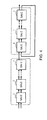
- the SALP 2 may be designed in such a manner that the output of SALC 1 is fed back to input of SALC 1 positioned at upstream by few stage, as shown in Fig. 4. Thereby, arithmetic operation between an operation result (obtained from downstream side SALC 1) and newly entered data (which is supplied to upstream side SALC 1) can be executed. Further, a complicated polynomial expression, such as executing arithmetical operation among values of the data being in mid course of process,can be achieved in one path.
- the SALP 2 can execute various macro commands in cooperation with a plurality of SALCs 1. An example of the operation in this case will be described in detail. A 4-bit multiplier will be described as a simple example hereinafter.
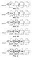
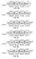
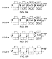
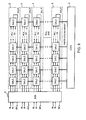
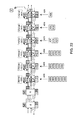
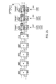
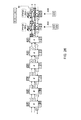
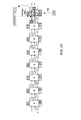
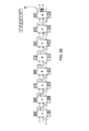
- Figs. 5A to 5P are diagrams showing states of the four SALCs 1 in the SALP 2 where those SALCs 1 are connected in a cascade fashion, as well as the contents of data in those states.
- the four-bit multiplication is conducted in such a manner that first data is inputted to the SALP 2 in a cycle 0 shown in Fig. 5A, and the four-bit multiplication is completed in a sixteenth cycle after the input of subsequent data, the decoding of an instruction, logic operation, latching, and output are conducted for each of clocks.
- a portion largest in area in each of the SALCs 1 denotes the decoder 10
- an upper portion of the decoder 10 is the carry latch circuit 16
- a lower and left side portion of the decoder 10 is the shift latch circuit 14
- a lower and right side portion thereof is the control latch circuit 15. Blanked portions and broken-line portions indicate that no data or like exists.
- Reference 0, A0 to A3, and B0 to B3 denote data to be subjected to operation, and SM0 to SM7 are operation result data.
- Characters in the decoder 10 represent instructions where "SET” is a data set that means the storage of data in the shift latch circuit 14 and the control latch circuit 15), “THR” is through that means that data is allowed to pass without being stored, and “ADS” is add & shift of data. Also, “carry” represents a carry bit which is latched in the carry latch circuit 16.
- the first cycle (cycle 0)
- the first data (0, A0) is inputted in a first SALC 1
- the operation result data (including "through") is outputted to a downstream SALC 1 after the instruction is decoded and the logic operation are conducted by the decoder 10.
- the operation is repeated in accordance with the instructions that are inputted simultaneously at a clock timing common to all of the SALCs 1, and the 4-bit multiplication result is finally obtained from the last SALC 1 as SM1 to SM7.
- the specific operation mode can be readily realized by only changing the instructions which are inputted to the respective SALCs 1.
- the instructions used in the float add are FSUB (subtract for float), SBS (subtract & set), CCHG (controlled change), CSFT (controlled shift), INV (inverse), REV (reverse), SFT (shift), OR, SUB (subtract & cnvset) and NSUB (subtract & RESET).
- the above-mentioned kinds of the instructions are exemplified, and other instructions can be also arbitrarily selected in accordance with the kinds of processing which are executable by the decoder 10.
- the SALP 2 can realize the processing performance proportional to a data range since the SALP 2 has the SALCs 1 as a basic structure and can conduct the logic operation in a flexible data range while appropriately changing a state in which the SALCs 1 are connected (for example, 8-bit operation has a performance which is twice of that of the 16-bit operation). Also, in the process, as to the data being processed, bit length of the data may be extended so as to keep the precision of arithmetic operation. Also, as to the data being processed, by deleting upper bit and/or lower bit, it is possible to effectively maintain, corresponding to the quality of data, significant digit number. In addition, an exponent and a mantissa are additionally processed to enable float operation.
- the throughput becomes 1/(data width) as compared with the parallel operation pipeline, but the area of the computing unit is reduced as much. If the reduced amount of the throughput is allocated to the parallel degree of the pipeline, the costs do not change in principle (if not taking the control into account). Moreover, because each stage of the pipeline is shorted, the processing speed can be made high as much.
- the SALP 2 can execute most of logic operations such as division, saturation operation, the sum-of products operation or polynomial expression.
- logic operations such as division, saturation operation, the sum-of products operation or polynomial expression.
- the costs increase in the operation of one element because the throughput is 1/(data width), but the costs become identical by allocating the operation elements in parallel in the operation of a large pieces of data.
- logic between the clocks can be cut for each of unit processing sizes (for example, 1 to 3 bits), and the frequency can be made significantly high since the so-called fan-out is very small.
- the judgment of the parallel line of the operation elements the judgment of the bits of a pipeline trailing line can be realized with a very small structure.
- a scalar process such that an address is calculated or a branch condition is calculated and a process where the processing regions are small, and a parameter changes for each of the regions can be realized by binding the regions.
- a plurality of SALPs 2 are employed, thereby being capable of structuring the arithmetic device that conducts the efficient logic operation.
- Fig. 6 is a structural diagram showing an arithmetic device including 256 SALPs 2 in which 32 SALCs (SALCs 1 shown in Fig. 1) are connected in cascade.
- Each of the SALPs 2 is connected in parallel with an external controller or a serial crossbar (SCB) 3 which is connected to a controller, a network or the like.
- An SCB 3 includes an address decoder and a plurality of crossbar switches and exchanges 256 lines in a small area, and can distribute data to a desired line by two phases consisting of address entering (control phase) and data entering (control phase) into a bus from the external controller or the like.
- Each of 256 SALPs 2 is inputted with an instruction array which is the group of n row of the instructions and m column of instructions (n x m instructions) from the instruction controller (iCON) 4, and the logic operation and the input/output lines of data are controlled independently.
- common instruction arrays are inputted at the same time.
- the common instruction arrays are inputted.
- the instruction arrays with individual contents may be individually inputted to the respective SALPs 2 to be inputted.
- the iCON 4 serially outputs each of the m columns to the first stage of the individual SALCs of respective SALPs, and for each of the outputted columns, allowing execution of an instruction of the column in the stage, deleting the executed instruction from the column, and outputting (or shift) the column to the next downstream stage.
- the iCON 4 repeats said processes of allowing execution, deleting the instruction, and outputting the column to the next stage until all the n instructions are deleted.
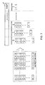
- the instruction array indicated by a broken-line block at a left side of Fig. 7 is hold in a memory of the iCON 4 (Fig. 6), sequentially read from the instructions at a right column of the broken-line block for each of the docks, and then inputted to the SALCs of the SALP 2.
- the executed instruction is deleted and inputted to a downstream SALC, and all of instructions at a subsequent column are inputted to the upstream SALC. This is repeated until all of the instructions are deleted.
- a fetch or data loop can be embedded in the instruction array.
- a complicated DFG described in the background of the invention can be described by one path, thereby simplifying the control mode of the arithmetic pipeline operation is achieved.
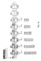
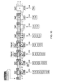
- the outputted operation result data becomes "01000101", and since its operation process is characteristic, a process of from an initial cycle to the output of the operation result data will be described with reference to the drawings.
- the prepared data is aligned in two lines as shown in Fig. 8B and sequentially inputted to the arithmetic device (SALP 2) from the data positioned most right side.
- SALP 2 arithmetic device
- MSBs are acquired four times at the time of acquiring data and then added to a leading portion of the data A.
- the added data does not affect the operation result.
- intermediate data is so-called intermediate data which is used in an operation process, which does not also affect the operation result.
- the instructions used in multiplication and addition in this example are of three kinds, i.e., "SET” (data set), "ADS” (addition and shift) and "THR".
- the instruction "SET" is to set reference data (data inputted to a downstream data input terminal) in the shift latch circuit 14, to set output data (data inputted to an upstream data input terminal) in the control latch circuit 15, and to set "0" in the carry latch circuit 16.
- the instruction "ADS" is to conduct only shift in a case where data latched in the control latch circuit 15 is "0", and to shift in other cases.
- the shift is to use the data latched in the shift latch circuit 14 as the reference data.
- the carry bit is changed (change carry).
- the instruction "THR" is to send inputted data (output data and reference data) to a downstream side without any changes.
- the arithmetic device is arranged in such a manner that a plurality of SALCs with a feedback function are connected at plural stages in a cascade manner in a SALPs 2, and a plurality of SALPs 2 are connected in parallel with each other in plural lines with respect to the SCB 3.
- the arithmetic operation made by the individual SALCs can be controlled by the instruction array from the iCON 4, individually, various logic operation (addition, subtraction, multiplication and division operations), the combination thereof, the saturation operation, the sum-of-products operation, the polynomial expression or the like can be realized by common hardware with ease and flexibility. For that reason, the arithmetic device according to this embodiment can cope with even a change in the application of the logic operation without any increase in the costs.
- the data arrangement, its execution procedure and so on can be arbitrarily installed into the instruction array, the data path can be advantageously simplified (linearly).
- the above-mentioned arithmetic device can particularly function as an effective tool with respect to logic operation where the amount of instructions are relatively large with respect to the input/output data.
- the arithmetic device can execute the complicated operation such as texture mapping without replacing any hardware. In this case, when the texture is not put in one fragment, surrounding fragments are entered plural times.
- the arithmetic device may include a lookup table that defines a plurality of functions, and a function of rewriting the contents of the lookup table by a throughput as much as the address cycle, thereby being capable of arithmetically calculating various functions in the multiplex manner.
Landscapes
- Engineering & Computer Science (AREA)
- Software Systems (AREA)
- Theoretical Computer Science (AREA)
- Physics & Mathematics (AREA)
- General Physics & Mathematics (AREA)
- General Engineering & Computer Science (AREA)
- Mathematical Physics (AREA)
- Computational Mathematics (AREA)
- Mathematical Analysis (AREA)
- Mathematical Optimization (AREA)
- Pure & Applied Mathematics (AREA)
- Advance Control (AREA)
- Executing Machine-Instructions (AREA)
- Multi Processors (AREA)
Abstract
Description
Claims (17)
- A serial operation pipeline, comprising:wherein at least one of the plurality of arithmetic-logic circuits include a first line for outputting data from an upstream stage to a downstream stage, a second line for feeding back the data from the downstream stage to the upstream stage, and a latch circuit that latches data on the respective lines.a plurality of arithmetic-logic circuits being connected in a cascade fashion, each of said arithmetic-logic circuits can be controlled independently and is operable together with other arithmetic-logic circuit,
- The serial operation pipeline as claimed in claim 1, wherein each of the plural arithmetic-logic circuits includes a decoder which executes a process including an operation corresponding to the contents of an externally supplied instruction, and outputs data representative of an execution result toward a desired line.
- The serial operation pipeline as claimed in claim 2, wherein said first line comprises a pair of lines for outputting a first output data and a second output data to the downstream stage, and
wherein the latch circuit includes a first data latch circuit that latches the first output data, a second data latch circuit that latches the second output data, a carry latch circuit that latches a carry resulting from an operation by the decoder for operation of a succeeding figure, and a shift latch circuit that delays one of the first output data and the second output data for a given period of time and can make reference to the other data. - The serial operation pipeline as claimed in claim 3, wherein the latch circuit further includes a reverse latch circuit that latches reverse data which is fed back to the upstream stage, and a control latch circuit that latches control data which controls an operation of the data latched in the first and second data latch circuits and the reverse latch circuit.
- The serial operation pipeline as claimed in claim 2, wherein the data to be processed by the decoder is data of a unit processing size.
- The serial operation pipeline as claimed in claim 5, wherein the data to be processed by the decoder has the shortest bit length which can be processed by one clock that determines the operation timing of the plurality of arithmetic-logic circuits.
- The serial operation pipeline as claimed in claim 1, wherein the first line comprises a forward line for outputting the data received from the upstream stage or an operation result based on the data received from the upstream stage to the downstream stage, and the second line comprises a backward line for outputting the data received from the downstream stage or an operation result based on the data received from the downstream stage to the upstream stage.
- An arithmetic device, comprising:wherein each of the plurality of serial operation pipelines comprises a plurality of arithmetic-logic circuits which are operable together with other arithmetic-logic circuit, and said arithmetic-logic circuits are connected in a cascade fashion, anda switch connection means that switchingly connects data input/output lines of plural systems;a plurality of serial operation pipelines which are connected in parallel with the switch connection means; andan instruction receive mechanism that receives an externally supplied instruction for the plurality of serial operation pipelines,
wherein each of the plurality of arithmetic-logic circuits comprises a forward line for outputting data received from the upstream stage or an operation result based on the data received from the upstream stage to the downstream stage, a backward line for feeding back the data received from the downstream stage or an operation result based on the data received from the downstream stage to the upstream stage, a decoder that executes a process corresponding to the inputted instruction and outputs an execution result to a desired line, and a latch circuit for synchronizing data output from each of the lines with respect to other arithmetic-logic circuit. - The arithmetic device as claimed in claim 8, further comprising a controller for outputting an instruction array, which is a group of the instructions comprising n rows of the instructions and m columns of instructions, said controller serially outputting each of the m columns to the first stage of the pipeline of the plurality of arithmetic-logic circuits, and for each of the outputted columns, allowing execution of an instruction of the column in the stage, deleting the executed instruction from the column, and outputting the column to the next downstream stage, said controller repeats said processes of allowing execution, deleting the instruction, and outputting the column to the next stage until all the n instructions are deleted.
- The arithmetic device as claimed in claim 9, wherein in the instruction array, an operation procedure for executing the operation through one path is determined.
- The arithmetic device as claimed in claim 8, wherein the forward line comprises a pair of lines for outputting the first output data and the second output data to the downstream stage, and the backward line comprises a line that outputs the reverse data, and
wherein the latch circuit in each of the plurality of arithmetic-logic circuits comprises:a first data latch circuit that latches the first output data;a second data latch circuit that latches a second output data;a reverse latch circuit that latches the reverse data;a carry latch circuit that latches a carry resulting from the operation for the operation of a succeeding figure;a shift latch circuit that delays one of the first output data and the second output data for a given period of time and enables reference to the other data; anda control latch circuit that latches control data for controlling the operation of the data latched in the first and second data latch circuits and the reverse latch circuit. - The arithmetic device as claimed in claim 8, wherein the data on the forward line and the data on the backward line in the decoder of each of the plurality of arithmetic-logic circuits are set as data of a unit processing size.
- The arithmetic device as claimed in claim 12, wherein the switch connection means, the plurality of serial operation pipelines and the instruction receive mechanism are installed in one semiconductor device.
- An arithmetic-logic circuit which is connectable in a cascade fashion as a structural element of a serial operation pipeline, the arithmetic-logic circuit comprising:one or a plurality of forward lines for outputting data received from an upstream stage of the serial operation pipeline or an operation result based on the data received from the upstream stage to a downstream stage;a backward line for feeding back the data received from the backward stage or an operation result based on the data received from the downstream stage to the upstream stage;a decoder that executes a process corresponding to an externally supplied instruction and outputs data representative of an execution result to a desired line; anda latch circuit for synchronizing with a timing of data output on each line with respect to another arithmetic-logic circuit.
- The arithmetic-logic circuit as claimed in claim 14, wherein the forward line comprises a pair of lines that output a first output data and a second output data, and the backward line comprises a line that outputs the reverse data, and
wherein the latch circuit comprises:a first data latch circuit that latches the first output data;a second data latch circuit that latches the second output data;a reverse latch circuit that latches the reverse data;a carry latch circuit that latches a carry resulting from an operation by the decoder for operation of a succeeding figure;a shift latch circuit that delays one of the first output data and the second output data for a given period of time and enables reference to the other output data; anda control latch circuit that latches a control data for controlling the operation of the data latched in the first and second data latch circuits and the reverse latch circuit. - An operation method using a serial operation pipeline comprises the steps of:providing a serial operation pipeline by connecting in a cascade fashion a plurality of arithmetic-logic circuits including one or plural first lines for outputting data to a downstream stage, and a second line for feeding back the data to an upstream stage, which conduct serial operation and can select a line to which data representative of an operation result is outputted, independently;executing, by an external controller connected to the serial operation pipeline;outputting an instruction array, which reflect a procedure of simultaneous execution through one path by the plurality of arithmetic-logic circuits, comprising n rows of the instructions and m columns of instructions, said controller serially outputting each of the m columns to the first stage of the pipeline of the plurality of arithmetic-logic circuits,allowing, for each of the outputted columns, execution of an instruction of the column in the stage,deleting the executed instruction from the column, andoutputting the column to the next downstream stage,further, said controller repeats said processes of allowing execution, deleting the instruction, and outputting the column to the next stage until all the n instructions are deleted.
- The operation method as claimed in claim 16, wherein the data on each line in the decoder of each of the plurality of arithmetic-logic circuits comprises data of a unit processing size.
Applications Claiming Priority (2)
| Application Number | Priority Date | Filing Date | Title |
|---|---|---|---|
| JP2002099202 | 2002-04-01 | ||
| JP2002099202A JP3719509B2 (en) | 2002-04-01 | 2002-04-01 | Serial arithmetic pipeline, arithmetic unit, arithmetic logic arithmetic circuit, and arithmetic method using serial arithmetic pipeline |
Publications (2)
| Publication Number | Publication Date |
|---|---|
| EP1351134A2 true EP1351134A2 (en) | 2003-10-08 |
| EP1351134A3 EP1351134A3 (en) | 2007-11-07 |
Family
ID=28035903
Family Applications (1)
| Application Number | Title | Priority Date | Filing Date |
|---|---|---|---|
| EP03006757A Withdrawn EP1351134A3 (en) | 2002-04-01 | 2003-03-25 | Superpipelined arithmetic-logic unit with feedback |
Country Status (3)
| Country | Link |
|---|---|
| US (1) | US7171535B2 (en) |
| EP (1) | EP1351134A3 (en) |
| JP (1) | JP3719509B2 (en) |
Cited By (1)
| Publication number | Priority date | Publication date | Assignee | Title |
|---|---|---|---|---|
| WO2015175173A1 (en) * | 2014-05-12 | 2015-11-19 | Qualcomm Incorporated | Utilizing pipeline registers as intermediate storage |
Families Citing this family (41)
| Publication number | Priority date | Publication date | Assignee | Title |
|---|---|---|---|---|
| EP1669868A4 (en) * | 2003-09-30 | 2009-03-25 | Sanyo Electric Co | Processor and integrated circuit comprising reconfigurable circuit, and processing method utilizing it |
| JP4478050B2 (en) * | 2005-03-18 | 2010-06-09 | 株式会社リコー | SIMD type microprocessor and data processing method |
| JP2006287675A (en) * | 2005-04-01 | 2006-10-19 | Renesas Technology Corp | Semiconductor integrated circuit |
| US7681017B2 (en) * | 2005-11-01 | 2010-03-16 | Lsi Corporation | Pseudo pipeline and pseudo pipelined SDRAM controller |
| CN101359284B (en) * | 2006-02-06 | 2011-05-11 | 威盛电子股份有限公司 | Multiply-accumulate unit and method for handling several different data formats |
| US20070226455A1 (en) * | 2006-03-13 | 2007-09-27 | Cooke Laurence H | Variable clocked heterogeneous serial array processor |
| US8656143B2 (en) | 2006-03-13 | 2014-02-18 | Laurence H. Cooke | Variable clocked heterogeneous serial array processor |
| JP2007249843A (en) * | 2006-03-17 | 2007-09-27 | Fujitsu Ltd | Reconfigurable computing device |
| EP2011018B1 (en) | 2006-04-12 | 2016-07-13 | Soft Machines, Inc. | Apparatus and method for processing an instruction matrix specifying parallel and dependent operations |
| US7870556B2 (en) * | 2006-05-16 | 2011-01-11 | Ab Initio Technology Llc | Managing computing resources in graph-based computations |
| US8346831B1 (en) * | 2006-07-25 | 2013-01-01 | Vivante Corporation | Systems and methods for computing mathematical functions |
| US20080052490A1 (en) * | 2006-08-28 | 2008-02-28 | Tableau, Llc | Computational resource array |
| US20080052429A1 (en) * | 2006-08-28 | 2008-02-28 | Tableau, Llc | Off-board computational resources |
| US20080126472A1 (en) * | 2006-08-28 | 2008-05-29 | Tableau, Llc | Computer communication |
| US20080052525A1 (en) * | 2006-08-28 | 2008-02-28 | Tableau, Llc | Password recovery |
| CN107368285B (en) | 2006-11-14 | 2020-10-09 | 英特尔公司 | Multi-threaded architecture |
| DE212007000102U1 (en) * | 2007-09-11 | 2010-03-18 | Core Logic, Inc. | Reconfigurable array processor for floating-point operations |
| EP2366144B1 (en) | 2008-10-15 | 2015-09-30 | Hyperion Core, Inc. | Sequential processor comprising an alu array |
| JP5590849B2 (en) * | 2009-10-08 | 2014-09-17 | キヤノン株式会社 | Data processing apparatus including parallel processing circuit having a plurality of processing modules, its control apparatus, its control method, and program |
| EP3156896B1 (en) | 2010-09-17 | 2020-04-08 | Soft Machines, Inc. | Single cycle multi-branch prediction including shadow cache for early far branch prediction |
| KR101620676B1 (en) | 2011-03-25 | 2016-05-23 | 소프트 머신즈, 인크. | Register file segments for supporting code block execution by using virtual cores instantiated by partitionable engines |
| CN108108188B (en) | 2011-03-25 | 2022-06-28 | 英特尔公司 | Memory fragment to support code block execution by using virtual cores instantiated by the partitionable engine |
| CN103547993B (en) | 2011-03-25 | 2018-06-26 | 英特尔公司 | By using the virtual core by divisible engine instance come execute instruction sequence code block |
| US9442772B2 (en) | 2011-05-20 | 2016-09-13 | Soft Machines Inc. | Global and local interconnect structure comprising routing matrix to support the execution of instruction sequences by a plurality of engines |
| CN107729267B (en) | 2011-05-20 | 2022-01-25 | 英特尔公司 | Distributed allocation of resources and interconnect structure for supporting execution of instruction sequences by multiple engines |
| KR101703401B1 (en) | 2011-11-22 | 2017-02-06 | 소프트 머신즈, 인크. | An accelerated code optimizer for a multiengine microprocessor |
| WO2013077876A1 (en) | 2011-11-22 | 2013-05-30 | Soft Machines, Inc. | A microprocessor accelerated code optimizer |
| WO2014150991A1 (en) | 2013-03-15 | 2014-09-25 | Soft Machines, Inc. | A method for implementing a reduced size register view data structure in a microprocessor |
| US9891924B2 (en) | 2013-03-15 | 2018-02-13 | Intel Corporation | Method for implementing a reduced size register view data structure in a microprocessor |
| US9569216B2 (en) | 2013-03-15 | 2017-02-14 | Soft Machines, Inc. | Method for populating a source view data structure by using register template snapshots |
| WO2014150971A1 (en) | 2013-03-15 | 2014-09-25 | Soft Machines, Inc. | A method for dependency broadcasting through a block organized source view data structure |
| US9811342B2 (en) | 2013-03-15 | 2017-11-07 | Intel Corporation | Method for performing dual dispatch of blocks and half blocks |
| EP2972845B1 (en) | 2013-03-15 | 2021-07-07 | Intel Corporation | A method for executing multithreaded instructions grouped onto blocks |
| US9904625B2 (en) | 2013-03-15 | 2018-02-27 | Intel Corporation | Methods, systems and apparatus for predicting the way of a set associative cache |
| US10275255B2 (en) | 2013-03-15 | 2019-04-30 | Intel Corporation | Method for dependency broadcasting through a source organized source view data structure |
| US10140138B2 (en) | 2013-03-15 | 2018-11-27 | Intel Corporation | Methods, systems and apparatus for supporting wide and efficient front-end operation with guest-architecture emulation |
| US9886279B2 (en) | 2013-03-15 | 2018-02-06 | Intel Corporation | Method for populating and instruction view data structure by using register template snapshots |
| WO2014150806A1 (en) | 2013-03-15 | 2014-09-25 | Soft Machines, Inc. | A method for populating register view data structure by using register template snapshots |
| WO2014151043A1 (en) | 2013-03-15 | 2014-09-25 | Soft Machines, Inc. | A method for emulating a guest centralized flag architecture by using a native distributed flag architecture |
| JP2017174291A (en) | 2016-03-25 | 2017-09-28 | ルネサスエレクトロニクス株式会社 | Image processing apparatus, image processing method, and automobile control apparatus |
| US11340875B2 (en) * | 2020-06-02 | 2022-05-24 | Sri International | Searchable storage of sequential application programs |
Family Cites Families (7)
| Publication number | Priority date | Publication date | Assignee | Title |
|---|---|---|---|---|
| US5179734A (en) * | 1984-03-02 | 1993-01-12 | Texas Instruments Incorporated | Threaded interpretive data processor |
| JPH0767063B2 (en) * | 1990-01-23 | 1995-07-19 | ヤマハ株式会社 | Digital signal processing circuit |
| US5038311A (en) * | 1990-08-10 | 1991-08-06 | General Electric Company | Pipelined fast fourier transform processor |
| JP3096387B2 (en) * | 1994-01-28 | 2000-10-10 | 三菱電機株式会社 | Numerical processing unit |
| JPH08137819A (en) * | 1994-11-04 | 1996-05-31 | Hitachi Ltd | Connection control device |
| US6044166A (en) * | 1995-01-17 | 2000-03-28 | Sarnoff Corporation | Parallel-pipelined image processing system |
| JPH10240558A (en) * | 1997-02-24 | 1998-09-11 | Hitachi Ltd | Control method of data processing device, data processing device, electron beam lithography device |
-
2002
- 2002-04-01 JP JP2002099202A patent/JP3719509B2/en not_active Expired - Fee Related
-
2003
- 2003-03-25 EP EP03006757A patent/EP1351134A3/en not_active Withdrawn
- 2003-04-01 US US10/404,182 patent/US7171535B2/en not_active Expired - Lifetime
Cited By (2)
| Publication number | Priority date | Publication date | Assignee | Title |
|---|---|---|---|---|
| WO2015175173A1 (en) * | 2014-05-12 | 2015-11-19 | Qualcomm Incorporated | Utilizing pipeline registers as intermediate storage |
| US9747104B2 (en) | 2014-05-12 | 2017-08-29 | Qualcomm Incorporated | Utilizing pipeline registers as intermediate storage |
Also Published As
| Publication number | Publication date |
|---|---|
| US20030200237A1 (en) | 2003-10-23 |
| EP1351134A3 (en) | 2007-11-07 |
| JP2003296096A (en) | 2003-10-17 |
| JP3719509B2 (en) | 2005-11-24 |
| US7171535B2 (en) | 2007-01-30 |
Similar Documents
| Publication | Publication Date | Title |
|---|---|---|
| US7171535B2 (en) | Serial operation pipeline, arithmetic device, arithmetic-logic circuit and operation method using the serial operation pipeline | |
| CN111353126B (en) | Block matrix multiplication system | |
| US6009451A (en) | Method for generating barrel shifter result flags directly from input data | |
| US8271571B2 (en) | Microprocessor | |
| US8024394B2 (en) | Dual mode floating point multiply accumulate unit | |
| US8468335B2 (en) | Reconfigurable system having plurality of basic function units with each unit having a plurality of multiplexers and other logics for performing at least one of a logic operation or arithmetic operation | |
| JP5956820B2 (en) | DSP block having embedded floating point structure | |
| KR100291383B1 (en) | Module calculation device and method supporting command for processing digital signal | |
| JP3578502B2 (en) | Method for performing parallel data processing on a single processor | |
| US5359548A (en) | Floating-point arithmetic system having multiple-input addition and subtraction means | |
| US20080059764A1 (en) | Integral parallel machine | |
| US5010511A (en) | Digit-serial linear combining apparatus useful in dividers | |
| CN1020170C (en) | high speed digital processor | |
| US5867413A (en) | Fast method of floating-point multiplication and accumulation | |
| US20020040427A1 (en) | Single instruction multiple data processing | |
| US5084834A (en) | Digit-serial linear combining apparatus | |
| US20060277247A1 (en) | Hybrid arithmetic logic unit | |
| KR102286101B1 (en) | Data processing apparatus and method for performing a narrowing-and-rounding arithmetic operation | |
| KR100900790B1 (en) | Method and Apparatus for arithmetic of configurable processor | |
| US7395294B1 (en) | Arithmetic logic unit | |
| JP4255475B2 (en) | Data-driven information processing device | |
| EP1936492A1 (en) | SIMD processor with reduction unit | |
| JP4413052B2 (en) | Data flow graph processing apparatus and processing apparatus | |
| EP2270647A1 (en) | Multi-bit carry chain | |
| JPH05324694A (en) | Reconstitutable parallel processor |
Legal Events
| Date | Code | Title | Description |
|---|---|---|---|
| PUAI | Public reference made under article 153(3) epc to a published international application that has entered the european phase |
Free format text: ORIGINAL CODE: 0009012 |
|
| AK | Designated contracting states |
Kind code of ref document: A2 Designated state(s): AT BE BG CH CY CZ DE DK EE ES FI FR GB GR HU IE IT LI LU MC NL PT RO SE SI SK TR |
|
| AX | Request for extension of the european patent |
Extension state: AL LT LV MK |
|
| PUAL | Search report despatched |
Free format text: ORIGINAL CODE: 0009013 |
|
| AK | Designated contracting states |
Kind code of ref document: A3 Designated state(s): AT BE BG CH CY CZ DE DK EE ES FI FR GB GR HU IE IT LI LU MC NL PT RO SE SI SK TR |
|
| AX | Request for extension of the european patent |
Extension state: AL LT LV MK |
|
| AKX | Designation fees paid | ||
| STAA | Information on the status of an ep patent application or granted ep patent |
Free format text: STATUS: THE APPLICATION IS DEEMED TO BE WITHDRAWN |
|
| 18D | Application deemed to be withdrawn |
Effective date: 20080508 |
|
| REG | Reference to a national code |
Ref country code: DE Ref legal event code: 8566 |