JP3578502B2 - Method for performing parallel data processing on a single processor - Google Patents
Method for performing parallel data processing on a single processor Download PDFInfo
- Publication number
- JP3578502B2 JP3578502B2 JP31267194A JP31267194A JP3578502B2 JP 3578502 B2 JP3578502 B2 JP 3578502B2 JP 31267194 A JP31267194 A JP 31267194A JP 31267194 A JP31267194 A JP 31267194A JP 3578502 B2 JP3578502 B2 JP 3578502B2
- Authority
- JP
- Japan
- Prior art keywords
- partial
- word
- bit
- multiplication
- partition
- Prior art date
- Legal status (The legal status is an assumption and is not a legal conclusion. Google has not performed a legal analysis and makes no representation as to the accuracy of the status listed.)
- Expired - Fee Related
Links
- 238000000034 method Methods 0.000 title claims description 26
- 238000012545 processing Methods 0.000 title description 24
- 230000004044 response Effects 0.000 claims description 9
- 238000005192 partition Methods 0.000 description 191
- 230000000295 complement effect Effects 0.000 description 14
- 230000000644 propagated effect Effects 0.000 description 12
- 238000010586 diagram Methods 0.000 description 10
- 238000000638 solvent extraction Methods 0.000 description 6
- 230000001902 propagating effect Effects 0.000 description 4
- 238000013461 design Methods 0.000 description 3
- XUIMIQQOPSSXEZ-UHFFFAOYSA-N Silicon Chemical compound [Si] XUIMIQQOPSSXEZ-UHFFFAOYSA-N 0.000 description 2
- 230000005540 biological transmission Effects 0.000 description 2
- 230000000694 effects Effects 0.000 description 2
- 238000012986 modification Methods 0.000 description 2
- 230000004048 modification Effects 0.000 description 2
- 229910052710 silicon Inorganic materials 0.000 description 2
- 239000010703 silicon Substances 0.000 description 2
- 102100039250 Essential MCU regulator, mitochondrial Human genes 0.000 description 1
- 101000813097 Homo sapiens Essential MCU regulator, mitochondrial Proteins 0.000 description 1
- 238000013459 approach Methods 0.000 description 1
- 230000008859 change Effects 0.000 description 1
- 230000008520 organization Effects 0.000 description 1
- 230000008569 process Effects 0.000 description 1
- 238000012546 transfer Methods 0.000 description 1
Images


Classifications
-
- G—PHYSICS
- G06—COMPUTING; CALCULATING OR COUNTING
- G06F—ELECTRIC DIGITAL DATA PROCESSING
- G06F7/00—Methods or arrangements for processing data by operating upon the order or content of the data handled
- G06F7/38—Methods or arrangements for performing computations using exclusively denominational number representation, e.g. using binary, ternary, decimal representation
- G06F7/48—Methods or arrangements for performing computations using exclusively denominational number representation, e.g. using binary, ternary, decimal representation using non-contact-making devices, e.g. tube, solid state device; using unspecified devices
- G06F7/52—Multiplying; Dividing
- G06F7/523—Multiplying only
- G06F7/53—Multiplying only in parallel-parallel fashion, i.e. both operands being entered in parallel
- G06F7/5324—Multiplying only in parallel-parallel fashion, i.e. both operands being entered in parallel partitioned, i.e. using repetitively a smaller parallel parallel multiplier or using an array of such smaller multipliers
-
- G—PHYSICS
- G06—COMPUTING; CALCULATING OR COUNTING
- G06F—ELECTRIC DIGITAL DATA PROCESSING
- G06F7/00—Methods or arrangements for processing data by operating upon the order or content of the data handled
- G06F7/38—Methods or arrangements for performing computations using exclusively denominational number representation, e.g. using binary, ternary, decimal representation
- G06F7/48—Methods or arrangements for performing computations using exclusively denominational number representation, e.g. using binary, ternary, decimal representation using non-contact-making devices, e.g. tube, solid state device; using unspecified devices
- G06F7/483—Computations with numbers represented by a non-linear combination of denominational numbers, e.g. rational numbers, logarithmic number system or floating-point numbers
-
- G—PHYSICS
- G06—COMPUTING; CALCULATING OR COUNTING
- G06F—ELECTRIC DIGITAL DATA PROCESSING
- G06F7/00—Methods or arrangements for processing data by operating upon the order or content of the data handled
- G06F7/38—Methods or arrangements for performing computations using exclusively denominational number representation, e.g. using binary, ternary, decimal representation
- G06F7/48—Methods or arrangements for performing computations using exclusively denominational number representation, e.g. using binary, ternary, decimal representation using non-contact-making devices, e.g. tube, solid state device; using unspecified devices
- G06F7/50—Adding; Subtracting
- G06F7/505—Adding; Subtracting in bit-parallel fashion, i.e. having a different digit-handling circuit for each denomination
- G06F7/506—Adding; Subtracting in bit-parallel fashion, i.e. having a different digit-handling circuit for each denomination with simultaneous carry generation for, or propagation over, two or more stages
- G06F7/508—Adding; Subtracting in bit-parallel fashion, i.e. having a different digit-handling circuit for each denomination with simultaneous carry generation for, or propagation over, two or more stages using carry look-ahead circuits
-
- G—PHYSICS
- G06—COMPUTING; CALCULATING OR COUNTING
- G06F—ELECTRIC DIGITAL DATA PROCESSING
- G06F9/00—Arrangements for program control, e.g. control units
- G06F9/06—Arrangements for program control, e.g. control units using stored programs, i.e. using an internal store of processing equipment to receive or retain programs
- G06F9/30—Arrangements for executing machine instructions, e.g. instruction decode
- G06F9/30003—Arrangements for executing specific machine instructions
- G06F9/30007—Arrangements for executing specific machine instructions to perform operations on data operands
- G06F9/3001—Arithmetic instructions
- G06F9/30014—Arithmetic instructions with variable precision
-
- G—PHYSICS
- G06—COMPUTING; CALCULATING OR COUNTING
- G06F—ELECTRIC DIGITAL DATA PROCESSING
- G06F9/00—Arrangements for program control, e.g. control units
- G06F9/06—Arrangements for program control, e.g. control units using stored programs, i.e. using an internal store of processing equipment to receive or retain programs
- G06F9/30—Arrangements for executing machine instructions, e.g. instruction decode
- G06F9/30003—Arrangements for executing specific machine instructions
- G06F9/30007—Arrangements for executing specific machine instructions to perform operations on data operands
- G06F9/30036—Instructions to perform operations on packed data, e.g. vector, tile or matrix operations
-
- G—PHYSICS
- G06—COMPUTING; CALCULATING OR COUNTING
- G06F—ELECTRIC DIGITAL DATA PROCESSING
- G06F2207/00—Indexing scheme relating to methods or arrangements for processing data by operating upon the order or content of the data handled
- G06F2207/38—Indexing scheme relating to groups G06F7/38 - G06F7/575
- G06F2207/3804—Details
- G06F2207/3808—Details concerning the type of numbers or the way they are handled
- G06F2207/3828—Multigauge devices, i.e. capable of handling packed numbers without unpacking them
Description
【0001】
【産業上の利用分野】
本発明は、単一プロセッサにおける並列データ処理に関するものである。
【0002】
【従来の技術】
一般に、単一プロセッサ・システムは、2つのオペランドに順次演算を施す。例えば、32ビットコンピュータの場合、各整数オペランドは、32ビットである。64ビット・コンピュータの場合、各整数オペランドは、64ビットである。従って、64ビット・コンピュータにおける整数「加算」命令では、2つの64ビット整数オペランドを加算して、64ビットの整数結果が得られる。ほとんどのパイプラインで形成された64ビット・プロセッサでは、64ビット加算命令に、1サイクルの実行時間を要する。
【0003】
多くの例において、オペランドの直接関連する範囲は16ビット又はそれ以下である。しかし、現在の32ビットまたは64ビット・コンピュータにおいて、1対の16ビット・オペランドの演算を施すには今まで通り完全な命令が必要になる。従って、16ビット・オペランドに演算を施すのに必要な実行サイクル数は、32ビット・コンピュータにおける2つの32ビット・オペランド、または64ビット・コンピュータにおける2つの64ビット・オペランドに演算を施すのに必要な実行サイクル数と同じになる。
【0004】
先行技術の場合、並列データ処理には、それぞれ、フル・ワード長のデータを取り扱うことが可能な機能毎のユニットからなる、機能毎のユニットの複製品を作ることが必要とされた。例えば、1966年12月の、Proceedings of IEEE、第54巻、1901〜1909ページにおける、Michael FlynnによるVery High−Speed Computing Systemsを参照されたい。
【0005】
【発明が解決しようとする課題】
しかし、こうした並列処理の実施は、必要なハードウェア及び設計の複雑さの両方に関連して、コストが高くつく。
【0006】
【課題を解決するための手段】
本発明の望ましい実施例によれば、単一プロセッサ内における並列データ処理を可能にするシステムが提供される。データの並列処理を可能にするため、シフタのような処理システム内における論理演算装置または他の演算実行エンティティが区分化される。各パーティション内で、演算が実施される。フル・ワード長のオペランドに対する演算を実施すべき場合には、並列処理は行われない。従って、パーティション間における境界を越えてデータを自由に伝搬させることが可能である。1フル・ワード長未満の複数のオペランドを利用して、並列に演算を実施する場合には、パーティション間における少なくとも1つの境界を越えてデータが伝搬しないようにする。
【0007】
例えば、演算が加算演算(例えば、2の補数加算)の場合、複数のパーティションが、それぞれ、加算演算を実施する。フル・ワード長のオペランドに加算を施すべき場合には、パーティション間における桁上げの伝播が可能になる。1フル・ワード長より短い複数のオペランド集合に並列加算演算を施す場合には、パーティション間における少なくとも1つの境界を越える桁上げの伝播が阻止される。
【0008】
同様に、演算がシフトの場合、複数のパーティションが、それぞれ、シフト演算を実施する。フル・ワード長のオペランドにシフトを施すべき場合には、パーティション間におけるシフトが可能になる。1フル・ワード長より短い複数のオペランドを利用して、並列に演算を施す場合には、パーティション間における少なくとも1つの境界を越えるシフトが阻止される。
【0009】
また、本発明の望ましい実施例によれば、乗算器は、全ワード被乗数の乗算とサブ・ワード被乗数の並列乗算の両方を実施する。例えば、論理ANDゲート(またはその同等物)のアレイといった回路要素が、部分積を発生する。部分積和回路要素が、部分積を合計することによって、結果が得られる。部分積ゲート手段が、サブ・ワード被乗数の並列乗算の選択に応答して、選択された部分積の値を強制的にゼロにし、この結果、サブ・ワード被乗数の並列乗算が実施される。乗算器が全ワード乗算を実施している間、部分積の値が強制的にゼロにされることはない。部分積ゲート手段は、例えば、論理ANDゲートの少なくとも一部に対する第3の入力を利用して実施することが可能である。
【0010】
本発明によれば、オペランドがフル・ワード長より短い場合における並列処理演算を容易化することによって、単一プロセッサ・システムの性能を大幅に高めることが可能になる。並列処理のこの低コストの利用によって、プロセッサ・チップにおけるシリコン・スペースまたは設計の複雑さにあまりコストを費やすことなく、このタイプのデータ並列処理を利用可能な計算に関する性能が大幅に向上する。
【0011】
【実施例】
図1には、本発明の望ましい実施例による、プロセッサ内における演算実行データ経路の略ブロック図が示されている。近く行われることになる演算のオペランド及び実施済みの演算の結果は、汎用レジスタ25に記憶される。演算が実施される際には、汎用レジスタ25内の第1のレジスタに記憶された第1のオペランドが、第1のソース・バス21に送り出される。演算に別のオペランドが必要な場合には、汎用レジスタ25内の第2のレジスタに記憶されている第2のオペランドが、第2のソース・バス22に送り出される。
【0012】
演算の実施後、結果は、結果バス23に送り出され、汎用レジスタ25内のレジスタにロードされる。演算は、論理演算装置(ALU)26またはシフタ29によって実施される。プリ・シフタ27及び補数回路要素28のそれぞれを利用して、ALU26が受信する前に、オペランドに修正を加えることが可能である。本発明と同様に構成された、単一プロセッサ・システムのアーキテクチャに関する一般的背景については、1989年1月の、IEEE Computer、第22巻、第1号、78〜91ページにおける、Ruby B.LeeよるPrecision Architectureを参照されたい。
【0013】
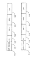
本発明の望ましい実施例によれば、ALUを区分化して、並列データ処理を行うことが可能である。例えば、図2には、2つのパーティションに分割されたALU26が示されている。第1のパーティション41は、第1のオペランドの下位ビット42、及び、第2のオペランドの下位ビット43に演算を施して、下位ビットの結果44を求める。第2のパーティション51は、第1のオペランドの上位ビット52、及び、第2のオペランドの上位ビット53に演算を施して、上位ビットの結果54を求める。
【0014】
セレクタ50を利用することによって、制御入力49に応答して、データ経路45の情報を第1のパーティション41から第2のパーティション51に伝搬できるようにするか、あるいは、第1のパーティション41から第2のパーティション51への伝搬前に、データ経路45の情報を遮断することが可能になる。すなわち、フル・ワード・オペランドに対して実施される算術演算の場合、情報は、セレクタ50を介して第1のパーティション41から第2のパーティション51に伝搬させることが可能である。ハーフ・ワード・オペランドに対して並列算術演算が実施される場合には、セレクタ50によって、第1のパーティション41から第2のパーティション51への情報の伝搬が阻止される。一般に、論理演算の場合、第1のパーティション41から第2のパーティション51への情報の伝搬は生じない。
【0015】
例えば、32ビット幅のデータ経路を備えたコンピュータの場合、各フル・ワード・オペランドは、32ビットである。従って、32ビットのフル・ワード・オペランドを利用して演算を行う場合、セレクタ50は、セレクタ50を介した、第1のパーティション41から第2のパーティション51への情報伝搬を可能にする。16ビットのハーフ・ワード・オペランドを利用して2つの並列演算を行う場合、セレクタ50は、セレクタ50を介した、第1のパーティション41から第2のパーティション51への情報伝搬を阻止する。代わりに、ライン59の値がパーティション51に送られる。「加算」の実施時には、論理0が、入力ライン59におきかわる。「減算」の実施時には、論理1が、入力ライン59におきかわる。
【0016】
本発明の望ましい実施例の場合、図1に示すALUによって実施される一般的な算術演算は、2の補数加算である。当該技術の熟練者には明らかなように、ALUにおいて2の補数加算演算を実施する前に、2の補数回路要素28を利用して、あるオペランドに対する2の補数演算を実施することによって、2の補数減算が実施される。また、ALUにおいて2の補数加算演算を実施する前に、プリ・シフタ27を利用して、オペランドのプリ・シフトを行うことによって、シフト及び加算演算が実施される。
【0017】
図3には、本発明の望ましい実施例による、ALU26内における桁上げ伝播加算を行う2の補数加算器の実施例が示されている。代替案では、ALU26に、桁上げ先見加算を行う2の補数加算器が含まれる。ハーフ加算器60は、第1のオペランドの単一ビットX0及び第2のオペランドの単一ビットY0を受信する。ハーフ加算器60は、和ビットZ0及び桁上げビットC0を送り出す。フル加算器61は、第1のオペランドの単一ビットX1、第2のオペランドの単一ビットY1、及び、桁上げビットC0を受け取る。フル加算器61は、和ビットZ1及び桁上げビットC1を送り出す。フル加算器65は、第1のオペランドの単一ビットXiー1、第2のオペランドの単一ビットYiー1、及び、先行加算器(すなわち、不図示のCiー2)からの桁上げビットを受け取る。フル加算器65は、和ビットZiー1及び桁上げビットCiー1を送り出す。フル加算器66は、第1のオペランドの単一ビットXi及び第2のオペランドの単一ビットYiを受け取る。許可ビット49の値によって、フル加算器66は、セレクタ50(または、当該技術の通常の技術者であれば理解し得る同等の論理回路要素)を介して桁上げビットCiを受信する。フル加算器69は、第1のオペランドの単一ビットXjー1、第2のオペランドの単一ビットYjー1、及び、先行加算器(不図示)からの桁上げビットを受信する。フル加算器69は、和ビットZj−1及び桁上げビットCj−1を送り出す。
【0018】
図3に示す加算器の実施例の場合、「j」は、データ経路のサイズ、及び、フル・ワード演算のビット長である。また、「i」は、「j」を2で割った値に等しい。例えば、「j」が32に等しければ、「i」は16に等しい。
【0019】
セレクタ50は、図3にも示されている。「j」ビットのフル・ワード・オペランドを利用して演算を行う場合、許可ビット49は、論理1に等しく、桁上げがセレクタ50を介してフル加算器66に伝播するのを可能にする。「i」ビットのハーフ・ワード・オペランドを利用して2つの並列演算を実施する場合、許可ビット49は論理ゼロに等しく、桁上げがセレクタ50を介してフル加算器66に伝播するのを阻止する。代わりに、ライン59の値が、フル加算器66に送られる。「加算」の実施時には、論理0が入力ライン59におきかわる。「減算」の実施時には、論理1が入力ライン59におきかわる。
【0020】
図2及び図3には、2つのパーティションを備えたALU26の実施例が示されているが、本発明の他の望ましい実施例に基づいて設計されたALUの場合、ALUをさまざまに区分化することが可能である。例えば、図4には、本発明の望ましい代替実施例に基づくALU26の代替略ブロック図が示されている。図4では、ALU6は、4つのパーティションに分割されている。第1のパーティション71は、第1のオペランドの下位ビット72及び第2のオペランドの下位ビット73に演算を施し、下位ビットの結果74を求める。第2のパーティション81は、第1のオペランドのビット82及び第2のオペランドのビット83に演算を施し、結果ビット84を求める。第3のパーティション91は、第1のオペランドのビット92及び第2のオペランドのビット93に演算を施し、結果ビット94を求める。第4のパーティション101は、第1のオペランドの上位ビット102及び第2のオペランドの上位ビット103に演算を施し、上位ビットの結果104を求める。
【0021】
セレクタ80を利用して、制御入力79に応答し、第1のパーティション71から第2のパーティション81へのデータ経路75における情報の伝搬を可能にするか、あるいは、第1のパーティション71から第2のパーティション81へ伝搬する前に、データ経路75の情報を遮断する。すなわち、フル・ワード・オペランドまたはハーフ・ワード・オペランドに対して実施される算術演算の場合、セレクタ80を介した、第1のパーティション71から第2のパーティション81への情報伝搬が可能になる。クォータ・ワード・オペランドに対する並列算術演算を実施する場合、セレクタ80は、第1のパーティション71から第2のパーティション81への情報の伝搬を阻止する。代わりに、ライン88の値がパーティション81に送られる。「加算」の実施時には、ライン88で論理0が伝送される。「減算」の実施時には、ライン88で論理1が伝送される。一般に、論理演算の場合、パーティション間における情報の伝搬は生じない。
【0022】
セレクタ90を利用して、制御入力89に応答し、第2のパーティション81から第3のパーティション91へのデータ経路85における情報の伝搬を可能にするか、あるいは、第2のパーティション81から第3のパーティション91へ伝搬する前に、データ経路75の情報を遮断する。すなわち、フル・ワード・オペランドに対して実施される算術演算の場合、セレクタ90を介した、第2のパーティション81から第3のパーティション91への情報伝搬が可能になる。クォータ・ワード・オペランドまたはハーフ・ワード・オペランドに対する並列算術演算を実施する場合、セレクタ90は、第2のパーティション81から第3のパーティション91への情報の伝搬を阻止する。代わりに、ライン98の値がパーティション91に送られる。「加算」の実施時には、ライン98で論理0が伝送される。「減算」の実施時には、ライン98で論理1が伝送される。
【0023】
セレクタ100を利用して、制御入力99に応答し、第3のパーティション91から第4のパーティション101へのデータ経路95における情報の伝搬を可能にするか、あるいは、第3のパーティション91から第4のパーティション101へ伝搬する前に、データ経路75の情報を遮断する。すなわち、フル・ワード・オペランド及びハーフ・ワード・オペランドに対して実施される算術演算の場合、セレクタ100を介した、第3のパーティション91から第4のパーティション101への情報伝搬が可能になる。クォータ・ワード・オペランドに対する並列算術演算を実施する場合、セレクタ100は、第3のパーティション91から第4のパーティション101への情報の伝搬を阻止する。代わりに、ライン108の値がパーティション101に送られる。「加算」の実施時には、ライン108で論理0が伝送される。「減算」の実施時には、ライン108で論理1が伝送される。
【0024】
例えば、64ビット幅のデータ経路を備えるコンピュータの場合、各フル・ワード・オペランドは64ビットである。従って、64ビットのフル・ワード・オペランドを利用して演算を実施する場合、セレクタ80は、セレクタ80を介した、第1のパーティション71から第2のパーティション81への情報の伝搬を可能にし、セレクタ90は、セレクタ90を介した、第2のパーティション81から第3のパーティション91への情報の伝搬を可能にし、セレクタ100は、セレクタ100を介した、第3のパーティション91から第4のパーティション101への情報の伝搬を可能にする。32ビットのハーフ・ワード・オペランドを利用して2つの並列演算を実施する場合、セレクタ80は、セレクタ80を介した、第1のパーティション71から第2のパーティション81への情報の伝搬を可能にし、セレクタ90は、セレクタ90を介した、第2のパーティション81から第3のパーティション91への情報の伝搬を阻止し、セレクタ100は、セレクタ100を介した、第3のパーティション91から第4のパーティション101への情報の伝搬を可能にする。16ビットのクォータ・ワード・オペランドを利用して4つの並列演算を実施する場合、セレクタ80は、セレクタ80を介した、第1のパーティション71から第2のパーティション81への情報の伝搬を阻止し、セレクタ90は、セレクタ90を介した、第2のパーティション81から第3のパーティション91への情報の伝搬を阻止し、セレクタ100は、セレクタ100を介した、第3のパーティション91から第4のパーティション101への情報の伝搬を阻止する。
【0025】
図5には、本発明のもう1つの望ましい代替実施例に基づく、ALU26のもう1つの代替略ブロック図が示されている。図5の場合、ALU26は、それぞれ、1ビット幅のパーティションに分割される。第1のパーティション111は、第1のオペランドの下位ビット112及び第2のオペランドの下位ビット113に演算を施し、下位結果ビット114を求める。第2のパーティション121は、第1のオペランドのビット122及び第2のオペランドのビット123に演算を施し、結果ビット124を求める。パーティション131は、第1のオペランドのビット132及び第2のオペランドのビット133に演算を施し、結果ビット134を求める。パーティション141は、第1のオペランドのビット142及び第2のオペランドのビット143に演算を施し、結果ビット144を求める。パーティション151は、第1のオペランドの上位ビット152及び第2のオペランドの上位ビット153に演算を施し、上位結果ビット154を求める。
【0026】
セレクタ120を利用して、制御入力119に応答し、第1のパーティション111から第2のパーティション121へのデータ経路115における情報の伝搬を可能にするか、あるいは、第1のパーティション111から第2のパーティション121へ伝搬する前に、データ経路115の情報を遮断する。データが遮断されると、ライン128の値がパーティション121に送られる。「加算」の実施時には、ライン128で論理0が伝送される。「減算」の実施時には、ライン128で論理1が伝送される。
【0027】
セレクタ130を利用して、制御入力129に応答し、あるデータ経路におけるすぐ前のパーティション(不図示)からパーティション131への、前記すぐ前のパーティションからの情報の伝搬を可能にするか、あるいは、パーティション131に伝搬する前に、該データ経路における前記すぐ前のパーティションからの情報を遮断する。データが遮断されると、ライン138の値がパーティション131に送られる。「加算」の実施時には、ライン138で論理0が伝送される。「減算」の実施時には、ライン138で論理1が伝送される。
【0028】
セレクタ140を利用して、制御入力139に応答し、パーティション131からパーティション141へのデータ・ライン135における情報の伝搬を可能にするか、あるいは、パーティション131からパーティション141へ伝搬する前に、データ経路135の情報を遮断する。データが遮断されると、ライン148の値がパーティション141に送られる。「加算」の実施時には、ライン148で論理0が伝送される。「減算」の実施時には、ライン148で論理1が伝送される。
【0029】
セレクタ150を利用して、制御入力149に応答し、あるデータ経路におけるすぐ前のパーティション(不図示)からパーティション151への、前記すぐ前のパーティションからの情報の伝搬を可能にするか、あるいは、パーティション151に伝搬する前に、該データ経路における前記すぐ前のパーティションからの情報を遮断する。データが遮断されると、ライン158の値がパーティション151に送られる。「加算」の実施時には、ライン158で論理0が伝送される。「減算」の実施時には、ライン158で論理1が伝送される。
【0030】
セレクタに対する制御入力を利用することによって、可変長オペランドの並列処理を可能にすることができる。例えば、64ビット幅のデータ経路を備えた処理システムの場合、制御入力は、2つの16ビット算術演算及び4つの8ビット算術演算の並列処理が、全て、同時に実施されるように選択することが可能である。さらに、合計しても、そのワード・サイズまでにしかならない任意のビット組み合わせを利用することも可能である。例えば、17ビット、3ビット、16ビット、12ビット、5ビット、及び、11ビットの算術演算を同時に実施することも可能である。
【0031】
上述の原理は、桁上げ先見加算器にも当てはまる。例えば、図10には、本発明の別の望ましい実施例に基づく、ALU26内の桁上げ先見を伴う、2の補数加算器の実施例が示されている。桁上げ先見回路470によって、加算器の桁上げが生じる。ハーフ加算器460は、第1のオペランドの単一ビットX0及び第2のオペランドの単一ビットY0を受信する。ハーフ加算器460は、和ビットZ0を送り出す。フル加算器461は、第1のオペランドの単一ビットX1、第2のオペランドの単一ビットY1、及び、桁上げビットC0を受信する。フル加算器461は、和ビットZ1を送り出す。フル加算器465は、第1のオペランドの単一ビットXi−1、第2のオペランドの単一ビットYi−1、及び、桁上げビットCi−2を受信する。フル加算器465は、和ビットZi−1を送り出す。フル加算器466は、第1のオペランドの単一ビットXi、第2のオペランドの単一ビットYi、及び、桁上げビットCi−1を受信する。フル加算器466は、和ビットZiを送り出す。フル加算器469は、第1のオペランドの単一ビットXj− 1、第2のオペランドの単一ビットYj−1、及び、桁上げビットCj−2を受信する。フル加算器469は、和ビットZj−1を送り出す。
【0032】
図10に示す加算器の実施例の場合、「j」は、データ経路のサイズ及びフル・ワード演算のビット長である。また、「i」は、「j」を2で割った値に等しい。例えば、「j」が32に等しいと、「i」は16に等しい。代わりに、jが32に等しい場合、iを32未満の任意の整数に等しくなるようにすることも可能である。
【0033】
「j」ビットのフル・ワード・オペランドを利用して演算を実施する場合、許可ビット452は、論理1に等しく、全ての桁上げの伝播を可能にする。ビットiとi+1の間で区分された「i」ビットのサブ・ワード・オペランドを利用して2つの並列演算を実施する場合、許可ビット452は、論理0に等しく、パーティション境界を越える桁上げの伝播を阻止する。代わりに、ライン451の値が、フル加算器466に送られる値として利用される。「加算」の実施時には、入力ライン451で論理0が伝送される。「減算」の実施時には、入力ライン451で論理1が伝送される。
【0034】
桁上げ先見加算器の働きは、当該技術において周知のところである。例えば、A[i]が入力の1ビットであり、B[i]が他の入力の1ビットであり、S[i]が加算器からの和の1ビットであると仮定する。加算器からの和の1ビットは、下記の式1によって示される。
【0035】
【数1】

式1において、C[i−1]は、桁上げ先見加算器の先行ビットからの桁上げである。桁上げ先見加算器は、これらの桁上げビットを素早く発生するのに有効である。
【0037】
G[i]が、このビットによって桁上げを発生させるべきであることを示す信号であり、P[i]が、先行ビットからこのビットの出力に桁上げが伝播する可能性のあることを示す信号であると仮定する。これらは、下記の式2によって決まる。
【0038】
【数2】
従って、桁上げ先見加算器内における4ビットの場合、桁上げビットは、下記の式3のように発生させることが可能である。
【0040】
【数3】
上記式3において、「*」は、論理AND演算に相当し、「+」は、論理OR演算に相当する。
【0042】
本発明の望ましい実施例を実行する場合、発生G[i]及び伝播P[i]が強制的に偽にされると、桁上げは、特定のビットで停止する。例えば、上記式3の場合、G[i−3]及びP[i−3]が偽の場合、C[i−3]は偽になり、C[i−4]は、C[i−2]、C[i−1]、及び、C[i]の値に影響を及ぼすことはできない。同様に、G[i−2]及びP[i−2]が偽の場合、C[i−2]は偽になり、G[i−3]及びP[i−3]及びC[i−4]は、C[i−1]及びC[i]の値に影響を及ぼすことはできない。
【0043】
M[i]が、1の場合、ビット[i]とビット[i+1]との桁上げ連鎖をブレークするマスク・ビットであると仮定すると、新しい式4は、下記のように生成することが可能である。
【0044】
【数4】
M[i]が1の場合、桁上げは、ビット[i]から発生することができないか、あるいは、ビット[i]を介して伝播することができない。
【0046】
キャリ・インに関して、オペランドの一方の1の補数を生成し、もう一方のオペランドに加算することによる減算(2の補数演算)の場合、M[i]が1であれば、あるビットにおいて強制的に桁上げを発生しなければならない。
【0047】
Fが、真の場合、M[i]が1であれば、あるビットにおいて強制的に桁上げを発生させる信号であると仮定する。Gs[i]及びPs[i]に関する式は、下記の式5に示すようになる。
【0048】
【数5】
M[i]が1の場合、Gs[i]の値はFによって決まる。M[i]が1の場合、Gs[i]の値は、前述のように、A[i]及びB[i]によって決まる。この伝播は、F信号によって強制する必要はない。
【0050】
キャリ・アウトの式は、下記の式6によって示される。
【0051】
【数6】
当該技術の熟練者には明らかなように、本発明の原理は、コンピュータ・システムALU内の算術演算に限定されるものではない。例えば、ALUに示される区分化は、データに基づいて機能するコンピュータ・システム内の他のエンティティにも拡張することが可能である。例えば、図6には、プリ・シフタ27において具現化された本発明が示されている。本発明の同じ実施例は、シフタ29の実施にも利用することが可能である。プリ・シフタ27及びシフタ29を区分化することによって、例えば、並列シフト・加算演算、及び、並列シフト演算の実施が可能になる。
【0053】
プリ・シフタ27には、図示のように、シフト・レジスタ・1ビット・スライス160、シフト・レジスタ・1ビット・スライス161、シフト・レジスタ・1ビット・スライス165、シフト・レジスタ・1ビット・スライス166、及び、シフト・レジスタ・1ビット・スライス169が含まれている。
【0054】
データを左にシフトする場合には、一般に、論理値が0の、入力171におけるデータが、シフト・レジスタ・1ビット・スライス160に対する入力として利用される。データを右にシフトする場合には、セレクタ175が、制御入力182に応答し、入力181におけるデータ(論理値0または論理値1)を選択するか、あるいは、シフト・レジスタ・1ビット・スライス169によって現在記憶されている値を選択して、シフト・レジスタ・1ビット・スライス169に対する入力とする。
【0055】
シフタを区分化すべき場所がどこであれ、シフタには、追加セレクタが追加される。例えば、図6には、シフト・レジスタ・1ビット・スライス165とシフト・レジスタ・1ビット・スライス166の間で区分化されたシフタが示されている。そこには、セレクタ174及びセレクタ173が追加されている。区分化オペランドに対するシフト演算に関して、データが左にシフトされる場合には、セレクタ173は、制御入力185に応答して、一般には論理値0の、入力172のデータを選択し、シフト・レジスタ・1ビット・スライス166として利用する。フル・ワード・オペランドに対するシフト演算に関して、データが左にシフトされる場合には、セレクタ173は、シフト・レジスタ・1ビット・スライス165からの出力を選択し、シフト・レジスタ・1ビット・スライス166に対する入力として利用する。
【0056】
区分化オペランドに対するシフト演算に関して、データが右にシフトされる場合には、セレクタ174は、制御入力184に応答し、入力183におけるデータ(論理値0または論理値1)を選択するか、あるいは、シフト・レジスタ・1ビット・スライス166によって現在記憶されている値を選択して、シフト・レジスタ・1ビット・スライス165に対する入力とする。フル・ワード・オペランドに対するシフト演算に関して、データが右にシフトされる場合には、セレクタ174は、シフト・レジスタ・1ビット・スライス166からの出力を選択し、シフト・レジスタ・1ビット・スライス165に対する入力として利用する。
【0057】
図6には、パーティションが2つだけのシフタが示されている。ALUにおけるパーティションに関する以上の説明から明らかなように、シフタは、さまざまなやり方で区分化することが可能である。例えば、64ビットのシフタは、2、4、8、16、32、または、64ビットの等サイズのパーティションに区分化することが可能である。さらに、パーティションが、それぞれ、等しいビット数で動作するのは、本発明の要件ではない。
【0058】
上記実施例では、一連の1ビット・スライスから構成されるシフト・レジスタとして実施された、プリ・シフタ27及びシフタ29が示されているが、望ましい代替実施例には、マルチプレクサで実施されるプリ・シフタ及びシフタがある。一般に、プリ・シフタ27は、通常、例えば、せいぜい、0、1、2、3、または、4ビットといった小ビット数ずつしかシフトすることができないので、1レベルのマルチプレクサによって実施される。シフタ29は、一般に、各レベルが4対1マルチプレクサである、3レベルのマルチプレクサによって実施される。例えば、64ビット・シフタ29の場合、第1レベルのマルチプレクサは、0、16、32、または、48ビットのシフトを行う。第2レベルのマルチプレクサは、0、4、8、または、12ビットのシフトを行うことができる。第3レベルのマルチプレクサは、0、1、2、または、3ビットのシフトを行うことができる。これによって、0〜63の任意のビット数のシフトが行えることになる。3段のマルチプレクサから構成されるこうしたシフタの場合、1ビット・スライスを識別することも可能である。しかし、当該技術の熟練者には明らかなように、3つのマルチプレクサ段の1つ以上において、任意の2ビット間におけるシフトをブロックすることが必要になる可能性がある。
【0059】
本発明の原理は、コンピュータ・システムにおける他の構成要素にも拡張することが可能である。例えば、乗算器は、本発明の望ましい実施例に従い、全ワード乗算以外に、部分ワード並列乗算も行えるように実施することが可能である。
【0060】
例えば、図7には、先行技術による4ビット乗算器が示されている。乗算器が、4ビットの最初の被乗数X3X2X1X0(基数2)と4ビットの第2の被乗数Y3Y2Y1Y0(基数2)を掛け合わせることによって、8ビットの結果Z7Z6Z5Z4Z3Z2Z1Z0(基数2)が得られる。当該技術の熟練者には明らかなように、論理ANDゲート201、202、203、204、205、206、207、208、209、210、211、212、213、214、215、及び216を利用して、乗算に関する部分積を発生することが可能である。部分積和回路220が、論理ANDゲート201〜216によって発生する部分積の和を求めることによって、結果が得られる。
【0061】
2つの被乗数X3X2X1X0及びY3Y2Y1Y0、論理ANDゲート201〜216によって発生する部分積、及び、部分積和回路220によって生じる結果は、乗算器の働きを要約するやり方で、表に組み入れることが可能である。例えば、こうした表は、下記の表1のように示される。
【0062】
【表1】
上記表1に示す表記法によれば、両方の被乗数及び結果における各ビットのビット位置が、明確に識別される。さらに、各部分積の形成に利用される被乗数のビットが、明確に示されている。当該技術の熟練者には明らかなように、上記表1に示す情報は、下記の表2に示すように、省略または単純化した表記法を用いて、表すことも可能である。
【0064】
【表2】
上記表2において、第1の被乗数の各ビットは、「X」で表され、第2の被乗数の各ビットは、「Y」で表され、部分積の各ビットは、「z」で表され、結果の各ビットは、「Z」で表されている。表2のさらに単純な表記法を利用すると、8ビットの乗算器について、下記の表3に示すように、解説することが可能である。
【0066】
【表3】
表3に示すように、乗算器が、8ビットの第1の被乗数XXXXXXXX(基数2)と8ビットの第2の被乗数YYYYYYYY(基数2)を掛け合わせることによって、16ビットの結果ZZZZZZZZZZZZZZZZ(基数2)が得られる。
【0068】
同様に、表2及び表3のより単純な表記法を利用すると(ただし、ビット位置間のスペースは考慮外とする)、16ビットの乗算器について、下記の表4に示すように、解説することができる。
【0069】
【表4】
表4に示すように、乗算器が、16ビットの第1の被乗数XXXXXXXXXXXXXXXX(基数2)と16ビットの第2の被乗数YYYYYYYYYYYYYYYY(基数2)を掛け合わせることによって、32ビットの結果ZZZZZZZZZZZZZZZZZZZZZZZZZZZZZZZZ(基数2)が得られる。
【0071】
本発明の望ましい実施例によれば、標準的な乗算器に修正を加えることによって、全ワードの乗算以外に、部分ワードの並列乗算を可能にする乗算器を実現することができる。例えば、図8には、本発明の望ましい実施例による4ビット乗算器が示されている。論理ANDゲート301、302、303、304、305、306、307、308、309、310、311、312、313、314、315、及び、316は、乗算に関して、部分積を発生する。部分積和回路320が、論理ANDゲート301〜316によって発生する部分積の和を求めることによって結果が得られる。
【0072】
図8に示す乗算器の場合、部分積和回路320は、図7に示す部分積和回路220と全く同じように実施することが可能である。図8に示す乗算器と図7に示す乗算器との差は、論理ANDゲート303、304、307、308、309、310、313、及び314のそれぞれに含まれる追加入力に接続された、制御ライン321の追加である。
【0073】
図8に示すように、制御ライン321が論理1にセットされると、乗算器が、4ビットの第1の被乗数X3X2X1X0(基数2)及び4ビットの第2の被乗数Y3Y2Y1Y0(基数2)に対して全ワード乗算を実施し、8ビットの結果Z7Z6Z5Z4Z3Z2Z1Z0(基数2)が得られる。2つの被乗数X3X2X1X0及びY3Y2Y1Y0、論理ANDゲート301〜316によって発生する部分積、及び、部分積和回路320によって発生する結果は、下記の表5に示すように、表の形に表すことが可能である。
【0074】
【表5】
表5と上記表1との比較を行うことによって、ライン321が論理1にセットされると、図8に示す乗算器の働きが、図7に示す乗算器の働きと同じになることが確認される。従って、上記表2と同様、単純化した表記法を利用して、下記表6に示すように、図8に示す乗算器の働きを解説することが可能である。
【0076】
【表6】
図9には、図8に示す乗算器が示されているが、制御ライン321が0にセットされている点だけは異なっている。この結果、部分積の半分がゼロになり、乗算器は、部分(2ビット)ワードの並列処理が可能になる。すなわち、第1の乗算において、2ビット被乗数A1A0(基数2)と2ビット被乗数C1C0(基数2)を掛けることによって、4ビットの結果E3E2E1E0(基数2)が得られる。第2の乗算において、2ビットの被乗数B1B0(基数2)と2ビットの被乗数D1D0を掛けることによって、4ビットの結果F3F2F1F0(基数2)が得られる。並列乗算に利用されない部分積は、強制的に論理ゼロにされる。この並列乗算は、下記の表7に示すように、表の形で表すことが可能である。
【0078】
【表7】
【表8】
表7及び8に示すように、部分ワードの並列乗算は、乗算器において選択された部分積を強制的にゼロにすることによって、乗算器で実施される。一般に、利用されない部分積を強制的にゼロにすることによって、任意のサイズの標準的な乗算器を利用して、並列乗算を行うことが可能である。部分積は、例えば、1つ以上の制御入力及び3つの入力論理ANDゲート(またはその同等物)を用いて、強制的に論理0にされる。
【0081】
例えば、上述のように、8ビット乗算器は、表3に示すように実施することが可能である。本発明の教示に従い、図8及び図9に示すような回路要素を設けて、部分積を強制的にゼロにすることによって、この同じ乗算器を利用して、部分ワード被乗数の並列乗算を実施することが可能である。部分積和回路要素に対する修正は不必要である。従って、本発明の教示に基づいて表3に示す乗算器に修正を施すことによって、例えば、下記の表9によって実施されるように、4ビット被乗数を利用し、2つの並列乗算を実施することが可能になる。
【0082】
【表9】
上記表9から明らかなように、部分ワード被乗数の第1の並列乗算において、4ビット被乗数AAAA(基数2)と4ビット被乗数CCCC(基数2)を掛けることによって、8ビットの結果EEEEEEEE(基数2)が得られる。部分ワード被乗数の第2の並列乗算において、4ビット被乗数BBBB(基数2)と4ビット被乗数DDDD(基数2)を掛けることによって、8ビットの結果FFFFFFFF(基数2)が得られる。部分席を強制的にゼロにせずに、乗算器によって、2つの全ワード(8ビット)被乗数の乗算が実施される。
【0084】
同様に、上述のように、16ビット乗算器は、表4に示すようにして実施することが可能である。本発明の教示に従い、図8及び図9に示すような回路要素を設けて、部分積を強制的にゼロにすることによって、この同じ乗算器を利用して、部分ワード被乗算器の並列乗算を実施することが可能である。部分積和回路要素に対する修正は必要はない。従って、本発明の教示に基づき、表4に解説の乗算器に修正を加えることによって、例えば、下記の表10によって実施されるように、8ビット(部分ワード)被乗数を利用して、2つの並列乗算を実施することが可能になる。
【0085】
【表10】
上記表10から分かるように、第1の並列乗算において、8ビット被乗数AAAAAAAA(基数2)と8ビット被乗数CCCCCCCC(基数2)を掛けることによって、16ビットの結果EEEEEEEEEEEEEEEE(基数2)が得られる。部分ワード被乗数の第2の並列乗算において、8ビット被乗数BBBBBBBB(基数2)と8ビット被乗数DDDDDDDD(基数2)を掛けることによって、16ビットの結果FFFFFFFFFFFFFFFF(基数2)が得られる。部分積を強制的にゼロにせずに、乗算器によって、2つの全ワード(16ビット)被乗数の乗算が実施される。
【0087】
上記説明においては、ハーフ・ワードの並列乗算が示されているが、当該技術の通常の技術者であれば明らかなように、適合する部分積を選択して、強制的にゼロにすることによって、実施される並列乗算の数ち部分ワード・サイズの両方を変更することが可能である。
【0088】
例えば、本発明の教示に従い、図8及び図9に示すような回路要素を設けて、部分積を強制的にゼロにすることによって、表4(及び表10の両方又は一方)に解説のように実施される16ビット乗算器を利用して、3つの同時並列乗算を実施することが可能である。従って、本発明の教示に基づき、表4に解説の乗算器に修正を加えることによって、例えば、下記の表11によって実施されるように、8ビット被乗数を利用して、1つの並列乗算を実施し、4ビット被乗数を利用して、2つの並列乗算を実施する事が可能になる。
【0089】
【表11】
上記表11から分かるように、第1の並列乗算において、8ビット被乗数AAAAAAAA(基数2)と8ビット被乗数DDDDDDDD(基数2)を掛けることによって、16ビットの結果GGGGGGGGGGGGGGGG(基数2)が得られる。第2の並列乗算において、4ビット被乗数BBBB(基数2)と4ビット被乗数EEEE(基数2)を掛けることによって、8ビットの結果HHHHHHHH(基数2)が得られる。第3の並列乗算において、4ビット被乗数CCCC(基数2)と4ビット被乗数FFFF(基数2)を掛けることによって、8ビットの結果IIIIIIII(基数2)が得られる。当該技術の熟練者には明らかなように、表11に示す、値がゼロの、全ての部分積について、3つの入力論理ANDゲートまたはその論理同等物を設けて、並列乗算演算の実施時に、部分積を強制的にゼロにすることができるようにしなければならない。しかし、表11に示すように、サイズの異なるパーティションの混合が行われると、当該技術の熟練者には明らかなように、実施例によっては、異なる部分積の項を強制的にゼロにするために、異なる制御入力が必要とされる可能性がある。
【0091】
上記解説から明らかなように、乗算器の部分積を選択的かつ強制的にゼロにすることによって、乗算器において、部分ワードの並列乗算を十分に実施することが可能になる。ワード・サイズ、同時に実施される並列乗算の数、及び、部分ワールド・サイズは、本発明の教示に従って自由に変更することが可能である。
【0092】
図11には、本発明の望ましい実施例に従って実行可能な命令の一例が示されている。例えば、命令500には、フィールド501、サブ・フィールド502、フィールド503、フィールド504、及び、フィールド505が含まれている。フィールド501は、演算コードについて記述する。フィールド501は、例えば、加算、シフト及び加算、減算、シフト及び減算、左シフト、右シフト、乗算、または、任意の数の他の演算を示している。フイ −ルド501のサブ・フィールド502は、その演算を並列演算として実施すべきか否かを指示するものであり、並列演算する場合には、オペランドのサイズを指示する。フィールド503は、第1の送信元レジスタを指示する。フィールド504は、第2の送信元レジスタを指示する。フィールド505は、宛先レジスタを指示する。
【0093】
当該技術において周知のように、命令500は、命令の編成を可能にする、見込みのある多くの方法のうちの1つが示されている。例えば、命令510には、並列演算指示が別個のフィールドに含まれる、代替実施例が示されている。例えば、命令510には、フィールド511、フィールド512、フィールド513、フィードフィールド514、及び、フィールド515が含まれている。フィールド511は、演算コードについて記述する。フィールド511は、例えば、加算、シフト及び加算、減算、シフト及び減算、左シフト、右シフト、乗算、または、任意の数の他の演算を示している。フィールド512は、その演算を並列演算として実施すべきか否かを指示するものであり、並列演算する場合には、オペランドのサイズを指示する。フィールド513は、第1の送信元レジスタを指示する。フィールド514は、第2の送信元レジスタを指示する。フィールド515は、宛先レジスタを指示する。
【0094】
当該技術において明らかなように、本発明は、部分積を発生する他の乗算器にも有効である。例えば、本発明は、Booth符号化乗算器において利用することも可能である。Booth符号化乗算器の場合、部分積の項の各行毎に2ビット以上の乗数(y被乗数)を考慮することによって、発生する部分積の項の行数が少なくなる。例えば、1990年にMorgan Kaufmannから刊行された、John Hennessy & David PattaesonによるCompyuter Architecture、A Quantitative Approachの付録pp.A−39〜A−49を参照されたい。上記乗算器の場合、当該技術の熟練者には明らかなように、Booth符号化乗算器によって発生する部分積の項の値は、並列処理を考慮して変更される。
【0095】
すなわち、Booth符号化乗算器の場合、図8及び図9に示すANDゲート301〜316の代わりにマルチプレクサが用いられる。例えば、「オーバーラッピング・トリプレット」法を利用したBooth符号化乗算器は、いつも1ビットではなく、いつも乗数(すなわち、y被乗数)の3ビットを検査して、図8及び図9に示す乗算器のように、常に+xまたは0になる部分積の行ではなく、+x、+2x、−x、及び、0のうちの1つになる部分積の行を発生する。これは、5対1乗算器として実施する事が可能である。「オーバーラッピング・トリプレット」という名称は、この方法が、乗数(y被乗数)の3ビットを検査して、各行毎に乗数(y被乗数)の2ビットを廃棄するという事実によるものである。次の行に関して、この次の行に用いられる乗数(y被乗数)の3ビットのうち最下位ビットが、先行行から用いられる乗数の3ビットのうちの最上位ビットである場合に、オーバーラップが生じる。
【0096】
並列サブ・ワード乗算を実施するため、その部分積の行が形成中のサブ・ワードの積に対応しないx被乗数のビットは、ゼロにセットされる。これは、無修正のBooth符号化乗算器の場合と同様、マルチプレクサに対する制御信号を修正することによって、マルチプレクサを用いて実施することが可能である。部分積の行の符号、マルチプレクサに対する追加入力として用いられることも可能である。
【0097】
以上の解説には、本発明の典型的な方法及び実施例が開示され、説明されているだけである。当該技術の熟練者には明らかなように、本発明は、その精神または本質的な特徴を逸脱することなく、他の特定の形態において具現化することが可能である。従って、本発明の開示は、本発明の範囲を例示することを意図したものであって、それを制限するものではなく、該範囲については、下記に示す実施例に記載されている。
【0098】
即ち、上記説明した単一プロセッサにおける並列データ処理は下記に示すようにして具現化できる。
【0099】
[1]複数のオペランドからの第1のビット集合に演算を施す第1のパーティション回路要素と、複数のオペランドからの第2のビット集合に演算を施す第2のパーティション回路要素と、第1のパーティション回路要素と第2のパーティション回路要素の間に結合されて、フル・ワード長のオペランドに演算を施す場合には、第1のパーティション回路要素から第2のパーティション回路要素へのデータ伝搬を可能にし、フル・ワード長オペランドのビット長より短いビット長のオペランドに並列演算を施す場合には、第1のパーティション回路要素から第2のパーティション回路要素へのデータ伝搬を阻止できるようにする第1の選択手段から構成される、処理システム内の機能単位である。
【0100】
[2]第1のパーティション回路要素が、複数のオペランドの下位ビットに加算演算を実施することと、第2のパーティション回路要素が、複数のオペランドの上位ビットに加算演算を実施することと、第1の選択手段が、フル・ワード長のオペランドに加算を施す場合には、第1のパーティション回路要素から第2のパーティション回路要素への桁上げ伝播を可能にし、サブ・ワード長オペランドに並列加算を施す場合には、第1のパーティション回路要素から第2のパーティション回路要素への桁上げ伝播を阻止できるようにするセレクタである上記[1]に記載の機能単位である。
【0101】
[3]複数のオペランドからの第3のビット集合に演算を施す第3のパーティション回路要素と、複数のオペランドからの第4のビット集合に演算を施す第4のパーティション回路要素と、第2のパーティション回路要素と第3のパーティション回路要素の間に結合されて、フル・ワード長のオペランドに演算を施す場合には、第2のパーティション回路要素から第3のパーティション回路要素へのデータ伝搬を可能にし、オペランドに並列演算を施す場合には、第2のパーティション回路要素から第3のパーティション回路要素へのデータ伝搬を阻止できるようにする第2の選択手段と、第3のパーティション回路要素と第4のパーティション回路要素の間に結合されて、フル・ワード長のオペランドに演算を施す場合には、第3のパーティション回路要素から第4のパーティション回路要素へのデータ伝搬を可能にし、オペランドに並列演算を施す場合には、第3のパーティション回路要素から第4のパーティション回路要素へのデータ伝搬を阻止できるようにする第3の選択手段が設けられている上記[1]に記載の機能単位である。
【0102】
[4]第1の選択手段に、フル・ワード長オペランドのビット長より短いビット長のオペランドに並列加算を施す場合には、第2のパーティション回路要素に論理0を送り、フル・ワード長オペランドのビット長より短いビット長のオペランドに並列減算を施す場合には、第2のパーティション回路要素に論理1を送る手段が設けられている上記[1]に記載の機能単位である。
【0103】
[5]機能単位が、桁上げ先見加算器から構成される上記[1]に記載の機能単位である。
【0104】
[6]機能単位が、単一命令に応答して、オペランドに並列演算を実施する上記[1]に記載の機能単位である。
【0105】
[7]機能単位が、減算を実施する上記[1]に記載の機能単位である。
【0106】
[8]それぞれ、少なくとも1つのオペランドからのビット集合に演算を施す、ハードウェアで実施される複数のパーティションと、それぞれ、複数のパーティションからの2つのパーティション間に結合されて、オペランド・サイズの選択に応答し、2つのパーティション間におけるデータ転送を可能にしたり、阻止できるようにする少なくとも1つの選択手段が設けられた、演算を実行するための第1の演算実施手段から構成される、並列データ処理を可能にするプロセッサである。
【0107】
[9]複数のパーティションが、それぞれ、1クォータ・ワード幅である上記[8]に記載のプロセッサである。
【0108】
[10]複数のパーティションが、それぞれ、1ビット幅であることと、プロセッサに、さらに、どの選択手段によって、パーティション間におけるデータ転送を可能にし、また、どの選択手段によって、パーティション間におけるデータ転送を阻止するかを選択するための手段が設けられている上記[8]に記載のプロセッサである。
【0109】
[11]各パーティションに、1ビット加算器が設けられていることと、各選択手段が、2つの1ビット加算器間における桁上げの伝播を促進するか、または、中断するセレクタである上記[10]に記載のプロセッサである。
【0110】
[12]複数のパーティションが、それぞれ、1ハーフ・ワード幅である上記[8]に記載のプロセッサである。
【0111】
[13]第1の演算実施手段が、シフタである上記[8]に記載のプロセッサである。
【0112】
[14]第1の演算実施手段が、論理演算装置である上記[8]に記載のプロセッサである。
【0113】
[15]さらに、それぞれ、オペランドからのビット集合をシフトする、複数のシフト・レジスタ・パーティションと、それぞれ、複数のシフト・レジスタ・パーティションからの2つのシフト・レジスタ・パーティション間に結合されて、オペランド・サイズの選択に応答し、2つのシフト・レジスタ・パーティション間におけるデータ・ビットのシフトを可能にしたり、阻止したりする、少なくとも1つの選択手段からなる、論理演算装置の入力に結合されたプリ・シフタが設けられている上記[14]に記載のプロセッサである。
【0114】
[16]各パーティションが、桁上げ先見加算を実施する上記[8]に記載のプロセッサである。
【0115】
[17]各パーティションが、減算を実施する上記[8]に記載のプロセッサである。
【0116】
[18](a)第1のパーティション回路要素において、少なくとも1つのオペランドからの第1のビット集合に演算を施すステップと、(b)第2のパーティション回路要素において、少なくとも1つのオペランドからの第2のビット集合に演算を施すステップと、(c)フル・ワード長オペランドに演算を施す場合、第1のパーティション回路要素からのデータが、第2のパーティション回路要素による結果の計算に影響を及ぼすことを可能にするステップと、(d)オペランドに並列演算を施す場合、第1のパーティション回路要素からのデータが、第2のパーティション回路要素による結果の計算に影響を及ぼさないようにするステップから構成される、単一プロセッサ内における並列データ処理を可能にするための方法である。
【0117】
[19]ステップ(a)に、複数のオペランドの下位ビットに加算演算を施すステップが含まれることと、ステップ(b)に、複数のオペランドの上位ビットに加算演算を施すステップが含まれることと、ステップ(c)に、フル・ワード長オペランドに加算を施す場合、第1のパーティション回路要素からの桁上げが、第2のパーティション回路要素による結果の計算に影響を及ぼすことを可能にするステップが含まれることと、ステップ(d)に、オペランドに並列加算を施す場合、第1のパーティション回路要素からの桁上げが、第2のパーティション回路要素による結果の計算に影響を及ぼさないようにするステップが含まれ上記[18]に記載の方法である。
【0118】
[20]ステップ(a)に、複数のオペランドの下位ビットに桁上げ先見加算演算を施すステップが含まれることと、ステップ(b)に、複数のオペランドの上位ビットに桁上げ先見加算演算を施すステップが含まれる上記[18]に記載の方法である。
【0119】
[21]ステップ(a)に、複数のオペランドの下位ビットに減算演算を施すステップが含まれることと、ステップ(b)に、複数のオペランドの上位ビットに減算演算を施すステップが含まれる上記[18]に記載の方法。
【0120】
[22]ステップ(a)に、複数のオペランドの下位ビットに桁上げ伝播加算演算を施すステップが含まれることと、ステップ(b)に、複数のオペランドの上位ビットに桁上げ伝播加算演算を施すステップが含まれることと、ステップ(c)に、フル・ワード長オペランドに加算を実施する場合には、第2のパーティション回路要素への桁上げの伝播を可能にするステップが含まれることと、ステップ(d)に、オペランドに並列加算を実施する場合には、第2のパーティション回路要素への桁上げの伝播を阻止するステップが含まれる上記[18]に記載の方法である。
【0121】
[23](a)ハードウェアによって実施される複数のパーティションのそれぞれにおいて、少なくとも1つのオペランドからのビット集合に演算を施すステップと、(b)少なくとも1つのフル・ワード長オペランドに演算を施す場合には、データが、複数のパーティション間における境界を越えて、計算に影響を及ぼすことを可能にするステップと、(c)複数のフル・ワード長より短いオペランドを用いて、並列演算を実施する場合には、データが、複数のパーティション間における少なくとも1つの境界を越えて、計算に影響を及ぼさないようにするステップから構成される、単一プロセッサ内における並列データ処理を可能にするための方法である。
【0122】
[24]上記[23]のステップ(a)に、複数のパーティションのそれぞれにおいて、ビット集合に加算演算を施すステップが含まれることと、上記[23]のステップ(b)に、パーティション間における桁上げの伝播を可能にするステップが含まれることと、上記[23]のステップ(c)に、並列演算を実施する場合には、複数のパーティション間における少なくとも1つの境界を越えて、桁上げが伝播しないようにするステップが含まれる上記[23]に記載の方法である。
【0123】
[25]上記[23]のステップ(a)、(b)、及び、(c)の前に、さらに、(d)複数のシフト・レジスタ・パーティションのそれぞれにおいて、ビット集合をシフトするステップと、(e)フル・ワード長より短い複数のオペランドを用いて、並列演算を実施する場合には、データが、複数のシフト・レジスタ・パーティション間における少なくとも1つの境界を越えてシフトしないようにするステップが実施される上記[23]に記載の方法である。
【0124】
[26]各パーティションに、1ビット加算器が含まれている上記[23]に記載の方法である。
【0125】
[27]複数のパーティションのそれぞれが、1ハーフ・ワード幅である上記[23]に記載の方法である。
【0126】
[28]複数のパーティションが、マルチプレクサを利用して実施されるシフタから構成される上記[23]に記載の方法である。
【0127】
[29]上記[23]のステップ(a)に、複数のパーティションのそれぞれにおいて、ビット集合にシフト演算を施すステップが含まれることと、上記[23]のステップ(b)に、パーティション間におけるシフトの伝播を可能にするステップが含まれることと、上記[23]のステップ(c)に、並列演算を実施する場合には、複数のパーティション間における少なくとも1つの境界を越えて、シフトが伝播しないようにするステップが含まれ上記[23]に記載の方法。
【0128】
[30]部分積を発生するための部分積発生手段と、部分積発生手段に結合されて、部分積を合計し、結果を求めるための部分積和回路要素と、全ワード乗算とサブ・ワード被乗数の並列乗算の一方を選択するための選択手段と、部分積発生手段及び選択手段に結合されて、選択手段がサブ・ワード被乗数の並列乗算を選択するのに応答し、選択された部分積を強制的に新しい値にして、サブ・ワード被乗数の並列乗算が実施されるようにするための部分積選択手段から構成される、全ワード乗算及びサブ・ワード被乗数の並列乗算の両方を実施する乗算器である。
【0129】
[31]選択手段がサブ・ワード被乗数の並列乗算を選択するのに応答して、部分積選択手段が、選択された部分積の値を強制的にゼロにする上記[30]に記載の乗算器。
【0130】
[32]部分積発生手段が、論理ANDゲート・アレイから構成され、論理ANDゲート・アレイにおける各論理ANDゲート毎に、部分積を発生する上記[31]に記載の乗算器。
【0131】
[33]部分積選択手段が、論理ANDゲートの少なくとも一部に対する第3の入力から構成される上記[32]に記載の乗算器。
【0132】
[34]乗算器が全ワード乗算を実施する場合には、部分積選択手段が、部分積の値を強制的にゼロにすることはないという上記[31]に記載の乗算器である。
【0133】
[35]乗算器が、Booth符号化乗算器である上記[30]に記載の乗算器である。
【0134】
[36]単一のハードウェア乗算器を利用して、全ワード被乗数の乗算及びサブ・ワード被乗数の並列乗算の両方を実施するための方法において、(a)部分積を発生するステップと、(b)サブ・ワード被乗数の並列乗算を実施する選択に応答し、選択された部分積を強制的に新しい値にするステップと、(c)部分積和回路要素を利用して、部分積を合計し、結果を求めるステップから構成される、単一のハードウェア乗算器を利用して、全ワード被乗数の乗算及びサブ・ワード被乗数の並列乗算の両方を実施するための方法である。
【0135】
[37]上記[36]のステップ(b)に、サブ・ワード被乗数の並列乗算を行う選択に応答し、選択された部分積の値を強制的にゼロにするステップが含まれる上記[36]に記載の乗算方法である。
【0136】
[38]上記[36]のステップ(a)が、論理ANDゲート・アレイを利用して、実施されることと、論理ANDゲートにおける各論理ANDゲート毎に、部分積を発生する上記[37]に記載の乗算方法である。
【0137】
[39]上記[36]のステップ(b)において、選択された部分積の値を強制的にゼロにするステップが、論理ANDゲートの一部に対する入力に論理0を配置することによって実施される上記[38]に記載の乗算方法である。
【0138】
[40]上記[36]のステップ(b)において、乗算器が全ワード乗算を実施している間、部分積の値を強制的にゼロにすることはないという上記[37]に記載の乗算方法である。
【0139】
【発明の効果】
上記説明したように本発明に係る単一プロセッサにおける並列デ−タ処理は、第1のパーティション回路要素と、第2のパーティション回路要素と、第1のパーティション回路要素と第2のパーティション回路要素の間に結合されて、フル・ワード長のオペランドに演算を施す場合には、第1のパーティション回路要素から第2のパーティション回路要素へのデータ伝搬を可能にし、フル・ワード長オペランドのビット長より短いビット長のオペランドに並列演算を施す場合には、第1のパーティション回路要素から第2のパーティション回路要素へのデータ伝搬を阻止できるようにする第1の選択手段から構成したことにより、オペランドがフル・ワ−ド長より短い場合における並列処理演算を容易化することができ、単一プロセッサ・システムの性能を大幅に高めることができると共に、並列処理の低コスト化を図り、プロセッサ・チップにおけるシリコン・スペ−スまたは設計の複雑さにコストを費やすことなく、デ−タ並列処理を利用可能な計算に関する性能を大幅に向上させるとができると云う極めて優れた効果を奏する。
【図面の簡単な説明】
【図1】本発明の望ましい実施例に基づく、プロセッサ内における演算実行データ経路の略ブロック図である。
【図2】本発明の望ましい実施例に基づく、図1に示す論理演算装置(ALU)の略ブロック図である。
【図3】本発明の望ましい実施例に基づく、図2に示すALU内における2の歩数加算機の実施例を示す図である。
【図4】本発明の望ましい代替実施例に基づく、図1に示す論理演算装置(ALU)の代替略ブロック図である。
【図5】本発明の望ましい代替実施例に基づく、図1に示す論理演算装置(ALU)のもう1つの代替略ブロック図である。
【図6】本発明の望ましい代替実施例に基づく、図1にシフタの実施例を示す図である。
【図7】先行技術による乗算器を示す図である。
【図8】本発明の望ましい実施例に基づいて実施される乗算器を示す図である。
【図9】本発明の望ましい実施例に基づいて実施される乗算器を示す図である。
【図10】本発明の望ましい代替実施例に基づく、図1に示すALU内における桁上げ先見加算機の実施例を示す図である。
【図11】本発明の望ましい代替実施例に基づく、命令のレイアウトの一例を示す図である。
【符号の説明】
21 ソース・バス
23 結果バス
25 汎用レジスタ
26 ALU
27 プリ・シフタ
28 補数回路要素
29 シフタ
50、80、90、100、120、130、140、150、173、174 セレクタ
60460 ハーフ加算器
61、65、66、69、465、466、469 フル加算器
220、320 部分積和回路
301〜316 論理ANDゲート
470 桁上げ先見回路[0001]
[Industrial applications]
The present invention relates to parallel data processing in a single processor.
[0002]
[Prior art]
In general, a uniprocessor system operates on two operands sequentially. For example, for a 32-bit computer, each integer operand is 32 bits. For a 64-bit computer, each integer operand is 64 bits. Thus, an integer "add" instruction on a 64-bit computer adds two 64-bit integer operands to produce a 64-bit integer result. In a 64-bit processor formed by most pipelines, a 64-bit add instruction requires one cycle of execution time.
[0003]
In many instances, the directly related range of the operand is 16 bits or less. However, in current 32-bit or 64-bit computers, performing a pair of 16-bit operand operations still requires complete instructions. Thus, the number of execution cycles required to operate on a 16-bit operand is the number of execution cycles required to operate on two 32-bit operands on a 32-bit computer or two 64-bit operands on a 64-bit computer. Number of execution cycles.
[0004]
In the case of the prior art, parallel data processing required the creation of duplicates of the function-specific units, each consisting of a function-specific unit capable of handling full word length data. See, for example, Very High-Speed Computing Systems by Michael Flynn in Proceedings of IEEE, Vol. 54, pp. 1901-1909, December 1966.
[0005]
[Problems to be solved by the invention]
However, implementing such parallel processing is costly, both in terms of required hardware and design complexity.
[0006]
[Means for Solving the Problems]
According to a preferred embodiment of the present invention, there is provided a system for enabling parallel data processing within a single processor. To enable parallel processing of data, logical operation units or other operation execution entities within a processing system such as shifters are partitioned. The operation is performed in each partition. If an operation is to be performed on a full word length operand, no parallel processing is performed. Therefore, data can be freely propagated beyond the boundary between partitions. When performing operations in parallel using a plurality of operands of less than one full word length, data is prevented from propagating beyond at least one boundary between partitions.
[0007]
For example, when the operation is an addition operation (for example, two's complement addition), each of the plurality of partitions performs the addition operation. If addition is to be performed on full word length operands, carry propagation between partitions is possible. When a parallel addition operation is performed on a plurality of operand sets shorter than one full word length, the propagation of a carry across at least one boundary between partitions is prevented.
[0008]
Similarly, when the operation is shift, each of the partitions performs the shift operation. If shifting is to be performed on full word length operands, shifting between partitions is possible. When operations are performed in parallel using a plurality of operands shorter than one full word length, a shift across at least one boundary between partitions is prevented.
[0009]
Also, in accordance with a preferred embodiment of the present invention, the multiplier implements both full word multiplicand multiplication and sub-word multiplicand parallel multiplication. For example, circuit elements such as an array of logical AND gates (or the equivalent) generate partial products. The result is obtained by the partial product-sum circuit element summing the partial products. In response to the selection of the parallel multiplication of the sub-word multiplicands, the partial product gating means forces the value of the selected partial product to zero, thereby effecting the parallel multiplication of the sub-word multiplicands. The value of the partial product is not forced to zero while the multiplier is performing a full word multiplication. The partial product gate means can be implemented, for example, using a third input to at least a part of the logical AND gate.
[0010]
According to the present invention, it is possible to greatly improve the performance of a uniprocessor system by facilitating the parallel processing operation when the operand is shorter than the full word length. This low cost utilization of parallel processing greatly increases the performance for computations that can utilize this type of data parallel processing without spending too much money on silicon space or design complexity on the processor chip.
[0011]
【Example】
FIG. 1 shows a schematic block diagram of an execution data path in a processor according to a preferred embodiment of the present invention. The operands of the upcoming operation and the result of the performed operation are stored in
[0012]
After the operation is performed, the result is sent out to the
[0013]
According to the preferred embodiment of the present invention, it is possible to partition the ALU to perform parallel data processing. For example, FIG. 2 shows the ALU 26 divided into two partitions. The
[0014]
By utilizing the
[0015]
For example, for a computer with a 32-bit wide data path, each full word operand is 32 bits. Therefore, when performing an operation using a 32-bit full word operand, the
[0016]
In the preferred embodiment of the present invention, a common arithmetic operation performed by the ALU shown in FIG. 1 is two's complement addition. As will be apparent to those skilled in the art, prior to performing a two's complement addition operation in an ALU, the two's
[0017]
FIG. 3 illustrates an embodiment of a two's complement adder that performs carry propagation addition within the
[0018]
For the embodiment of the adder shown in FIG. 3, "j" is the size of the data path and the bit length of the full word operation. “I” is equal to a value obtained by dividing “j” by 2. For example, if "j" is equal to 32, "i" is equal to 16.
[0019]
The
[0020]
Although FIGS. 2 and 3 show an embodiment of the
[0021]
The
[0022]
The
[0023]
The
[0024]
For example, for a computer with a 64-bit wide data path, each full word operand is 64 bits. Thus, when performing an operation using a 64-bit full word operand,
[0025]
FIG. 5 shows another alternative schematic block diagram of
[0026]
The
[0027]
The
[0028]
Either the
[0029]
Using
[0030]
By utilizing the control input to the selector, parallel processing of variable length operands can be made possible. For example, for a processing system with a 64-bit wide data path, the control inputs may be selected such that two 16-bit arithmetic operations and four 8-bit arithmetic operations are all performed simultaneously in parallel. It is possible. In addition, it is possible to use any bit combination that does not exceed the word size in total. For example, arithmetic operations of 17 bits, 3 bits, 16 bits, 12 bits, 5 bits, and 11 bits can be simultaneously performed.
[0031]
The above principle also applies to carry look-ahead adders. For example, FIG. 10 illustrates an embodiment of a two's complement adder with carry look-ahead in
[0032]
For the embodiment of the adder shown in FIG. 10, "j" is the size of the data path and the bit length of the full word operation. “I” is equal to a value obtained by dividing “j” by 2. For example, if "j" equals 32, "i" equals 16. Alternatively, if j is equal to 32, it is possible for i to be equal to any integer less than 32.
[0033]
When performing an operation utilizing a "j" bit full word operand, the
[0034]
The function of the carry look-ahead adder is well known in the art. For example, assume that A [i] is one bit of the input, B [i] is one bit of the other input, and S [i] is one bit of the sum from the adder. One bit of the sum from the adder is represented by
[0035]
(Equation 1)
In
[0037]
G [i] is a signal indicating that a carry should be generated by this bit, and P [i] indicates that a carry may propagate from the preceding bit to the output of this bit. Assume that it is a signal. These are determined by
[0038]
(Equation 2)
Therefore, in the case of 4 bits in the carry look-ahead adder, the carry bit can be generated as in the following Expression 3.
[0040]
(Equation 3)
In Equation 3, “*” corresponds to a logical AND operation, and “+” corresponds to a logical OR operation.
[0042]
When practicing the preferred embodiment of the present invention, if the occurrence G [i] and the propagation P [i] are forced to be false, the carry will stop at a particular bit. For example, in the case of Equation 3, when G [i-3] and P [i-3] are false, C [i-3] becomes false, and C [i-4] becomes C [i-2]. ], C [i-1] and C [i] cannot be affected. Similarly, if G [i-2] and P [i-2] are false, C [i-2] is false and G [i-3], P [i-3] and C [i- 4] cannot affect the values of C [i-1] and C [i].
[0043]
Assuming that M [i] is a mask bit that breaks the carry chain of bit [i] and bit [i + 1] if M [i] is 1, a new equation 4 can be generated as follows: It is.
[0044]
(Equation 4)
If M [i] is 1, the carry cannot originate from bit [i] or cannot propagate through bit [i].
[0046]
For carry-in, in the case of subtraction (two's complement operation) by generating one's complement of one of the operands and adding to the other operand, if M [i] is 1, then a certain bit is forced. Carry must occur.
[0047]
If F is true, it is assumed that if M [i] is 1, it is a signal that forcibly generates a carry at a certain bit. Equations relating to Gs [i] and Ps [i] are as shown in Equation 5 below.
[0048]
(Equation 5)
When M [i] is 1, the value of Gs [i] is determined by F. When M [i] is 1, the value of Gs [i] is determined by A [i] and B [i] as described above. This propagation need not be forced by the F signal.
[0050]
The carry-out equation is given by Equation 6 below.
[0051]
(Equation 6)
As will be apparent to those skilled in the art, the principles of the present invention are not limited to arithmetic operations in computer system ALU. For example, the partitioning shown in the ALU can be extended to other entities in the computer system that function based on the data. For example, FIG. 6 shows the present invention embodied in a pre-shifter 27. The same embodiment of the invention can be used for implementing
[0053]
As shown, the pre-shifter 27 includes a shift register 1-
[0054]
When shifting data to the left, typically the data at
[0055]
Wherever the shifter should be partitioned, additional selectors are added to the shifter. For example, FIG. 6 shows a shifter partitioned between a shift register 1-
[0056]
For shift operations on partitioned operands, if data is shifted right,
[0057]
FIG. 6 shows a shifter having only two partitions. As is apparent from the above description of partitions in ALUs, shifters can be partitioned in various ways. For example, a 64-bit shifter may be partitioned into equal-sized partitions of 2, 4, 8, 16, 32, or 64 bits. Further, it is not a requirement of the present invention that each partition operates with an equal number of bits.
[0058]
In the above embodiment, the pre-shifter 27 and
[0059]
The principles of the present invention can be extended to other components in a computer system. For example, the multiplier can be implemented to perform partial word parallel multiplication in addition to full word multiplication in accordance with a preferred embodiment of the present invention.
[0060]
For example, FIG. 7 shows a prior art 4-bit multiplier. The multiplier multiplies the 4-bit first multiplicand X3X2X1X0 (radix 2) by the 4-bit second multiplicand Y3Y2Y1Y0 (radix 2) to obtain an 8-bit result Z7Z6Z5Z4Z3Z2Z1Z0 (radix 2). As will be apparent to those skilled in the art, logical AND
[0061]
The two multiplicands X3X2X1X0 and Y3Y2Y1Y0, the partial products generated by the logical AND gates 201-216, and the result produced by the partial sum of
[0062]
[Table 1]
According to the notation shown in Table 1 above, the bit positions of each bit in both the multiplicand and the result are clearly identified. Furthermore, the bits of the multiplicand used to form each partial product are explicitly shown. As will be apparent to those skilled in the art, the information shown in Table 1 above can also be represented using abbreviated or simplified notations as shown in Table 2 below.
[0064]
[Table 2]
In Table 2 above, each bit of the first multiplicand is represented by “X”, each bit of the second multiplicand is represented by “Y”, and each bit of the partial product is represented by “z”. , Each bit of the result is denoted by “Z”. Using the simpler notation of Table 2, an 8-bit multiplier can be described as shown in Table 3 below.
[0066]
[Table 3]
As shown in Table 3, the multiplier multiplies the 8-bit first multiplicand XXXXXXXXX (radix 2) by the 8-bit second multiplicand YYYYYYYYY (radix 2) to obtain a 16-bit result ZZZZZZZZZZZZZZZZ (
[0068]
Similarly, using the simpler notation of Tables 2 and 3 (but excluding the space between bit positions), a 16-bit multiplier is described as shown in Table 4 below. be able to.
[0069]
[Table 4]
As shown in Table 4, the multiplier multiplies the 16-bit first multiplicand XXXXXXXXXXXXXXXXXXX (radix 2) by the 16-bit second multiplicand YYYYYYYYYYYYYYYY (radix 2) to form a 32-bit result ZZZZZZZZZZZZZZZZZZZZZZZZZZZZZZZZZZZZZZZZZZZZZZZZZZZZZZZZ ) Is obtained.
[0071]
According to a preferred embodiment of the present invention, by modifying the standard multiplier, it is possible to realize a multiplier that enables parallel multiplication of partial words in addition to multiplication of all words. For example, FIG. 8 illustrates a 4-bit multiplier according to a preferred embodiment of the present invention. Logical AND
[0072]
In the case of the multiplier shown in FIG. 8, the partial product-
[0073]
As shown in FIG. 8, when the
[0074]
[Table 5]
A comparison of Table 5 with Table 1 above confirms that when
[0076]
[Table 6]
FIG. 9 shows the multiplier shown in FIG. 8, except that the
[0078]
[Table 7]
[Table 8]
As shown in Tables 7 and 8, parallel multiplication of partial words is performed at the multiplier by forcing the selected partial product at the multiplier to zero. In general, by forcing unused partial products to zero, it is possible to perform parallel multiplication using standard multipliers of any size. The partial product is forced to logic zero using, for example, one or more control inputs and three input logic AND gates (or equivalent).
[0081]
For example, as described above, an 8-bit multiplier can be implemented as shown in Table 3. In accordance with the teachings of the present invention, the same multiplier is used to perform parallel multiplication of the partial word multiplicand by providing circuit elements as shown in FIGS. 8 and 9 to force the partial product to zero. It is possible to do. No modification to the partial product-sum circuit element is necessary. Thus, by modifying the multipliers shown in Table 3 based on the teachings of the present invention, for example, using a 4-bit multiplicand and performing two parallel multiplications, as implemented by Table 9 below. Becomes possible.
[0082]
[Table 9]
As can be seen from Table 9 above, in the first parallel multiplication of the partial word multiplicands, multiplying the 4-bit multiplicand AAAA (radix 2) by the 4-bit multiplicand CCCC (radix 2) results in an 8-bit result EEEEEEEEE (radix 2 ) Is obtained. In the second parallel multiplication of the partial word multiplicands, the 8-bit result FFFFFFFF (radix 2) is obtained by multiplying the 4-bit multiplicand BBBB (radix 2) by the 4-bit multiplicand DDDD (radix 2). Rather than forcing partial seats to zero, the multiplier performs a multiplication of two full-word (8-bit) multiplicands.
[0084]
Similarly, as described above, a 16-bit multiplier can be implemented as shown in Table 4. In accordance with the teachings of the present invention, utilizing the same multiplier by providing circuit elements as shown in FIGS. 8 and 9 to force the partial product to zero, the parallel multiplication of the partial word multiplicand Can be implemented. No modification to the partial product-sum circuit element is required. Thus, based on the teachings of the present invention, by modifying the multipliers described in Table 4, for example, using the 8-bit (partial word) multiplicand, as implemented by Table 10 below, two Parallel multiplication can be performed.
[0085]
[Table 10]
As can be seen from Table 10 above, in the first parallel multiplication, multiplying the 8-bit multiplicand AAAAAAAAA (radix 2) by the 8-bit multiplicand CCCCCCCC (radix 2) yields a 16-bit result EEEEEEEEEEEEEEEEE (radix 2). In the second parallel multiplication of the partial word multiplicands, multiplying the 8-bit multiplicand BBBBBBBBB (radix 2) by the 8-bit multiplicand DDDDDDDD (radix 2) yields a 16-bit result FFFFFFFFFFFFFFFF (radix 2). Without forcing the partial product to zero, the multiplier performs a multiplication of the two full-word (16-bit) multiplicands.
[0087]
In the above description, half-word parallel multiplication is shown, but as will be apparent to one of ordinary skill in the art, selecting a suitable partial product and forcing it to zero. It is possible to change both the partial word size of the parallel multiplication performed.
[0088]
For example, in accordance with the teachings of the present invention, by providing circuit elements as shown in FIGS. 8 and 9 and forcing the partial products to zero, Table 4 (and / or Table 10) may be used as described in Table 4. It is possible to perform three simultaneous parallel multiplications using a 16-bit multiplier implemented in (1). Thus, based on the teachings of the present invention, by modifying the multipliers described in Table 4, one parallel multiplication may be performed using an 8-bit multiplicand, for example, as implemented by Table 11 below. Then, two parallel multiplications can be performed using the 4-bit multiplicand.
[0089]
[Table 11]
As can be seen from Table 11, by multiplying the 8-bit multiplicand AAAAAAAAA (radix 2) by the 8-bit multiplicand DDDDDDDD (radix 2) in the first parallel multiplication, a 16-bit result GGGGGGGGGGGGGGGGG (radix 2) is obtained. In the second parallel multiplication, multiplying the 4-bit multiplicand BBBB (radix 2) by the 4-bit multiplicand EEEEE (radix 2) results in an 8-bit result HHHHHHHH (radix 2). In the third parallel multiplication, multiplying the 4-bit multiplicand CCCC (radix 2) by the 4-bit multiplicand FFFF (radix 2) gives the 8-bit result IIIIIIII (radix 2). As will be apparent to those skilled in the art, for all partial products having a value of zero, as shown in Table 11, three input logical AND gates or their logical equivalents are provided when performing a parallel multiply operation. You must be able to force the partial product to zero. However, as shown in Table 11, when a mix of partitions of different sizes is performed, as will be apparent to those skilled in the art, in some embodiments, different partial product terms are forced to zero. In addition, different control inputs may be required.
[0091]
As is apparent from the above description, by selectively and forcibly setting the partial product of the multiplier to zero, it is possible to sufficiently perform the parallel multiplication of the partial words in the multiplier. The word size, the number of parallel multiplications performed simultaneously, and the partial world size can be varied freely according to the teachings of the present invention.
[0092]
FIG. 11 shows an example of an instruction that can be executed according to the preferred embodiment of the present invention. For example, the
[0093]
As is well known in the art, the
[0094]
As is apparent in the art, the present invention is also valid for other multipliers that generate partial products. For example, the present invention can be used in a Booth coded multiplier. In the case of a Booth-coded multiplier, the number of partial product terms that occur is reduced by considering a multiplier (y multiplicand) of 2 bits or more for each row of the partial product terms. See, for example, the Appendix pp. Of the Computer Architecture, A Quantitative Approach by John Hennessy & David Pattaesson, published by Morgan Kaufmann in 1990. See A-39 to A-49. In the case of the above multiplier, as will be apparent to those skilled in the art, the value of the partial product term generated by the Booth coded multiplier is changed in consideration of parallel processing.
[0095]
That is, in the case of the Boot coded multiplier, a multiplexer is used instead of the AND
[0096]
To perform a parallel sub-word multiplication, the bits of the x multiplicand whose partial product row does not correspond to the product of the sub-word being formed are set to zero. This can be implemented using a multiplexer by modifying the control signals to the multiplexer, as in the unmodified Booth-coded multiplier. The sign of the row of the partial product can also be used as an additional input to the multiplexer.
[0097]
The foregoing discussion discloses and describes merely exemplary methods and embodiments of the present invention. As will be apparent to those skilled in the art, the present invention may be embodied in other specific forms without departing from its spirit or essential characteristics. Accordingly, the disclosure of the present invention is intended to be illustrative, but not limiting, of the scope of the invention, which is set forth in the following examples.
[0098]
That is, the parallel data processing in the single processor described above can be realized as described below.
[0099]
[1] A first partition circuit element for performing an operation on a first bit set from a plurality of operands, a second partition circuit element for performing an operation on a second bit set from a plurality of operands, Combined between a partition circuit element and a second partition circuit element to allow data to propagate from the first partition circuit element to the second partition circuit element when performing an operation on a full word length operand In the case where a parallel operation is performed on an operand having a bit length shorter than the bit length of the full word length operand, a first operation is performed to prevent data propagation from the first partition circuit element to the second partition circuit element. Is a functional unit in the processing system, which is configured by the selection means of (1).
[0100]
[2] The first partition circuit element performs an addition operation on lower bits of a plurality of operands, the second partition circuit element performs an addition operation on upper bits of a plurality of operands, In the case where the selecting means performs addition on an operand having a full word length, the carry propagation from the first partition circuit element to the second partition circuit element is enabled, and parallel addition is performed on the sub word length operand. , The function unit according to [1] above, which is a selector that can prevent carry propagation from the first partition circuit element to the second partition circuit element.
[0101]
[3] a third partition circuit element for performing an operation on a third bit set from a plurality of operands, a fourth partition circuit element for performing an operation on a fourth bit set from a plurality of operands, and a second Combined between a partition circuit element and a third partition circuit element to enable data propagation from the second partition circuit element to the third partition circuit element when an operation is performed on a full word length operand When performing a parallel operation on operands, a second selecting means for preventing data propagation from the second partition circuit element to the third partition circuit element; In the case where an operation is performed on an operand having a full word length by being connected between partition circuit elements of the fourth partition, the third partition Data from the third partition circuit element to the fourth partition circuit element, and when the operands are subjected to parallel operation, the data transmission from the third partition circuit element to the fourth partition circuit element can be prevented. The functional unit according to the above [1], wherein a third selecting means is provided.
[0102]
[4] When performing parallel addition to the operand having a bit length shorter than the bit length of the full word length operand in the first selection means, send a logical 0 to the second partition circuit element, and When performing a parallel subtraction on an operand having a bit length shorter than the bit length of the second partition circuit element, the function unit according to the above [1] is provided with means for sending a logical 1 to the second partition circuit element.
[0103]
[5] The functional unit is the functional unit according to the above [1], which comprises a carry look-ahead adder.
[0104]
[6] The functional unit is the functional unit according to [1], wherein a parallel operation is performed on operands in response to a single instruction.
[0105]
[7] The functional unit is the functional unit according to the above [1] for performing subtraction.
[0106]
[8] A plurality of partitions implemented in hardware, each operating on a bit set from at least one operand, and a selection of an operand size respectively coupled between two partitions from the plurality of partitions Parallel data comprising first operation performing means for performing an operation, provided with at least one selection means for enabling or preventing data transfer between the two partitions. A processor that enables processing.
[0107]
[9] The processor according to [8], wherein each of the plurality of partitions has one quarter word width.
[0108]
[10] Each of the plurality of partitions has a 1-bit width, and the processor enables data to be transferred between partitions by using any selection means. The processor according to the above [8], wherein a means for selecting whether to block is provided.
[0109]
[11] Each partition is provided with a 1-bit adder, and each selecting means is a selector that promotes or interrupts the propagation of carry between the two 1-bit adders. 10].
[0110]
[12] The processor according to [8], wherein each of the plurality of partitions has a width of one half word.
[0111]
[13] The processor according to the above [8], wherein the first calculation execution means is a shifter.
[0112]
[14] The first operation execution means is the processor according to the above [8], which is a logical operation device.
[0113]
[15] Further, the plurality of shift register partitions, each shifting a bit set from the operand, and the operands respectively coupled between the two shift register partitions from the plurality of shift register partitions A pre-coupled to the input of the logic unit, comprising at least one selection means responsive to the selection of the size, for enabling or preventing the shifting of the data bits between the two shift register partitions; -The processor according to [14], further including a shifter.
[0114]
[16] The processor according to [8], wherein each partition performs carry look-ahead addition.
[0115]
[17] The processor according to [8], wherein each partition performs subtraction.
[0116]
[18] (a) performing an operation on a first bit set from at least one operand in the first partition circuit element; and (b) performing an operation on the first bit set from at least one operand in the second partition circuit element. Performing the operation on the two bit sets and (c) performing the operation on the full word length operand, wherein the data from the first partition circuit element affects the calculation of the result by the second partition circuit element. And (d) when performing a parallel operation on the operands, so that the data from the first partition circuit element does not affect the calculation of the result by the second partition circuit element. A configured method for enabling parallel data processing within a single processor.
[0117]
[19] Step (a) includes a step of performing an addition operation on lower bits of the plurality of operands, and Step (b) includes a step of performing an addition operation on upper bits of the plurality of operands. Enabling the carry from the first partitioning circuit element to affect the calculation of the result by the second partitioning circuit element when adding to the full word length operand in step (c). Is included, and when parallel addition is performed on the operands in step (d), the carry from the first partition circuit element does not affect the calculation of the result by the second partition circuit element. The method according to the above [18], including a step.
[0118]
[20] Step (a) includes a step of performing a carry look-ahead addition operation on lower bits of a plurality of operands, and Step (b) performs a carry look-ahead addition operation on upper bits of a plurality of operands The method according to the above [18], which includes a step.
[0119]
[21] The step (a) includes a step of performing a subtraction operation on lower bits of a plurality of operands, and the step (b) includes a step of performing a subtraction operation on upper bits of a plurality of operands. 18].
[0120]
[22] The step (a) includes a step of performing a carry propagation addition operation on lower bits of a plurality of operands, and the step (b) performs a carry propagation addition operation on upper bits of a plurality of operands. That steps are included, and that step (c) includes the step of enabling the propagation of the carry to the second partitioning circuit element when performing an addition on the full word length operand; The method according to [18], wherein the step (d) includes a step of preventing a carry from being propagated to the second partition circuit element when the parallel addition is performed on the operand.
[0121]
[23] (a) performing an operation on a bit set from at least one operand in each of a plurality of partitions implemented by hardware, and (b) performing an operation on at least one full word length operand Allowing data to affect computation across boundaries between partitions; and (c) performing parallel operations using operands shorter than a plurality of full word lengths. A method for enabling parallel data processing in a single processor, the method comprising, in a case, data does not affect computation across at least one boundary between the plurality of partitions. It is.
[0122]
[24] The step (a) of the above [23] includes a step of performing an addition operation on the bit set in each of the plurality of partitions, and the step (b) of the above [23] includes A step of allowing carry to be propagated; and in the step (c) of the above [23], when carrying out a parallel operation, the carry is carried out beyond at least one boundary between a plurality of partitions. The method according to the above [23], including a step of preventing propagation.
[0123]
[25] before the steps (a), (b) and (c) of the above [23], and (d) shifting a bit set in each of the plurality of shift register partitions; (E) preventing data from shifting across at least one boundary between the plurality of shift register partitions when performing parallel operations using a plurality of operands shorter than a full word length; Is the method according to [23] above.
[0124]
[26] The method according to the above [23], wherein each partition includes a 1-bit adder.
[0125]
[27] The method according to the above [23], wherein each of the plurality of partitions has one half word width.
[0126]
[28] The method according to the above-mentioned [23], wherein the plurality of partitions are constituted by shifters implemented using a multiplexer.
[0127]
[29] The step (a) of the above [23] includes a step of performing a shift operation on a bit set in each of the plurality of partitions, and the step (b) of the above [23] includes a step of shifting between partitions. And the step (c) of the above [23], when performing a parallel operation, the shift does not propagate beyond at least one boundary between a plurality of partitions. The method of [23], further comprising the step of:
[0128]
[30] A partial product generating means for generating a partial product, a partial product sum circuit element coupled to the partial product generating means for summing the partial products and obtaining a result, a full-word multiplication and a sub-word Selecting means for selecting one of the parallel multiplications of the multiplicand, and coupled to the partial product generating means and the selecting means, wherein the selecting means is responsive to selecting the parallel multiplication of the sub-word multiplicands; Perform both full-word multiplication and parallel multiplication of the sub-word multiplicands, which comprises partial product selection means for forcing a new value to perform parallel multiplication of the sub-word multiplicands It is a multiplier.
[0129]
[31] The multiplication according to [30], wherein in response to the selection unit selecting the parallel multiplication of the sub-word multiplicand, the partial product selection unit forcibly sets the value of the selected partial product to zero. vessel.
[0130]
[32] The multiplier according to the above [31], wherein the partial product generating means comprises a logical AND gate array, and generates a partial product for each logical AND gate in the logical AND gate array.
[0131]
[33] The multiplier according to the above [32], wherein the partial product selection means comprises a third input to at least a part of the logical AND gate.
[0132]
[34] The multiplier according to [31], wherein the partial product selecting means does not forcibly set the value of the partial product to zero when the multiplier performs full word multiplication.
[0133]
[35] The multiplier according to the above [30], wherein the multiplier is a Booth-coded multiplier.
[0134]
[36] In a method for performing both a full word multiplicand multiplication and a sub-word multiplicand parallel multiplication utilizing a single hardware multiplier, (a) generating a partial product; b) forcing the selected partial product to a new value in response to selecting to perform a parallel multiplication of the sub-word multiplicands; and (c) summing the partial products using a partial product sum circuit element. A method for performing both full word multiplicand multiplication and sub-word multiplicand parallel multiplication utilizing a single hardware multiplier comprising the steps of obtaining a result.
[0135]
[37] The step (b) of the above [36] includes a step of forcibly setting the value of the selected partial product to zero in response to the selection of performing the parallel multiplication of the sub-word multiplicands. Is a multiplication method described in (1).
[0136]
[38] The step (a) of the above [36] is performed using a logical AND gate array, and a partial product is generated for each logical AND gate in the logical AND gate. Is a multiplication method described in (1).
[0137]
[39] In the step (b) of the above [36], the step of forcibly setting the value of the selected partial product to zero is performed by placing a logical 0 at an input to a part of the logical AND gate. A multiplication method according to the above [38].
[0138]
[40] The multiplication according to the above [37], wherein in the step (b) of the above [36], the value of the partial product is not forcibly set to zero while the multiplier performs the all-word multiplication. Is the way.
[0139]
【The invention's effect】
As described above, the parallel data processing in the single processor according to the present invention is performed by the first partition circuit element, the second partition circuit element, and the first partition circuit element and the second partition circuit element. In the case where an operation is performed on an operand having a full word length, the data can be propagated from the first partition circuit element to the second partition circuit element. When a parallel operation is performed on an operand having a short bit length, the operand is constituted by the first selecting means for preventing data propagation from the first partition circuit element to the second partition circuit element. Parallel processing operation when the length is shorter than the full word length can be facilitated, and the System performance can be significantly improved, parallel processing can be reduced, and data parallel processing can be used without spending silicon space or design complexity on processor chips. This is an extremely excellent effect that the performance concerning a complicated calculation can be greatly improved.
[Brief description of the drawings]
FIG. 1 is a schematic block diagram of an execution data path in a processor according to a preferred embodiment of the present invention.
FIG. 2 is a schematic block diagram of the logical operation unit (ALU) shown in FIG. 1 according to a preferred embodiment of the present invention;
FIG. 3 is a diagram illustrating an embodiment of a 2 step adder in the ALU shown in FIG. 2 according to a preferred embodiment of the present invention;
FIG. 4 is an alternative schematic block diagram of the logical operation unit (ALU) shown in FIG. 1, according to a preferred alternative embodiment of the present invention.
FIG. 5 is another alternative schematic block diagram of the logical operation unit (ALU) shown in FIG. 1, according to a preferred alternative embodiment of the present invention.
FIG. 6 illustrates an embodiment of the shifter in FIG. 1, according to a preferred alternative embodiment of the present invention.
FIG. 7 shows a prior art multiplier.
FIG. 8 is a diagram illustrating a multiplier implemented according to a preferred embodiment of the present invention.
FIG. 9 is a diagram illustrating a multiplier implemented according to a preferred embodiment of the present invention.
FIG. 10 illustrates an embodiment of a carry look-ahead adder in the ALU shown in FIG. 1, according to a preferred alternative embodiment of the present invention.
FIG. 11 illustrates an example of an instruction layout according to a preferred alternative embodiment of the present invention.
[Explanation of symbols]
21 Source bus
23 Result bus
25 General-purpose registers
26 ALU
27 Puri Shifter
28's complement circuit element
29 Shifter
50, 80, 90, 100, 120, 130, 140, 150, 173, 174 Selector
60460 Half adder
61, 65, 66, 69, 465, 466, 469 Full adder
220, 320 Partial sum of products circuit
301-316 logical AND gate
470 carry look-ahead circuit
Claims (9)
前記第1の全ワード被乗数、または複数の前記第1の部分ワード被乗数を含む第1の値と、前記第2の全ワード被乗数、または複数の前記第2の部分ワード被乗数を含む第2の値とを受け取り、該第1の値のビット部分のそれぞれに、該第2の値のビット部分のそれぞれを乗算して、複数の部分積を生成する部分積生成手段と、
前記全ワード乗算および前記部分ワード並列乗算のいずれかを選択する選択手段と、
前記部分積生成手段および前記選択手段に接続される部分積選択手段であって、該選択手段が前記部分ワード並列乗算を選択することに応じて、該部分積生成手段により生成される複数の部分積のうち、或る部分ワード乗算の前記第1の部分ワード被乗数に含まれるビット部分と他の部分ワード乗算の前記第2の部分ワード被乗数に含まれるビット部分の乗算により生成される部分積を、強制的にゼロに設定する、部分積選択手段と、
前記部分積生成手段に接続される部分積和回路であって、前記生成された複数の部分積を合計して結果を生成する部分積和回路と、
を備える、乗算器。 All-word multiplication for multiplying first and second all-word multiplicands and partial-word parallel multiplication for performing a plurality of partial-word multiplications for multiplying first and second partial-word multiplicands can be selectively executed. Multiplier
A first value including the first all-word multiplicand, or a plurality of the first partial word multiplicands, and a second value including the second all-word multiplicand, or a plurality of the second partial word multiplicands And a partial product generation means for multiplying each of the bit portions of the first value by each of the bit portions of the second value to generate a plurality of partial products;
Selecting means for selecting any of the full-word multiplication and the partial-word parallel multiplication;
A partial product selection means connected to the partial product generation means and the selection means, wherein a plurality of parts generated by the partial product generation means in response to the selection means selecting the partial word parallel multiplication A partial product generated by multiplying a bit portion included in the first partial word multiplicand of a partial word multiplication and a bit portion included in the second partial word multiplicand of another partial word multiplication. , Forcibly setting to zero , a partial product selection means,
A partial product-sum circuit connected to the partial product generating means, the partial product-sum circuit generating a result by summing the plurality of generated partial products;
A multiplier comprising:
(a)前記第1の全ワード被乗数、または複数の前記第1の部分ワード被乗数を含む第1の値と、前記第2の全ワード被乗数、または複数の前記第2の部分ワード被乗数を含む第2の値とを受け取り、該第1の値のビット部分のそれぞれに、該第2の値のビット部分のそれぞれを乗算して、複数の部分積を生成するステップと、
(b)前記全ワード乗算および前記部分ワード並列乗算のいずれかを選択するステップと、
(c)前記部分ワード並列乗算を選択することに応じて、前記生成される複数の部分積のうち、或る部分ワード乗算の前記第1の部分ワード被乗数に含まれるビット部分と他の部分ワード乗算の前記第2の部分ワード被乗数に含まれるビット部分の乗算により生成される部分積を、強制的にゼロに設定するステップと、
(d)前記生成された複数の部分積を合計して結果を生成するステップと、
を含む、方法。 A full-word multiplication for multiplying the first and second full-word multiplicands and a partial-word parallel multiplication for performing a plurality of partial-word multiplications for multiplying the first and second partial-word multiplicands are selectively executed. The method
(A) a first value including the first all-word multiplicand, or a plurality of the first partial word multiplicands, and a first value including the second all-word multiplicand, or a plurality of the second partial word multiplicands. Receiving a value of 2 and multiplying each of the bit portions of the first value by each of the bit portions of the second value to generate a plurality of partial products;
(B) selecting one of the full-word multiplication and the partial-word parallel multiplication;
(C) a bit part included in the first partial word multiplicand of a partial word multiplication and another partial word of the plurality of partial products generated in response to selecting the partial word parallel multiplication; Forcing a partial product generated by multiplication of a bit portion included in the second partial word multiplicand of the multiplication to zero ;
(D) summing the generated plurality of partial products to generate a result;
Including, methods.
Applications Claiming Priority (2)
| Application Number | Priority Date | Filing Date | Title |
|---|---|---|---|
| US15734693A | 1993-11-23 | 1993-11-23 | |
| US157,346 | 1993-11-23 |
Publications (2)
| Publication Number | Publication Date |
|---|---|
| JPH07200260A JPH07200260A (en) | 1995-08-04 |
| JP3578502B2 true JP3578502B2 (en) | 2004-10-20 |
Family
ID=22563337
Family Applications (1)
| Application Number | Title | Priority Date | Filing Date |
|---|---|---|---|
| JP31267194A Expired - Fee Related JP3578502B2 (en) | 1993-11-23 | 1994-11-22 | Method for performing parallel data processing on a single processor |
Country Status (4)
| Country | Link |
|---|---|
| US (1) | US5636351A (en) |
| EP (2) | EP0924601B1 (en) |
| JP (1) | JP3578502B2 (en) |
| DE (2) | DE69428466T2 (en) |
Families Citing this family (54)
| Publication number | Priority date | Publication date | Assignee | Title |
|---|---|---|---|---|
| JP3479385B2 (en) * | 1995-06-29 | 2003-12-15 | 東芝マイクロエレクトロニクス株式会社 | Information processing device |
| US5734599A (en) * | 1995-07-07 | 1998-03-31 | Hewlett-Packard Company | Performing a population count using multiplication |
| US7301541B2 (en) | 1995-08-16 | 2007-11-27 | Microunity Systems Engineering, Inc. | Programmable processor and method with wide operations |
| US6295599B1 (en) * | 1995-08-16 | 2001-09-25 | Microunity Systems Engineering | System and method for providing a wide operand architecture |
| US5953241A (en) | 1995-08-16 | 1999-09-14 | Microunity Engeering Systems, Inc. | Multiplier array processing system with enhanced utilization at lower precision for group multiply and sum instruction |
| US5742840A (en) | 1995-08-16 | 1998-04-21 | Microunity Systems Engineering, Inc. | General purpose, multiple precision parallel operation, programmable media processor |
| US7483935B2 (en) * | 1995-08-16 | 2009-01-27 | Microunity Systems Engineering, Inc. | System and method to implement a matrix multiply unit of a broadband processor |
| US6643765B1 (en) | 1995-08-16 | 2003-11-04 | Microunity Systems Engineering, Inc. | Programmable processor with group floating point operations |
| US7395298B2 (en) * | 1995-08-31 | 2008-07-01 | Intel Corporation | Method and apparatus for performing multiply-add operations on packed data |
| US6385634B1 (en) * | 1995-08-31 | 2002-05-07 | Intel Corporation | Method for performing multiply-add operations on packed data |
| AU6677896A (en) * | 1995-08-31 | 1997-03-19 | Intel Corporation | A set of instructions for operating on packed data |
| US6092094A (en) * | 1996-04-17 | 2000-07-18 | Advanced Micro Devices, Inc. | Execute unit configured to selectably interpret an operand as multiple operands or as a single operand |
| US6058465A (en) * | 1996-08-19 | 2000-05-02 | Nguyen; Le Trong | Single-instruction-multiple-data processing in a multimedia signal processor |
| GB2317466B (en) * | 1996-09-23 | 2000-11-08 | Advanced Risc Mach Ltd | Data processing condition code flags |
| GB2317469B (en) * | 1996-09-23 | 2001-02-21 | Advanced Risc Mach Ltd | Data processing system register control |
| GB2317465B (en) * | 1996-09-23 | 2000-11-15 | Advanced Risc Mach Ltd | Data processing apparatus registers. |
| GB2317467B (en) * | 1996-09-23 | 2000-11-01 | Advanced Risc Mach Ltd | Input operand control in data processing systems |
| GB2317464A (en) * | 1996-09-23 | 1998-03-25 | Advanced Risc Mach Ltd | Register addressing in a data processing apparatus |
| US5793654A (en) * | 1996-09-30 | 1998-08-11 | Intel Corporation | Saturating alignment shifter |
| US5784602A (en) * | 1996-10-08 | 1998-07-21 | Advanced Risc Machines Limited | Method and apparatus for digital signal processing for integrated circuit architecture |
| US5996066A (en) * | 1996-10-10 | 1999-11-30 | Sun Microsystems, Inc. | Partitioned multiply and add/subtract instruction for CPU with integrated graphics functions |
| US6003125A (en) * | 1997-01-24 | 1999-12-14 | Texas Instruments Incorporated | High performance adder for multiple parallel add operations |
| US6223198B1 (en) * | 1998-08-14 | 2001-04-24 | Advanced Micro Devices, Inc. | Method and apparatus for multi-function arithmetic |
| GB2381913B (en) * | 1998-02-27 | 2003-06-25 | Mosaid Technologies Inc | A multiplier circuit |
| US6088800A (en) * | 1998-02-27 | 2000-07-11 | Mosaid Technologies, Incorporated | Encryption processor with shared memory interconnect |
| WO1999048025A2 (en) | 1998-03-18 | 1999-09-23 | Koninklijke Philips Electronics N.V. | Data processing device and method of computing the cosine transform of a matrix |
| US6282633B1 (en) | 1998-11-13 | 2001-08-28 | Tensilica, Inc. | High data density RISC processor |
| US6397241B1 (en) * | 1998-12-18 | 2002-05-28 | Motorola, Inc. | Multiplier cell and method of computing |
| WO2000049494A1 (en) * | 1999-02-17 | 2000-08-24 | Analog Devices, Inc. | Fast multi-format adder |
| WO2000057270A1 (en) * | 1999-03-23 | 2000-09-28 | Sony Electronics, Inc. | Adder circuit |
| US6449629B1 (en) * | 1999-05-12 | 2002-09-10 | Agere Systems Guardian Corp. | Three input split-adder |
| WO2000079395A1 (en) * | 1999-06-21 | 2000-12-28 | Bops Incorporated | Methods and apparatus for establishing port priority functions in a vliw processor |
| US6725360B1 (en) * | 2000-03-31 | 2004-04-20 | Intel Corporation | Selectively processing different size data in multiplier and ALU paths in parallel |
| US6748411B1 (en) | 2000-11-20 | 2004-06-08 | Agere Systems Inc. | Hierarchical carry-select multiple-input split adder |
| FR2818145B1 (en) * | 2000-12-18 | 2003-11-28 | Oreal | ANTISOLAR COSMETIC COMPOSITIONS BASED ON A SYNERGETIC MIXTURE OF FILTERS AND USES |
| WO2003021423A2 (en) | 2001-09-04 | 2003-03-13 | Microunity Systems Engineering, Inc. | System and method for performing multiplication |
| US7430578B2 (en) * | 2001-10-29 | 2008-09-30 | Intel Corporation | Method and apparatus for performing multiply-add operations on packed byte data |
| JP2003186567A (en) * | 2001-12-19 | 2003-07-04 | Matsushita Electric Ind Co Ltd | Microprocessor |
| US7099910B2 (en) * | 2003-04-07 | 2006-08-29 | Sun Microsystems, Inc. | Partitioned shifter for single instruction stream multiple data stream (SIMD) operations |
| FR2853425B1 (en) * | 2003-04-07 | 2006-01-13 | Atmel Corp | EFFICIENT MULTIPLICATION SEQUENCE FOR OPERANDS HAVING LARGER WHOLE ENTIRE NUMBERS THAN MULTIPLIER EQUIPMENT |
| US7668897B2 (en) * | 2003-06-16 | 2010-02-23 | Arm Limited | Result partitioning within SIMD data processing systems |
| GB2411974C (en) * | 2003-12-09 | 2009-09-23 | Advanced Risc Mach Ltd | Data shift operations |
| US7433912B1 (en) | 2004-02-19 | 2008-10-07 | Sun Microsystems, Inc. | Multiplier structure supporting different precision multiplication operations |
| DE102004013484B3 (en) * | 2004-03-18 | 2005-08-11 | Infineon Technologies Ag | Arithmetic logic unit for a computer has a number of bit slices, with each bit-slice having a logic element and a number of registers cells linked by a communications bus to a control unit |
| DE102004051251B3 (en) | 2004-10-21 | 2006-03-02 | Thomas, Götz, Dipl.-Ing. | Star-shaped decorative items and blanks and processes for its production |
| TWI307874B (en) * | 2005-04-06 | 2009-03-21 | Himax Tech Inc | Shift register circuit |
| US7716264B2 (en) * | 2005-08-16 | 2010-05-11 | International Business Machines Corporation | Method and apparatus for performing alignment shifting in a floating-point unit |
| US20080282052A1 (en) * | 2005-11-18 | 2008-11-13 | Xiang Ma | Operating Media Devices in Pre-Os Environment |
| US20080229065A1 (en) * | 2007-03-13 | 2008-09-18 | Hung Qui Le | Configurable Microprocessor |
| US20080229058A1 (en) * | 2007-03-13 | 2008-09-18 | Hung Qui Le | Configurable Microprocessor |
| MY177563A (en) * | 2010-04-15 | 2020-09-20 | Univ Malaya | Parallel self-timed adder (pasta) |
| JP5664039B2 (en) | 2010-09-08 | 2015-02-04 | 富士通株式会社 | Reduction operation device, processing device, and computer system |
| US9329835B1 (en) * | 2011-10-19 | 2016-05-03 | Marvell International Ltd. | Systems and methods for performing mathematical functions |
| US10747534B1 (en) * | 2018-11-26 | 2020-08-18 | Xilinx, Inc. | Vectorization of wide integer data paths into parallel operations with value extraction for maintaining valid guard bands |
Family Cites Families (29)
| Publication number | Priority date | Publication date | Assignee | Title |
|---|---|---|---|---|
| DE2222195A1 (en) * | 1972-05-05 | 1973-11-22 | Siemens Ag | ARRANGEMENT FOR PROCESSING OPERANDS OF PROGRAMS |
| US4128872A (en) * | 1977-06-20 | 1978-12-05 | Motorola, Inc. | High speed data shifter array |
| US4161784A (en) * | 1978-01-05 | 1979-07-17 | Honeywell Information Systems, Inc. | Microprogrammable floating point arithmetic unit capable of performing arithmetic operations on long and short operands |
| US4418383A (en) * | 1980-06-30 | 1983-11-29 | International Business Machines Corporation | Data flow component for processor and microprocessor systems |
| US4707800A (en) * | 1985-03-04 | 1987-11-17 | Raytheon Company | Adder/substractor for variable length numbers |
| US4754412A (en) * | 1985-10-07 | 1988-06-28 | Schlumberger Systems & Services, Inc. | Arithmetic logic system using the output of a first alu to control the operation of a second alu |
| JPS62229440A (en) * | 1986-03-31 | 1987-10-08 | Toshiba Corp | Array multiplier |
| US4864529A (en) * | 1986-10-09 | 1989-09-05 | North American Philips Corporation | Fast multiplier architecture |
| JPS63253433A (en) * | 1987-04-10 | 1988-10-20 | Hitachi Ltd | Arithmetic processor |
| US5189636A (en) * | 1987-11-16 | 1993-02-23 | Intel Corporation | Dual mode combining circuitry |
| US5047975A (en) * | 1987-11-16 | 1991-09-10 | Intel Corporation | Dual mode adder circuitry with overflow detection and substitution enabled for a particular mode |
| KR920003908B1 (en) * | 1987-11-19 | 1992-05-18 | 미쓰비시뎅끼 가부시끼가이샤 | Multiplier |
| GB2215496A (en) * | 1988-02-25 | 1989-09-20 | Texas Instruments Ltd | Multi-stage parallel binary adders and/or subtractors |
| DE3850096D1 (en) * | 1988-03-19 | 1994-07-14 | Itt Ind Gmbh Deutsche | CMOS parallel series multiplier circuit and its multiplier and adder stages. |
| US5126964A (en) * | 1988-04-01 | 1992-06-30 | Digital Equipment Corporation | High performance bit-sliced multiplier circuit |
| US4901268A (en) * | 1988-08-19 | 1990-02-13 | General Electric Company | Multiple function data processor |
| US4953119A (en) * | 1989-01-27 | 1990-08-28 | Hughes Aircraft Company | Multiplier circuit with selectively interconnected pipelined multipliers for selectively multiplication of fixed and floating point numbers |
| US5001662A (en) * | 1989-04-28 | 1991-03-19 | Apple Computer, Inc. | Method and apparatus for multi-gauge computation |
| US5020013A (en) * | 1989-09-29 | 1991-05-28 | Cyrix Corporation | Bidirectional variable bit shifter |
| US5038314A (en) * | 1989-11-17 | 1991-08-06 | Digital Equipment Corporation | Method and apparatus for correction of underflow and overflow |
| US5203002A (en) * | 1989-12-27 | 1993-04-13 | Wetzel Glen F | System with a multiport memory and N processing units for concurrently/individually executing 2N-multi-instruction-words at first/second transitions of a single clock cycle |
| JP2523962B2 (en) * | 1990-08-20 | 1996-08-14 | 松下電器産業株式会社 | Floating point arithmetic unit |
| US5163139A (en) * | 1990-08-29 | 1992-11-10 | Hitachi America, Ltd. | Instruction preprocessor for conditionally combining short memory instructions into virtual long instructions |
| US5218564A (en) * | 1991-06-07 | 1993-06-08 | National Semiconductor Corporation | Layout efficient 32-bit shifter/register with 16-bit interface |
| US5247471A (en) * | 1991-12-13 | 1993-09-21 | International Business Machines Corporation | Radix aligner for floating point addition and subtraction |
| US5257218A (en) * | 1992-01-06 | 1993-10-26 | Intel Corporation | Parallel carry and carry propagation generator apparatus for use with carry-look-ahead adders |
| FR2693287B1 (en) * | 1992-07-03 | 1994-09-09 | Sgs Thomson Microelectronics Sa | Method for carrying out numerical calculations, and arithmetic unit for implementing this method. |
| US5268855A (en) * | 1992-09-14 | 1993-12-07 | Hewlett-Packard Company | Common format for encoding both single and double precision floating point numbers |
| US5327369A (en) * | 1993-03-31 | 1994-07-05 | Intel Corporation | Digital adder and method for adding 64-bit, 16-bit and 8-bit words |
-
1994
- 1994-07-05 DE DE69428466T patent/DE69428466T2/en not_active Expired - Fee Related
- 1994-07-05 EP EP99107195A patent/EP0924601B1/en not_active Expired - Lifetime
- 1994-07-05 DE DE69424626T patent/DE69424626T2/en not_active Expired - Fee Related
- 1994-07-05 EP EP94110410A patent/EP0654733B1/en not_active Expired - Lifetime
- 1994-11-22 JP JP31267194A patent/JP3578502B2/en not_active Expired - Fee Related
-
1995
- 1995-02-17 US US08/390,908 patent/US5636351A/en not_active Expired - Lifetime
Also Published As
| Publication number | Publication date |
|---|---|
| US5636351A (en) | 1997-06-03 |
| EP0654733A1 (en) | 1995-05-24 |
| EP0654733B1 (en) | 2000-05-24 |
| JPH07200260A (en) | 1995-08-04 |
| EP0924601B1 (en) | 2001-09-26 |
| EP0924601A3 (en) | 1999-07-21 |
| DE69424626D1 (en) | 2000-06-29 |
| DE69428466T2 (en) | 2002-05-23 |
| EP0924601A2 (en) | 1999-06-23 |
| DE69428466D1 (en) | 2001-10-31 |
| DE69424626T2 (en) | 2001-01-25 |
Similar Documents
| Publication | Publication Date | Title |
|---|---|---|
| JP3578502B2 (en) | Method for performing parallel data processing on a single processor | |
| JP3589719B2 (en) | Efficient hardware handling of positive and negative overflows resulting from arithmetic operations | |
| JP3573808B2 (en) | Logical operation unit | |
| US5953241A (en) | Multiplier array processing system with enhanced utilization at lower precision for group multiply and sum instruction | |
| US5844830A (en) | Executing computer instrucrions by circuits having different latencies | |
| JP3729881B2 (en) | Circuit and method for performing parallel addition and averaging | |
| US4811269A (en) | Bit slice multiplication circuit | |
| US6401194B1 (en) | Execution unit for processing a data stream independently and in parallel | |
| US6411980B2 (en) | Data split parallel shifter and parallel adder/subtractor | |
| JPH0727456B2 (en) | Floating point arithmetic unit | |
| JP2010086547A (en) | Multiplyer/accumulator unit | |
| EP0040279B1 (en) | Binary divider | |
| US5892698A (en) | 2's complement floating-point multiply accumulate unit | |
| JP2683488B2 (en) | 3-1 Logical operation device | |
| US5508952A (en) | Carry-lookahead/carry-select binary adder | |
| US5867413A (en) | Fast method of floating-point multiplication and accumulation | |
| US5235539A (en) | Method and apparatus for generating carry out signals | |
| US8219604B2 (en) | System and method for providing a double adder for decimal floating point operations | |
| US4941121A (en) | Apparatus for high performance multiplication | |
| EP0534760A2 (en) | High speed multiplier device | |
| US7240085B2 (en) | Faster shift value calculation using modified carry-lookahead adder | |
| Senturk et al. | Sequential large multipliers on FPGAs | |
| EP0508627B1 (en) | Method and apparatus for generating carry out signals | |
| US7580968B2 (en) | Processor with scaled sum-of-product instructions | |
| WO1998006029A1 (en) | Apparatus and methods for execution of computer instructions |
Legal Events
| Date | Code | Title | Description |
|---|---|---|---|
| A977 | Report on retrieval |
Free format text: JAPANESE INTERMEDIATE CODE: A971007 Effective date: 20040130 |
|
| A131 | Notification of reasons for refusal |
Free format text: JAPANESE INTERMEDIATE CODE: A131 Effective date: 20040220 |
|
| A521 | Written amendment |
Free format text: JAPANESE INTERMEDIATE CODE: A523 Effective date: 20040512 |
|
| TRDD | Decision of grant or rejection written | ||
| A01 | Written decision to grant a patent or to grant a registration (utility model) |
Free format text: JAPANESE INTERMEDIATE CODE: A01 Effective date: 20040713 |
|
| A61 | First payment of annual fees (during grant procedure) |
Free format text: JAPANESE INTERMEDIATE CODE: A61 Effective date: 20040713 |
|
| R150 | Certificate of patent or registration of utility model |
Free format text: JAPANESE INTERMEDIATE CODE: R150 |
|
| FPAY | Renewal fee payment (event date is renewal date of database) |
Free format text: PAYMENT UNTIL: 20080723 Year of fee payment: 4 |
|
| FPAY | Renewal fee payment (event date is renewal date of database) |
Free format text: PAYMENT UNTIL: 20090723 Year of fee payment: 5 |
|
| FPAY | Renewal fee payment (event date is renewal date of database) |
Free format text: PAYMENT UNTIL: 20100723 Year of fee payment: 6 |
|
| LAPS | Cancellation because of no payment of annual fees |