EP1345109A2 - Information processing unit - Google Patents
Information processing unit Download PDFInfo
- Publication number
- EP1345109A2 EP1345109A2 EP03003694A EP03003694A EP1345109A2 EP 1345109 A2 EP1345109 A2 EP 1345109A2 EP 03003694 A EP03003694 A EP 03003694A EP 03003694 A EP03003694 A EP 03003694A EP 1345109 A2 EP1345109 A2 EP 1345109A2
- Authority
- EP
- European Patent Office
- Prior art keywords
- clock
- bus
- control circuit
- processing unit
- information processing
- Prior art date
- Legal status (The legal status is an assumption and is not a legal conclusion. Google has not performed a legal analysis and makes no representation as to the accuracy of the status listed.)
- Withdrawn
Links
Images


Classifications
-
- G—PHYSICS
- G06—COMPUTING OR CALCULATING; COUNTING
- G06F—ELECTRIC DIGITAL DATA PROCESSING
- G06F1/00—Details not covered by groups G06F3/00 - G06F13/00 and G06F21/00
- G06F1/04—Generating or distributing clock signals or signals derived directly therefrom
- G06F1/08—Clock generators with changeable or programmable clock frequency
-
- G—PHYSICS
- G06—COMPUTING OR CALCULATING; COUNTING
- G06F—ELECTRIC DIGITAL DATA PROCESSING
- G06F13/00—Interconnection of, or transfer of information or other signals between, memories, input/output devices or central processing units
- G06F13/14—Handling requests for interconnection or transfer
- G06F13/36—Handling requests for interconnection or transfer for access to common bus or bus system
- G06F13/362—Handling requests for interconnection or transfer for access to common bus or bus system with centralised access control
Definitions
- the present invention relates to an information processing unit.
- it relates to an information processing unit, which performs clock switching dynamically.
- a system typically includes a power management unit.
- This power management unit performs detection or prediction of an inactive circuit section, and issues an instruction to halt the clock signal related to that inactive circuit section in accordance with that detection or prediction. It is also necessary to issue an instruction to switch to low speed the clock that drives a circuit section that is in operation mode and where processing time is unimportant.
- DMA direct memory access
- FIG. 2 illustrates a configuration of an information processing unit according to this Japanese Patent Application Laid-open No. Hei 7-152499.
- Japanese Patent Application Laid-open No. Hei 7-152499 as shown in FIG. 2, presence of a bus request signal from a master 1 (10) and master 2 (11), which are peripheral processors, is conveyed to a power management unit 4 as a clock request.
- the power management unit 4 then applies control so as to halt or de-accelerate the clock in order to achieve power- saving when there is no bus request signal.
- a clock switch cannot be performed when a bus request signal is consecutively asserted by a plurality of master devices. Accordingly, the clock cannot be switched to low speed and it must continue to operate with a high-speed clock and consume excess power. In the opposite case, when high-speed operation is requested while operating with a low-speed clock, the clock naturally cannot be switched to a high-speed clock if the bus request signal is being consecutively asserted.
- An information processing unit has a system bus that connects devices configuring the information processing unit; an arbiter that performs arbitration relating to use of this system bus; and a clock control circuit that controls the clock to be supplied to the devices, wherein the clock control circuit has a means for performing a bus request signal to the arbiter; and a means for performing a clock switch or clock halt after being granted use of a bus by the arbiter.
- FIG. 1 illustrates a configuration of an information processing unit according to the first embodiment of the present invention.
- the information processing unit includes a CPU 1, arbiter 2, clock control circuit 3, power management unit 4, frequency divider circuit 5, clock multiplying phase locked loop (PLL) circuit 6; oscillator 7, memory controller 8, random access memory (RAM) 9, peripheral processor 1 (10), peripheral processor 2 (11), and system bus 12.
- the CPU 1, arbiter 2, clock control circuit 3, memory controller 8, peripheral processor 1 (10), and peripheral processor 2 (11) are interconnected via the system bus 12. More specifically, in addition to having the CPU 1 connected to a local bus, and the peripheral processor 1 (10) and peripheral processor 2 (11) connected to a peripheral bus, the information processing unit has a bus interface that adjusts data/ address signal transfer between the local bus and peripheral bus.
- the CPU 1 is a data processing unit that implements a predefined instruction set.
- the arbiter 2 selects the device that has the highest priority and issues a grant signal in response to a bus request signal from a peripheral processor or the like.
- the clock control circuit 3 is a circuit that controls clock switches and clock halts. In particular, in this example the clock control circuit 3 has a trigger register to perform the clock switch or clock halt. In the case where data is written into this trigger register, clock switch or clock halt processing is performed.
- the power management unit 4 performs power management by outputting a request for a clock switch or clock halt to the clock control circuit 3.
- the oscillator 7 outputs a predetermined clock signal.
- the clock multiplying PLL circuit 6 multiplies the clock signal output from the oscillator 7.
- the frequency divider circuit 5 is a circuit which either frequency divides the clock output from the clock multiplying PLL circuit 6 and converts it into a clock signal having a predetermined number of clock cycles or outputs it without changing it, and then supplies either the original clock or the resultant clock signal to the CPU 1 or peripheral processor 10 or 11.
- the frequency division ratio for the frequency divider circuit 5 is controlled by the clock control circuit 3.
- the memory controller 8 controls access between the CPU 1 and peripheral processors 10 and 11, and RAM 9.
- the peripheral processors 10 and 11 have an internal DMA control circuit, and make high-speed DMA requests to the power management unit 4 when it is required that high-speed DMA be performed by the peripheral processors 10 and 11 themselves.
- the power management unit 4 issues to the clock control circuit 3 an instruction for switching the clock to low speed in order to reduce power consumption if there is no high-speed DMA request from the peripheral processor 10 or 11.
- Point-to-point connection is made between the CPU 1 and arbiter 2, and between the arbiter 2 and peripheral processors 10 and 11.
- processing in the case where the CPU 1 or peripheral processor 10 or 11 uses the system bus 12 is described.
- processing is implemented by exchanging a bus request signal (BUSREQ) and a bus grant signal (GRANT) between the CPU 1 and arbiter 2, or between the arbiter 2 and peripheral processors 10 and 11.
- BUSREQ bus request signal
- GRANT bus grant signal
- the CPU 1 or peripheral processor 10 or 11 to which the bus grant signal has been asserted becomes the bus master and initiates a bus transaction.
- a point-to-point connection is made between the clock control circuit 3 and arbiter 2.
- Exchange of the bus request signal (BUSREQ) and bus grant signal (GRANT) is performed between the clock control circuit 3 and arbiter 2.
- the clock control circuit 3 is also able to become a bus master as well as the CPU 1 and peripheral processors 10 and 11.
- the arbitration priority ranking of the clock control circuit 3 is higher than that of the CPU 1 or peripheral processor 10 or 11, that is, the highest priority is assigned to the clock control circuit 3 in the arbiter 2.
- FIG. 3 is a timing chart of the information processing unit according to this first embodiment.
- FIG. 4 is a flowchart illustrating the operation of a clock control circuit during a clock switch in the information processing unit according to the first embodiment.
- the power management unit 4 performs a clock switch to a low-speed clock if there is no high-speed DMA request in order to save power.
- the power management unit 4 is making the request for a switch to a low-speed clock to the clock control circuit 3 by asserting the clock switch request signal at time point t1.
- the clock control circuit 3 asserts a bus request signal (BUSREQ0) in order to obtain bus ownership after receiving the request for a switch to a low-speed clock.
- BUSREQ0 bus request signal
- a bus ownership request is made to the arbiter 2 at time point t2 through this bus request signal (BUSREQ0).
- a bus request signal (BUSREQ1) from the peripheral processor 1 (10) to the arbiter 2 is asserted at time point t1.
- the arbiter 2 asserts a bus grant signal (GRANT1) at time point t2 in response to this bus request signal (BUSREQ1). Since the arbiter 2 has asserted the bus grant signal (GRANT1) to the peripheral processor 1 (10) when the arbiter 2 recognizes the assertion of the bus request signal from the clock control circuit 3 at time point t2, the clock control circuit 3 is not granted use of the system bus 12 immediately. Accordingly, data transfer, which is a type of bus transaction, is performed in the meantime on the system bus 12 by the peripheral processor 1 (10) between time points t3 and t7.
- the peripheral processor 1 (10) is still continuing to assert the bus request signal (BUSREQ1). Nevertheless, the arbiter 2 de-asserts the bus grant signal (GRANT1) to the peripheral processor 1 (10) and asserts a bus grant signal (GRANT0) to the clock control circuit 3 at time point t7 since the highest priority in the arbitration priority ranking is assigned to the clock control circuit 3.
- BUSREQ1 bus request signal
- the arbiter 2 de-asserts the bus grant signal (GRANT1) to the peripheral processor 1 (10) and asserts a bus grant signal (GRANT0) to the clock control circuit 3 at time point t7 since the highest priority in the arbitration priority ranking is assigned to the clock control circuit 3.
- the clock control circuit 3 becomes the bus master after the bus grant signal (GRANT0) is asserted.
- the address phase the address of the clock switch trigger register in the clock control circuit 3 is output to the system bus 12 as a transfer destination address.
- the clock control circuit 3 outputs dummy data.
- the clock control circuit 3 de-asserts the bus request signal (BUSREQ0) at time point t12 after this data phase ends in order to release ownership of the system bus 12.
- the clock control circuit 3 switches the clock by changing the frequency divider ratio for the frequency divider circuit when the clock switch trigger register in the clock control circuit 3 is written into through this bus transaction.
- the clock is switched to low speed at time point t12.
- the arbiter 2 Upon completion of the clock switch, or following time point t12, the arbiter 2 asserts the bus grant signal (GRANT1) in response to the bus request signal (BUSREQ1) being asserted by the peripheral processor 1 (10).
- the peripheral processor 1 (10) to which the bus grant signal (GRANT1) is asserted performs the bus transaction with a low-speed clock.
- the clock control circuit 3 makes a request for bus ownership to the arbiter 2 in response to the clock switch request (S102). After obtaining bus ownership, the clock control circuit 3 performs dummy data transfer by specifying an internal register of the clock control circuit 3 as the transfer destination address (S103). If its own register specified as the transfer destination is written, the clock control circuit 3 makes this the trigger signal and switches the clock frequency division ratio (S104).
- a second embodiment of the present invention relates to an information processing unit in the case of halting a clock.
- the fundamental configuration of this information processing unit is same as that of the first embodiment of the present invention. Even in the case where the information processing unit according to the second embodiment of the present invention halts the clock, since data transfer may fail if the clock is halted when data transfer is performed on the system bus, it is necessary for the information processing unit to become the bus master when halting the clock.
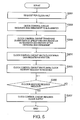
- FIG. 5 illustrates a flowchart in the case of halting the clock in the information processing unit according to the second embodiment of the present invention.
- the clock control circuit 3 Upon receiving the clock halt request, the clock control circuit 3 asserts a bus request signal (BUSREQ0) in order to obtain bus ownership (S202). A request for bus ownership is made to the arbiter 2 through this bus request signal (BUSREQ0). The arbiter 2 asserts a bus grant signal (GRANT0) to the clock control circuit 3 since the highest priority in the arbitration priority ranking is assigned to the clock control circuit 3.
- BUSREQ0 bus request signal
- GRANT0 bus grant signal
- the clock control circuit 3 becomes the bus master after the bus grant signal (GRANT0) is asserted.
- the address phase the address of the clock halt trigger register in the clock control circuit 3 is output to the system bus 12 as the transfer destination address.
- the clock control circuit 3 outputs dummy data (S203).
- the clock control circuit 3 halts the clock when the clock halt trigger register in the clock control circuit 3 is written into through this bus transaction (S204).
- the clock control circuit 3 stays in the wait state until an instruction to return to normal operation, or a clock restore request is received (S205). If there is an instruction to return to normal operation following the clock halt (S206), the clock control circuit 3 resumes clock supply (S207). It should be noted that because there is no suspended data transfer when the clock is halted since the clock control circuit 3 becomes the bus master and halts the clock, it is not necessary for it to become the bus master when resuming clock supply.
- a third embodiment of the present invention relates to an information processing unit that has an oscillator clock supplied to the system bus and peripheral processors that merely passes through the PLL during the PLL lock-up period.
- the fundamental configuration of this information processing unit is same as that of the first embodiment of the present invention.
- a clock generated by multiplying the clock of the oscillator 7 with the clock multiplying PLL 6 is supplied to the CPU 1 and peripheral processors 10 and 11.
- the clock multiplying PLL 6 is turned off (OFF) in order to reduce the clock multiplying PLL 6 power consumption.
- the clock of the oscillator 7 is supplied to the system bus 12 and peripheral processors 10 and 11 merely passes through the PLL.
- the clock multiplied by the clock multiplying PLL 6 is switched to be clock output to the CPU 1 and peripheral processors 10 and 11.
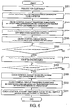
- FIG. 6 is a flowchart illustrating the processing operation of an information processing unit according to a third embodiment of the invention.
- the clock control circuit 3 Upon receiving the clock halt request, the clock control circuit 3 asserts a bus request signal (BUSREQ0) in order to obtain bus ownership (S302). Bus ownership is requested to the arbiter 2 by this bus request signal (BUSREQ0).
- the arbiter 2 asserts a bus grant signal (GRANT0) to the clock control circuit 3 since the highest priority in the arbitration priority ranking is assigned to the clock control circuit 3.
- the clock control circuit 3 becomes the bus master after the bus grant signal (GRANT0) is asserted.
- the address phase the address of the clock halt trigger register in the clock control circuit 3 is output to the system bus 12 as a transfer destination address.
- the clock control circuit 3 outputs dummy data (S303).
- the clock control circuit 3 stays in the wait state until an instruction to return to normal operation, or a clock restore request is received (S305). If there is an instruction to return to normal operation after halting the clock (S306), the clock control circuit 3 turns the clock multiplying PLL 6 on, and until the PLL enters locked state or the phase is synchronized, the clock from the oscillator 7 merely passes through the PLL and is supplied to the CPU 1 and peripheral processors 10 and 11 (S307).
- the clock control circuit 3 makes a request for bus ownership of the system bus 12 to the arbiter 2 (S309). Namely, the clock control circuit 3 asserts the bus request signal (BUSREQ0) to the arbiter 2.
- BUSREQ0 bus request signal
- the arbiter 2 asserts the bus grant signal (GRANT0) to the clock control circuit 3.
- the clock control circuit 3 becomes the bus master after the bus grant signal (GRANT0) is asserted.
- the address phase the address of the clock halt trigger register in the clock control circuit 3 is output to the system bus 12 as the transfer destination address.
- the clock control circuit 3 outputs dummy data (S310).
- the clock control circuit 3 switches from a clock supplied to the CPU 1 and peripheral processors 10 and 11 from the direct output of the clock of the oscillator 7, to the clock output that has been multiplied by the clock multiplying PLL 6 when the clock halt trigger register in the clock control circuit 3 is written through this bus transaction (S311).
- a fourth embodiment of the present invention relates to an information processing unit that performs writing in the clock switch or clock halt trigger register from a device other than the clock control circuit, such as the CPU or peripheral processor.
- the fundamental configuration of this information processing unit is same as that of the first embodiment of the present invention.
- the clock control circuit in the case where the clock control circuit receives a request for a clock switch or clock halt, it was the clock control circuit itself that was performing the dummy data transfer to write into the clock switch trigger register. Nevertheless, when writing into the clock switch trigger register, the contents of the dummy data output to the system bus have no meaning. Since there is no problem if this data is lost due to a clock switch, it is not necessary to limit the bus master that writes into the clock switch trigger register to only the clock control circuit.
- the CPU or peripheral processor itself may become the bus master to directly write into the clock switch trigger register in the clock control circuit without generating a clock switch request signal.
- the clock control circuit switches the clock timed with when the trigger register is written. Since it may be determined that no data transfer is being performed on the system bus when the clock switch trigger register is written, it is possible to switch the clock at a time where data transfer is not performed on the system bus.
- the peripheral processor when the arbitration priority of the peripheral processor is low, the peripheral processor is kept waiting until it becomes the bus master. Accordingly, by assigning an arbitration priority ranking to the peripheral processor having the trigger register writing function that is higher than that of the peripheral processor that has no need for writing into the trigger register, the former becomes the bus master immediately and can switch the clock by writing into the clock switch trigger register.
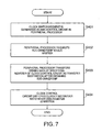
- FIG. 7 is a flowchart illustrating the processing operation of an information processing unit according to a fourth embodiment of the present invention.
- the peripheral processor 10 asserts a bus request signal (BUSREQ0) in order to obtain bus ownership.
- a request for bus ownership is made to the arbiter 2 by this bus request signal (BUSREQ0) (S402).
- the arbiter 2 asserts a bus grant signal (GRANT0) to the peripheral processor 10.
- the peripheral processor 10 becomes the bus master after the bus grant signal (GRANT0) is asserted.
- the peripheral processor 10 outputs the address of the clock switch trigger register in the clock control circuit 3 to the system bus 12 as the transfer destination address.
- the peripheral processor 10 outputs dummy data (S403).
- the clock control circuit 3 switches the clock frequency division ratio when the clock switch trigger register in the clock control circuit 3 is written through this bus transaction (S404). In this manner, it is possible to perform a clock switch.
Landscapes
- Engineering & Computer Science (AREA)
- Theoretical Computer Science (AREA)
- Physics & Mathematics (AREA)
- General Engineering & Computer Science (AREA)
- General Physics & Mathematics (AREA)
- Bus Control (AREA)
- Power Sources (AREA)
- Information Transfer Systems (AREA)
Abstract
Description
Claims (7)
- An information processing unit having a system bus that connects devices configuring an information processing unit; an arbiter that performs arbitration related to use of this system bus; and a clock control circuit that controls a clock to be supplied to the devices,
wherein the clock control circuit comprises: means for performing a bus request to the arbiter; and means for performing a clock switch or clock halt after being granted use of the bus by the arbiter. - The information processing unit mentioned in Claim 1,
wherein said means for performing a clock switch or clock halt, of the clock control circuit comprises:means for transferring prescribed data by specifying a prescribed register as a transfer destination address; andmeans for performing a clock switch or clock halt in response to write-in of prescribed data into the register. - The information processing unit mentioned in Claim 1,
wherein the means for performing clock switch or clock halt of the clock control circuit comprises:means for writing prescribed data into a prescribed register by a device other than the clock control circuit; andmeans for performing a clock switch or clock halt in response to write-in of prescribed data into the register. - The information processing unit mentioned in one of claims 1 to 3 further comprising: an oscillator that outputs a first clock; and a PLL circuit that adjusts the phase of the first clock and outputs a second clock,
wherein in the case of restoring a halted clock, the first clock is used until phase adjustment of the first clock by the PLL circuit is completed; and the second clock is used after the phase adjustment of the first clock is completed. - The information processing unit mentioned in one of claims 1 to 4 further comprising: a power management unit that makes a request for a clock switch or clock halt to the clock control circuit in accordance with the presence of a data transfer between memory and peripheral equipment without going through the central processing unit and the transfer speed required for that data transfer.
- The information processing unit mentioned in one of claims 1 to 5 further comprising a bus interface for adjusting data/ address signal transfer between a local bus and a peripheral bus;
wherein the devices include at least a central processing unit and a peripheral processor, the central processing unit is connected to the local bus, and the peripheral processor is connected to the peripheral bus. - An information processing unit which has a system bus that connects devices configuring an information processing unit; an arbiter that performs arbitration related to use of this system bus; and a clock control circuit that controls a clock to be supplied to the devices; comprising:means for performing a bus request to the arbiter from a device other than the clock control circuit; means for writing prescribed data into a prescribed register by a device to which bus grant is given; and means for performing a clock switch or clock halt in response to write-in of the prescribed data into the register.
Applications Claiming Priority (2)
| Application Number | Priority Date | Filing Date | Title |
|---|---|---|---|
| JP2002040869A JP3665030B2 (en) | 2002-02-19 | 2002-02-19 | Bus control method and information processing apparatus |
| JP2002040869 | 2002-02-19 |
Publications (2)
| Publication Number | Publication Date |
|---|---|
| EP1345109A2 true EP1345109A2 (en) | 2003-09-17 |
| EP1345109A3 EP1345109A3 (en) | 2006-02-22 |
Family
ID=27678325
Family Applications (1)
| Application Number | Title | Priority Date | Filing Date |
|---|---|---|---|
| EP03003694A Withdrawn EP1345109A3 (en) | 2002-02-19 | 2003-02-18 | Information processing unit |
Country Status (4)
| Country | Link |
|---|---|
| US (1) | US7155631B2 (en) |
| EP (1) | EP1345109A3 (en) |
| JP (1) | JP3665030B2 (en) |
| KR (1) | KR100573942B1 (en) |
Families Citing this family (15)
| Publication number | Priority date | Publication date | Assignee | Title |
|---|---|---|---|---|
| US7302508B2 (en) * | 2003-06-10 | 2007-11-27 | Via Technologies, Inc. | Apparatus and method for high speed data transfer |
| JP4860104B2 (en) * | 2003-10-09 | 2012-01-25 | 日本電気株式会社 | Information processing device |
| US7321979B2 (en) | 2004-01-22 | 2008-01-22 | International Business Machines Corporation | Method and apparatus to change the operating frequency of system core logic to maximize system memory bandwidth |
| FI20040418A7 (en) * | 2004-03-18 | 2005-09-19 | Nokia Corp | Digital system clock control |
| JP4792766B2 (en) * | 2005-02-25 | 2011-10-12 | カシオ計算機株式会社 | Data transfer device and imaging device |
| JP4716167B2 (en) * | 2005-03-28 | 2011-07-06 | 富士ゼロックス株式会社 | Data processing method, data processing apparatus, and image forming apparatus |
| EP1894114B1 (en) * | 2005-06-10 | 2014-08-13 | Freescale Semiconductor, Inc. | Device and method for media access control |
| EP1894116A1 (en) * | 2005-06-10 | 2008-03-05 | Freescale Semiconductor, Inc. | Method and device for frame synchronization |
| US7725759B2 (en) * | 2005-06-29 | 2010-05-25 | Sigmatel, Inc. | System and method of managing clock speed in an electronic device |
| US7467245B2 (en) * | 2005-07-22 | 2008-12-16 | Cisco Technology, Inc. | PCI arbiter |
| US7809973B2 (en) * | 2005-11-16 | 2010-10-05 | Cypress Semiconductor Corporation | Spread spectrum clock for USB |
| JP4846486B2 (en) * | 2006-08-18 | 2011-12-28 | 富士通株式会社 | Information processing apparatus and control method thereof |
| JP2008059047A (en) * | 2006-08-29 | 2008-03-13 | Oki Electric Ind Co Ltd | Information processing system and control method therefor |
| JP5561374B2 (en) | 2010-11-15 | 2014-07-30 | 富士通株式会社 | Information processing system |
| US9841804B2 (en) * | 2012-02-22 | 2017-12-12 | Silicon Laboratories Inc. | Clocking a processor |
Family Cites Families (12)
| Publication number | Priority date | Publication date | Assignee | Title |
|---|---|---|---|---|
| US5914953A (en) * | 1992-12-17 | 1999-06-22 | Tandem Computers, Inc. | Network message routing using routing table information and supplemental enable information for deadlock prevention |
| US5600839A (en) * | 1993-10-01 | 1997-02-04 | Advanced Micro Devices, Inc. | System and method for controlling assertion of a peripheral bus clock signal through a slave device |
| US6163848A (en) * | 1993-09-22 | 2000-12-19 | Advanced Micro Devices, Inc. | System and method for re-starting a peripheral bus clock signal and requesting mastership of a peripheral bus |
| EP0644475B1 (en) | 1993-09-22 | 2004-07-21 | Advanced Micro Devices, Inc. | Apparatus and method for controlling a peripheral bus clock signal |
| DE19706496A1 (en) * | 1997-02-19 | 1998-08-27 | Siemens Ag | Clock supply system for a microcomputer system |
| JP2000020462A (en) | 1998-06-30 | 2000-01-21 | Toshiba Corp | Bus system applied to computer system |
| US6279058B1 (en) * | 1998-07-02 | 2001-08-21 | Advanced Micro Devices, Inc. | Master isochronous clock structure having a clock controller coupling to a CPU and two data buses |
| JP2000276436A (en) | 1999-03-29 | 2000-10-06 | Minolta Co Ltd | Dma control device |
| JP2001051747A (en) | 1999-08-12 | 2001-02-23 | Fujitsu Ltd | Clock control circuit |
| US6496938B1 (en) * | 2000-02-11 | 2002-12-17 | Compaq Information Technologies Group Lp | Enhanced PCI clock control architecture |
| JP2002007316A (en) | 2000-06-19 | 2002-01-11 | Niigata Fuji Xerox Manufacturing Co Ltd | Low power consumption computer system |
| JP3906015B2 (en) * | 2000-07-12 | 2007-04-18 | 株式会社東芝 | LSI having clock frequency switching function, computer system, and clock frequency switching method |
-
2002
- 2002-02-19 JP JP2002040869A patent/JP3665030B2/en not_active Expired - Fee Related
-
2003
- 2003-02-18 EP EP03003694A patent/EP1345109A3/en not_active Withdrawn
- 2003-02-19 KR KR1020030010433A patent/KR100573942B1/en not_active Expired - Fee Related
- 2003-02-19 US US10/367,758 patent/US7155631B2/en not_active Expired - Fee Related
Also Published As
| Publication number | Publication date |
|---|---|
| KR20030069851A (en) | 2003-08-27 |
| US7155631B2 (en) | 2006-12-26 |
| US20030159080A1 (en) | 2003-08-21 |
| KR100573942B1 (en) | 2006-04-26 |
| EP1345109A3 (en) | 2006-02-22 |
| JP2003242104A (en) | 2003-08-29 |
| JP3665030B2 (en) | 2005-06-29 |
Similar Documents
| Publication | Publication Date | Title |
|---|---|---|
| KR100329344B1 (en) | Power management apparatus and method | |
| JP3526920B2 (en) | Computer system and system and method for controlling peripheral bus clock signals | |
| US7155631B2 (en) | Information processing unit with a clock control circuit having access to the system bus during system clock changes | |
| US7752373B2 (en) | System and method for controlling memory operations | |
| US5625807A (en) | System and method for enabling and disabling a clock run function to control a peripheral bus clock signal | |
| EP0679982B1 (en) | System for controlling a peripheral bus clock signal | |
| US10055369B1 (en) | Systems and methods for coalescing interrupts | |
| KR20040091705A (en) | Low power system and method for a data processing system | |
| US6948017B2 (en) | Method and apparatus having dynamically scalable clock domains for selectively interconnecting subsystems on a synchronous bus | |
| JP3552213B2 (en) | SD memory card host controller and clock control method | |
| CN113093899B (en) | Cross-power domain data transmission method | |
| KR100591524B1 (en) | Slave device capable of dynamic clock gating under bus structure and its operation method | |
| US7277976B2 (en) | Multilayer system and clock control method | |
| TWI291624B (en) | Method and device for transferring data and data transfer bridge | |
| US20150177816A1 (en) | Semiconductor integrated circuit apparatus | |
| JP2006040276A (en) | Bus arbitration system and method for reducing power consumption based on selective clock control | |
| EP2109029B1 (en) | Apparatus and method for address bus power control | |
| EP0644475A2 (en) | Apparatus and method for controlling a peripheral bus clock signal | |
| US8645602B2 (en) | Microcomputer | |
| JP4124579B2 (en) | Bus control system | |
| JP3914404B2 (en) | Power saving interface device and power saving method | |
| JPH10133766A (en) | Adaptive power-down clock control | |
| US20060206644A1 (en) | Method of hot switching data transfer rate on bus | |
| JP4649926B2 (en) | Data processing device | |
| EP1712979A1 (en) | IC architecture |
Legal Events
| Date | Code | Title | Description |
|---|---|---|---|
| PUAI | Public reference made under article 153(3) epc to a published international application that has entered the european phase |
Free format text: ORIGINAL CODE: 0009012 |
|
| AK | Designated contracting states |
Kind code of ref document: A2 Designated state(s): AT BE BG CH CY CZ DE DK EE ES FI FR GB GR HU IE IT LI LU MC NL PT SE SI SK TR |
|
| AX | Request for extension of the european patent |
Extension state: AL LT LV MK RO |
|
| PUAL | Search report despatched |
Free format text: ORIGINAL CODE: 0009013 |
|
| AK | Designated contracting states |
Kind code of ref document: A3 Designated state(s): AT BE BG CH CY CZ DE DK EE ES FI FR GB GR HU IE IT LI LU MC NL PT SE SI SK TR |
|
| AX | Request for extension of the european patent |
Extension state: AL LT LV MK RO |
|
| 17P | Request for examination filed |
Effective date: 20060330 |
|
| AKX | Designation fees paid |
Designated state(s): DE FR GB |
|
| STAA | Information on the status of an ep patent application or granted ep patent |
Free format text: STATUS: THE APPLICATION IS DEEMED TO BE WITHDRAWN |
|
| 18D | Application deemed to be withdrawn |
Effective date: 20061003 |