EP1345052A2 - Re-connectable optical interface system and method for optically interconnecting and disconnecting optical devices - Google Patents
Re-connectable optical interface system and method for optically interconnecting and disconnecting optical devices Download PDFInfo
- Publication number
- EP1345052A2 EP1345052A2 EP02023241A EP02023241A EP1345052A2 EP 1345052 A2 EP1345052 A2 EP 1345052A2 EP 02023241 A EP02023241 A EP 02023241A EP 02023241 A EP02023241 A EP 02023241A EP 1345052 A2 EP1345052 A2 EP 1345052A2
- Authority
- EP
- European Patent Office
- Prior art keywords
- optical
- insert
- waveguides
- optically
- beamsplitter
- Prior art date
- Legal status (The legal status is an assumption and is not a legal conclusion. Google has not performed a legal analysis and makes no representation as to the accuracy of the status listed.)
- Granted
Links
Images




Classifications
-
- G—PHYSICS
- G02—OPTICS
- G02B—OPTICAL ELEMENTS, SYSTEMS OR APPARATUS
- G02B6/00—Light guides; Structural details of arrangements comprising light guides and other optical elements, e.g. couplings
- G02B6/24—Coupling light guides
- G02B6/26—Optical coupling means
- G02B6/35—Optical coupling means having switching means
- G02B6/351—Optical coupling means having switching means involving stationary waveguides with moving interposed optical elements
- G02B6/3512—Optical coupling means having switching means involving stationary waveguides with moving interposed optical elements the optical element being reflective, e.g. mirror
-
- G—PHYSICS
- G02—OPTICS
- G02B—OPTICAL ELEMENTS, SYSTEMS OR APPARATUS
- G02B6/00—Light guides; Structural details of arrangements comprising light guides and other optical elements, e.g. couplings
- G02B6/24—Coupling light guides
- G02B6/26—Optical coupling means
- G02B6/28—Optical coupling means having data bus means, i.e. plural waveguides interconnected and providing an inherently bidirectional system by mixing and splitting signals
- G02B6/2804—Optical coupling means having data bus means, i.e. plural waveguides interconnected and providing an inherently bidirectional system by mixing and splitting signals forming multipart couplers without wavelength selective elements, e.g. "T" couplers, star couplers
- G02B6/2817—Optical coupling means having data bus means, i.e. plural waveguides interconnected and providing an inherently bidirectional system by mixing and splitting signals forming multipart couplers without wavelength selective elements, e.g. "T" couplers, star couplers using reflective elements to split or combine optical signals
-
- G—PHYSICS
- G02—OPTICS
- G02B—OPTICAL ELEMENTS, SYSTEMS OR APPARATUS
- G02B6/00—Light guides; Structural details of arrangements comprising light guides and other optical elements, e.g. couplings
- G02B6/24—Coupling light guides
- G02B6/42—Coupling light guides with opto-electronic elements
- G02B6/43—Arrangements comprising a plurality of opto-electronic elements and associated optical interconnections
Definitions
- PCBs printed circuit boards
- various electronic components such as resistors, diodes, integrated circuits (IC) and central processing units (CPUs)
- PCBs include prefabricated circuits, which are known as "conductor patterns," that provide electrical connections between the electronic components mounted on the PCBs.
- conductor patterns that provide electrical connections between the electronic components mounted on the PCBs.
- PCBs may be used in more than one application. Consequently, PCBs can be customized by mounting different electronic components on the PCB.
- Electronic components may be mounted on a PCB by soldering the components onto the PCB.
- the conductor patterns are fabricated on one side of the PCB and the electronic components are mounted on the opposite side.
- the electronic components suitable for mounting on PCBs typically include electrically conductive pins that protrude in one direction.
- the electronic components are mounted on the PCB by inserting the pins of the electronic components through the PCB and then soldering the pins to the conductor patterns.
- the mounted electronic components are electrically connected to the conductor patterns of the PCB.
- the soldering of electronic components to the conductor patterns of a PCB provides an effective method to mount the components onto the PCB and to electrically connect the components to the PCB. However, the soldering method does not allow the mounted electronic components to be easily removed from the PCB.
- some PCBs include sockets that are attached to the PCBs and connected to the respective conductor patterns.
- the sockets are receptacles into which pins of electronic components can be inserted to mount the components to the PCBs.
- An example of a socket is a Zero Insertion Force (ZIF) socket, which is commonly used to mount a CPU onto a PCB.
- ZIF Zero Insertion Force
- the electronic component can then be easily removed from the PCB by pulling out the pins of the component from the socket.
- the electronic component can be remounted to the original PCB or mounted to a different PCB by inserting the pins of the component into the respective socket.
- OCBs optical circuit boards
- OCBs can be viewed as the optical equivalents of PCBs. Similar to the conductor patterns on PCBs, OCBs include waveguides that can be optically connected to various optical components to optically interconnect the optical components.
- an optical component is optically connected to an OCB by physically attaching one or more waveguides of the component to the desired waveguides of the OCB by using an adhesive material, such as epoxy.
- an optical component is optically connected to an OCB by mechanically abutting polished ends of waveguides, and then fixing the waveguides in place.
- a concern with these prior art methods to optically connect optical components to OCBs is that the optical components cannot be easily connected to and disconnected from the OCBs.
- a re-connectable optical interface system and method for optically interconnecting and disconnecting optical devices utilizes an optical insert with a reflective element and an optical structure with a displaceable optically bridging element, which can be positioned between two waveguides of the optical structure, to optically connect the optical devices.
- the optical insert is a part of a first optical device, while the optical structure is a part of a second optical device.
- the optical insert and the optical structure can be interconnected to establish an optical connection between the optical insert of the first optical device and at least one of the waveguides of the second optical device.
- the optically bridging element is positioned between the waveguides to provide an optical connection between the waveguides.
- a re-connectable optical interface system in accordance with the invention includes an optical structure and an optical insert.
- the optical structure includes first and second waveguides, which are separated by an opening.
- the optical insert includes a reflective element, which can be optically aligned with at least one of the first and second waveguides when the optical insert is inserted into the opening of the optical structure.
- the reflective element of the optical insert includes a mirror or a facet configured to cause total reflection for incident optical signals when the optical insert is inserted into the optical structure.
- the reflective element includes a beamsplitter configured to partially reflect incident optical signals when the optical insert is inserted into the optical structure.
- the optical insert may include a mirror positioned to reflect incident optical signals toward the beamsplitter.
- the reflective element includes a polarizing beamsplitter configured to selectively reflect particular polarization components of when the optical insert is inserted into the optical structure.
- the optical insert may include an optical element and a mirror.
- the optical element may include an electrically controllable birefringent material, which may be configurable as a quarter-wave plate.
- the optical structure includes a bridging element configured to establish an optical connection between the first and second waveguides when the bridging element is placed in an optically aligned position in the opening of the optical structure.
- the optical structure may include a displacing mechanism configured to position the bridging element to the optically aligned position when no external force is applied, and to permit displacement of the bridging element from the optically aligned position when an external force is applied.
- a method for optically interfacing optical devices in accordance with the invention includes the step of providing a first optical device and the step of providing a second optical device.
- the first optical device includes an optical insert with a reflective element.
- the second optical device includes first and second waveguides that are separated by an opening.
- the method further includes the step of inserting the optical insert of the first optical device into the opening of the second optical device, including aligning the reflective element of the optical insert with at least one of the first and second waveguides to establish a new optical connection between the optical insert and one of the optically aligned waveguides.
- the method may include the step of displacing a bridging element of the optical structure from the opening.
- the bridging element is configured to establish an optical connection between the first and second waveguides when the bridging element is positioned in the opening.
- the method may further include the step of removing the optical insert from the opening, including positioning the bridging element back in the opening to re-establish the optical connection between the first and second waveguides through the bridging element.
- the step of inserting the optical insert into the opening includes aligning a beamsplitter of the optical insert, which is configured to partially reflect incident optical signals, with at least one of the first and second waveguides.
- the step of inserting the optical insert into the opening includes aligning a polarizing beamsplitter of the optical insert, which is configured to selectively reflect particular polarization components of incident light signals, with at least one of the first and second waveguides.
- Fig. 2 is a cross-sectional view of the re-connectable optical interface system of Fig. 1 when the optical insert and the optical structure of the system are interconnected.
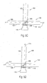
- Figs. 3A-3C are diagrams of optical signal paths through the re-connectable optical interface system of Fig. 1.
- Fig. 4 is a cross-sectional view of a re-connectable optical interface system in accordance with a second embodiment of the present invention.
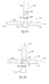
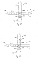
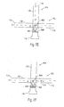
- Figs. 5A-5D are diagrams of optical signal paths through the re-connectable optical interface system of Fig. 4.
- Fig. 6 is a cross-sectional view of a re-connectable optical interface system in accordance with a third embodiment of the present invention.
- Figs. 7A-7E are diagrams of optical signal paths through the re-connectable optical interface system of Fig. 6.
- Fig. 8 is a cross-sectional view of the re-connectable optical interface system of Fig. 6 in accordance with an alternative configuration.
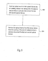
- Fig. 9 is a flow diagram of a method for optically interconnecting and disconnecting optical devices in accordance with an embodiment of the present invention.
- the re-connectable optical interface system includes an optical structure 102 and an optical insert 104 that can be interconnected to establish an optical connection between the optical structure and the optical insert.
- the configurations of the optical structure and the optical insert are such that the optical insert can be repeatedly connected to and disconnected from the optical structure.
- the re-connectable optical interface system provides a desirable means to establish and terminate optical connections between optical devices that embody the re-connectable optical interface system.
- the re-connectable optical interface system may be used to connect an optical component to an optical circuit board (OCB).
- the optical insert may be a part of the optical component, while the optical structure may be a part of the OCB.
- the optical component is optically connected to the OCB.
- the optical structure 102 of the re-connectable optical interface system 100 includes a substrate 106, waveguides 108 and 110, and aligners 112.
- the substrate 106 can be made of any material that is commonly used in optical circuits.
- the waveguides 108 and 110 of the optical structure are positioned on the substrate such that an opening 114 exists between the two waveguides.
- the opening between the waveguides may be created by forming a via through a single waveguide, which will result in the two waveguides 108 and 110.
- the aligners 112 of the optical structure are located above the waveguides. The aligners are designed to properly position the optical insert 104 when the optical insert is being connected with the optical structure.
- the optical structure 102 further includes an optically bridging element 116 and a displacing mechanism 118.
- the optically bridging element is a plug that can be positioned in the opening 114 between the waveguides 108 and 110, as illustrated in Fig. 1. Consequently, the optically bridging element has a circular shape to fit in the opening. Furthermore, the optically bridging element has an index of refraction profile that matches the index of refraction profile of the waveguides. Thus, when the optically bridging element is positioned in the opening, an optical connection is established between the waveguides through the optically bridging element.
- the displacing mechanism 118 of the optical structure 102 operates to position the optically bridging element 114 within the opening between the waveguides 108 and 110 when no external force is applied to the optically bridging element so that the waveguides are optically connected. However, when a downward pressure is applied to the optically bridging element, the displacing mechanism is configured to yield to the downward pressure, allowing the optically bridging element to be lowered. The downward displacement of the optically bridging element terminates the optical connection between the waveguides through the optically bridging element.
- the displacing mechanism may be any type of mechanism that is configured to yield to a downward pressure and to return to its original state when the downward pressure is removed.
- the displacing mechanism may be a spring with sufficient tension to hold the optically bridging element in the optically aligned position within the opening when no downward pressure is applied to the optically bridging element. However, when a downward pressure is applied, the spring has sufficient give to allow the optically bridging element to be lowered out of the optically aligned position.
- the optical insert 104 of the re-connectable optical interface system 100 is an optically conductive pin that is designed to be inserted into the opening 114 of the optical structure 102 to optically interface with the waveguide 108 and 110, as illustrated in Fig. 2.
- the optical insert 104 When the optical insert 104 is being inserted into the opening 114, the optical insert exerts a downward pressure on the optically bridging element 116, which results in a downward displacement of the optically bridging element.
- the optical connection between the waveguides through the optically bridging element is terminated when the optical insert is inserted into the opening.
- the optically bridging element is raised back to the optically aligned position to re-establish the optical connection between the waveguides through the optically bridging element.
- the optical insert 104 includes an optically conductive region 120, an optional lens 121, a reflective element 122 and aligners 124.
- the optically conductive region 120 is made of a transparent material, such as silica.
- the optically conductive region of the optical insert functions as a waveguide for transmission of optical signals through the optical insert.
- the optional lens 121 can be included in the optical insert to focus or collimate beams of light propagating through the optical insert.
- the reflective element 122 of the optical insert is located at the end of the optical insert.
- the aligners 124 ofthe optical insert are located on the periphery of the optical insert to engage the aligners 112 of the optical structure 102 as the optical insert is being inserted into the opening 114 of the optical structure.
- the re-connectable optical interface system 100 includes an interlock mechanism to hold the optical insert 104 in place when the optical insert is inserted into the opening 114 of the optical structure 102 to interconnect the optical insert and the optical structure.
- the interlock mechanism is configured to be disengaged when the optical insert needs to be disconnected from the optical structure.
- Figs. 3A, 3B and 3C illustrate paths of optical signals through the optical insert 104 and the optical structure 102 of the system.
- Fig. 3A illustrates the path of optical signals when the optical insert and the optical structure are not interconnected
- Figs. 3B and 3C illustrate the paths of optical signals when the optical insert and the optical structure are interconnected.
- Fig. 3A illustrates the path of optical signals when the optical insert and the optical structure are not interconnected
- Figs. 3B and 3C illustrate the paths of optical signals when the optical insert and the optical structure are interconnected.
- optical signals from the waveguide 108 are reflected downward off the reflective element and are transmitted toward the substrate of the optical structure, where the optical signals are lost, as illustrated by a path 306 in Fig. 3C.
- the waveguide 108 is not connected to either the optical insert or the waveguide 110.
- the optical insert 404 of the re-connectable optical interface system 400 includes the optically conductive region 120, the optional lens 121, a beamsplitter 406, a mirror 408 and the aligners 124.
- the beamsplitter 406 is orientated at approximately forty-five degrees to partially reflect a propagating light beam such that half of the light beam is perpendicularly reflected, while the other half of the light beam is transmitted through the beamsplitter without change in direction.
- the beamsplitter may include a silver mirror orientated at a forty-five degree angle that is configured to divide an input light beam into two perpendicularly propagating light beams, each light beam having half the intensity of the input light beam.
- the beamsplitter operates to partially reflect a horizontally propagating light beam that impinges the beamsplitter from the left in an upward direction, and to partially reflect a horizontally propagating light beam that impinges the beamsplitter from the right in a downward direction.
- the beamsplitter operates to partially reflect a vertically propagating light beam that impinges the beamsplitter from above in a horizontal direction to the left, and to partially reflect a vertically propagating light beam that impinges the beamsplitter from the right in a horizontal direction to the right.
- a bi-directional optical connection is established between the waveguides through the optically bridging element 116, as illustrate by an optical path 502 in Fig. 5A.
- input optical signals from the waveguide 108 are transmitted to the waveguide 110 through the optically bridging element along the optical path 502.
- input optical signals from the waveguide 110 are transmitted to the waveguide 108 through the optically bridging element along the same optical path.
- the bi-directional optical connection between the waveguides 108 and 110 through the optically bridging element 116 is terminated due to the displacement of the optically bridging element by the optical insert.
- new optical connections between the optical insert and the waveguides are established, as illustrated in Figs. 5B, 5C and 5D.
- the new optical connections include optical connections from the waveguide 108 to the optical insert and the waveguide 110, as illustrated in Fig. 5B.
- input optical signals from the waveguide 108 are partially reflected by the beamsplitter 406 of the optical insert such that reflected portions of the optical signals are transmitted upward along the optical insert and non-reflected portions of the optical signals are transmitted to the waveguide 110 through the optical insert, as illustrated by optical paths 504 and 506, respectively.
- the new optical connections established by the interconnection of the optical insert 404 and the optical structure 102 include optical connections from the optical insert to the waveguides 108 and 110, as illustrated in Fig. 5C.
- input optical signals from the optical insert are partially reflected by the beamsplitter 406 of the optical insert such that reflected portions of the optical signals are transmitted to the waveguide 108, as illustrated by an optical path 508.
- the non-reflected portions of the optical signals are transmitted downward toward the mirror 408 of the optical insert through the beamsplitter.
- the non-reflected portions of the optical signals are then reflected off the mirror and transmitted back to the beamsplitter.
- these portions of the optical signals are further partially reflected and transmitted to the waveguide 110, as illustrated by an optical path 510.
- the non-reflected portions of the optical signals are transmitted back through the optical insert (not illustrated).
- the new optical connections established by the interconnection of the optical insert 404 and the optical structure 102 include optical connections from the waveguide 110 to the optical insert and the waveguide 108, as illustrated in Fig. 5D.
- input optical signals from the waveguide 110 are partially reflected by the beamsplitter 406 of the optical insert such that non-reflected portions of the optical signals are transmitted to the waveguide 108 through the beamsplitter, as illustrated by an optical path 512.
- the reflected portions of the optical signals are transmitted toward the mirror 408 of the optical insert.
- the reflected portions of the optical signals are then reflected off the mirror and transmitted back to the beamsplitter.
- these portions of the optical signals are further partially reflected such that non-reflected portions of the optical signals are transmitted to the optical insert, as illustrated by an optical path 514.
- the reflected portions of the optical signals are transmitted back to the waveguide 110 (not illustrated).
- a re-connectable optical interface system 600 in accordance with a third embodiment of the invention is shown.
- the re-connectable optical interface system 600 includes the interlock mechanism (not shown), the optical structure 102 and an optical insert 604. Similar to the optical insert 404 of the re-connectable optical interface system 400 of Fig. 4, the optical insert 604 is designed to establish optical connections between the optical insert and the waveguides 108 and 110, when the optical insert and the optical structure are interconnected.
- the optical insert 604 of the re-connectable optical interface system 600 includes the optically conductive region 120, the optional lens 121, a polarizing beamsplitter 606, an optical element 608, the mirror 408 and the aligners 124.
- the polarizing beamsplitter 606 is orientated at approximately forty-five degrees to reflect only a particular polarization component of an impinging light beam.
- the polarizing beamsplitter is designed to reflect only the S polarization component of a horizontally propagating light beam such that the S polarization component is reflected either upward or downward, while the P polarization component is transmitted through the polarizing beamsplitter without change in direction.
- the S polarization component of a light beam that impinges upon the polarizing beamsplitter from the left is reflected upward and the S polarization component of a light beam that impinges upon the polarizing beamsplitter from the right is reflected downward.
- the polarizing beamsplitter is designed to reflected only the S polarization component of a vertically propagating light beam such that the S polarization component is reflected either horizontally to the left or horizontally to the right, while the P polarization component is transmitted through the polarizing beamsplitter without change in direction.
- the S polarization component of a light beam that impinges upon the polarizing beamsplitter from above is reflected horizontally to the left and the S polarization component of a light beam that impinges upon the polarization beamsplitter from below is reflected horizontally to the right.
- the optical element 608 of the optical insert 604 is positioned between the polarizing beamsplitter 606 and the mirror 408.
- the optical element is a quarter-wave plate that operates to switch the polarization direction of polarization components of optical signals as the polarization components propagate twice through the quarter-wave plate due to the mirror.
- the optical element is a controllable quarter-wave plate.
- the optical element includes a layer of electrically controlled birefringent (ECB) material (not shown), such as a liquid crystal cell or a slab of Lithium Niobate, and electrodes (not shown), which can generate an electric field within the ECB layer.
- the ECB layer can be switched between an active state and an inactive state using an electric field.
- the ECB layer functions as a quarter-wave plate.
- the ECB layer becomes optically passive.
- the ECB layer is configured to switch to the active state when an electric field is applied.
- the ECB layer is configured to switch to the inactive state when an electric field is applied.
- the thickness and orientation of the ECB layer are predefined to provide quarter-wave retardation of a particular direction of polarization for a propagating light beam when the ECB layer is switched to the active state.
- the optical element functions as a quarter-wave plate.
- the optical element becomes optically passive.
- the optical element in conjunction with the mirror 408 operates to switch the polarization directions of S and P polarization components, as described in more detail below.
- the optical element becomes optically passive and allows the S and P polarization components to be reflected from the mirror without changes in polarization directions.
- the bi-directional-optical connection between the waveguides 108 and 110 through the optically bridging element 116 is terminated due to the displacement of the optically bridging element by the optical insert.
- new optical connections between the optical insert and the waveguides are established, as illustrated in Figs. 7B, 7C, 7D, 7E and 7F.
- the new optical connections include optical connections from the waveguide 108 to the optical insert 604 and the waveguide 110, as illustrated in Fig. 7B by optical paths 704 and 706.
- the P polarization components are twice retarded by the optical element.
- the linear P polarization components are converted into circular polarization components by the optical element.
- the circular polarization components are then reflected off the mirror 408, which changes the handedness of the circular polarization components.
- the circular polarization components are converted back to linear polarization components.
- the original P polarization components are converted to S polarization components.
- the new optical connections established by the interconnection of the optical insert 604 and the optical structure 102 further include optical connections from the waveguide 110 to the optical insert and the waveguide 108, as illustrated by optical paths 714, 716 and 718 in Figs. 7E and 7F.
- the optical path 714 in Figs. 7E and 7F illustrates the path of the P polarization components of input optical signals from the waveguide 110, regardless of the optical state of the optical element 608 of the optical insert.
- the optical path 716 in Fig. 7E illustrates the path of the S polarization components of the input signals when the optical element is activated to function as a quarter-wave plate, while the optical path 718 in Fig.
- FIG. 7F illustrates the path of the S polarization components when the optical element is deactivated to a passive state.
- the P polarization components of the input optical signals from waveguide 110 are transmitted through the polarizing beamsplitter 606 without change in direction to the waveguide 108, as shown by the path 714 in Figs. 7E and 7F.
- the S polarization components of the input optical signals are reflected downward by the polarizing beamsplitter 606 to the mirror 408 and are reflected back off the mirror to the polarizing beamsplitter, as illustrated by the paths 716 and 718 in Figs. 7E and 7F, respectively.
- the polarization directions of the returning polarization components again depend on the optical state of the optical element 608.
- the S polarization components are converted to P polarization components by the optical element, as described above in reference to Fig. 7C.
- the converted P polarization components impinge upon the polarizing beamsplitter 606, these polarization components are transmitted through the polarizing beamsplitter to the optical insert without change in direction, as shown by the optical path 716 in Fig. 7E.
- the optical element is deactivated to a passive state, the polarization direction of the S polarization components is not altered by the optical element.
- the S polarization components are reflected off the mirror 408 and impinge upon the polarizing beamsplitter as S polarization components.
- the optical insert of the first optical device is removed from the opening of the second optical device to optically disconnect the first and second optical devices.
- the removal of the optical insert causes the optically bridging element of the second optical device to be positioned back to the opening between the two waveguides to re-establish the optical connection between the waveguides.
- the first optical device can be repeatedly connected to the second optical device.
- one or both of the first and second optical devices may be connected to different optical devices.
Landscapes
- Physics & Mathematics (AREA)
- General Physics & Mathematics (AREA)
- Optics & Photonics (AREA)
- Optical Couplings Of Light Guides (AREA)
- Optical Integrated Circuits (AREA)
Abstract
Description
Claims (10)
- An optical interface system (100; 400; 600) comprising:an optical structure (102) including a first waveguide (108) and a second waveguide (110), said first and second waveguides being separated by an opening (114); andan optical insert (104; 404; 604) including a reflective element (122; 406; 606), said optical insert being configured to be inserted into said opening to establish an optical connection with at least one of said first and second waveguides when said reflective element is optically aligned with said at least one of said first and second waveguides.
- The optical interface system (100; 400; 600) of claim 1, wherein said reflective element (122; 406; 606) includes a beamsplitter (406) configured to partially reflect incident optical signals when said optical insert (104; 404; 604) is inserted into said optical structure (102).
- The optical interface system (100; 400; 600) of claim 2, wherein said reflective element (122; 406; 606) includes a polarizing beamsplitter (606) configured to selectively reflect particular polarization components of incident optical signals when said optical insert (104; 404; 604) is inserted into said optical structure (102).
- The optical interface system (100; 400; 600) of claim 3, wherein said optical insert (104; 404; 604) includes an optical element (608) and a mirror (408), said optical element being positioned between said polarizing beamsplitter (606) and said mirror, said optical element being configured as a quarter-wave plate.
- The optical interface system (100; 400; 600) of one of the preceding claims, wherein said optical structure (102) includes a bridging element (116) configured to establish an optical connection between said first and second waveguides (108, 110) when said bridging element is placed in an optically aligned position in said opening (114).
- A method for optically interfacing optical devices, the method comprising:providing a first optical device including an optical insert (104; 404; 604) comprising a reflective element (122; 406; 606);providing a second optical device including first and second waveguides (108, 110) and an opening (114) therebetween; andinserting (902) said optical insert into said opening, including aligning said reflective element of said optical insert with at least one of said first and second waveguides to establish a new optical connection between said optical insert and said at least one of said first and second waveguides.
- The method of claim 6, wherein: said second optical device additionally includes a bridging element (116) configured to establish an optical connection between said first and second waveguides (108, 110) when said bridging element is positioned in said opening (114); and said method additionally comprises displacing said bridging element from said opening.
- The method of claim 7, additionally comprising removing (904) said optical insert (104; 404; 604) from said opening (114), including positioning said bridging element (116) back in said opening to re-establish said optical connection between said first and second waveguides (108, 110) through said bridging element.
- The method of claim 6, 7 or 8, wherein: said optical insert (104; 404; 604) additionally includes a beamsplitter (406) configured to partially reflect incident optical signals; and said aligning of said reflective element (122; 406; 606) of said optical insert with said at least one of said first and second waveguides (108, 110) includes aligning said beamsplitter with said at least one of said first and second waveguides (108, 110), said beamsplitter being orientated to establish said new optical connection between said optical insert and said at least one of said first and second waveguides when said beamsplitter is optically aligned with said at least one of said first and second waveguides.
- The method of claim 6, 7 or 8, wherein: said optical insert (104; 404; 604) additionally includes a polarizing beamsplitter (606) configured to selectively reflect particular polarization components of incident optical signals; and said aligning of said reflective element (122; 406; 606) with said at least one of said first and second waveguides (108, 110) includes aligning said polarizing beamsplitter with said at least one of said first and second waveguides, said polarizing beamsplitter being orientated to establish said new optical connection between said optical insert and said at least one of said first and second waveguides when said polarizing beamsplitter is optically aligned with said at least one of said first and second waveguides.
Applications Claiming Priority (2)
| Application Number | Priority Date | Filing Date | Title |
|---|---|---|---|
| US10/099,517 US6847765B2 (en) | 2002-03-15 | 2002-03-15 | Re-connectable optical interface system and method for optically interconnecting and disconnecting optical devices |
| US99517 | 2002-03-15 |
Publications (3)
| Publication Number | Publication Date |
|---|---|
| EP1345052A2 true EP1345052A2 (en) | 2003-09-17 |
| EP1345052A3 EP1345052A3 (en) | 2004-03-31 |
| EP1345052B1 EP1345052B1 (en) | 2005-09-07 |
Family
ID=27765449
Family Applications (1)
| Application Number | Title | Priority Date | Filing Date |
|---|---|---|---|
| EP02023241A Expired - Lifetime EP1345052B1 (en) | 2002-03-15 | 2002-10-16 | Re-connectable optical interface system and method for optically interconnecting and disconnecting optical devices |
Country Status (4)
| Country | Link |
|---|---|
| US (1) | US6847765B2 (en) |
| EP (1) | EP1345052B1 (en) |
| JP (1) | JP2003294977A (en) |
| DE (1) | DE60206016T2 (en) |
Cited By (1)
| Publication number | Priority date | Publication date | Assignee | Title |
|---|---|---|---|---|
| EP2521933A4 (en) * | 2010-01-06 | 2013-11-20 | Hewlett Packard Development Co | Optical interconnect |
Families Citing this family (12)
| Publication number | Priority date | Publication date | Assignee | Title |
|---|---|---|---|---|
| US20030128933A1 (en) * | 2002-01-10 | 2003-07-10 | International Business Machines Corporation | Light-coupling device |
| US7082238B2 (en) * | 2002-03-19 | 2006-07-25 | Avago Technologies | Self-aligning optical interconnect utilizing conformal materials |
| JP3887371B2 (en) * | 2003-11-27 | 2007-02-28 | インターナショナル・ビジネス・マシーンズ・コーポレーション | Optical transmission board, optical transmission board manufacturing method, and opto-electric integrated circuit |
| WO2006059510A1 (en) * | 2004-12-02 | 2006-06-08 | Mitsui Chemicals, Inc. | Optical wiring substrate and optical and electric combined substrate |
| JP2009069186A (en) * | 2007-09-10 | 2009-04-02 | Fuji Xerox Co Ltd | Optoelectronic circuit board |
| KR101629531B1 (en) * | 2009-01-07 | 2016-06-10 | 휴렛-팩커드 디벨롭먼트 컴퍼니, 엘.피. | Photonic waveguide |
| JP5089643B2 (en) * | 2009-04-30 | 2012-12-05 | インターナショナル・ビジネス・マシーンズ・コーポレーション | Optical connection element manufacturing method, optical transmission board, optical connection component, connection method, and optical transmission system |
| CN102576130B (en) | 2009-12-21 | 2014-04-09 | 惠普发展公司,有限责任合伙企业 | Circuit switched optical interconnection fabric |
| US9594214B1 (en) * | 2013-03-15 | 2017-03-14 | Wavefront Research, Inc. | Optical fiber devices |
| JP5865302B2 (en) * | 2013-07-01 | 2016-02-17 | 株式会社ユニバーサルエンターテインメント | Game machine |
| JP5865301B2 (en) * | 2013-07-01 | 2016-02-17 | 株式会社ユニバーサルエンターテインメント | Game machine |
| JP6039049B2 (en) * | 2015-12-24 | 2016-12-07 | 株式会社ユニバーサルエンターテインメント | Game machine |
Family Cites Families (11)
| Publication number | Priority date | Publication date | Assignee | Title |
|---|---|---|---|---|
| US4057719A (en) * | 1976-08-27 | 1977-11-08 | The United States Of America As Represented By The Secretary Of The Navy | Fiber optics electro-mechanical light switch |
| JPS57185410A (en) | 1981-05-11 | 1982-11-15 | Kokusai Denshin Denwa Co Ltd <Kdd> | Optical coupler |
| GB9014639D0 (en) | 1990-07-02 | 1990-08-22 | British Telecomm | Optical component packaging |
| JP2976642B2 (en) | 1991-11-07 | 1999-11-10 | 日本電気株式会社 | Optical coupling circuit |
| US5666448A (en) | 1995-09-22 | 1997-09-09 | Rockwell International Corporation | Variable splitting optical coupler |
| DE19616932A1 (en) * | 1996-04-27 | 1997-10-30 | Bosch Gmbh Robert | Optical, beam-splitting component and method for producing a prism support plate for such a component |
| US5699462A (en) * | 1996-06-14 | 1997-12-16 | Hewlett-Packard Company | Total internal reflection optical switches employing thermal activation |
| US5867617A (en) | 1997-05-19 | 1999-02-02 | E-Tek Dynamics, Inc. | High-reliability MXN fiber optic switches |
| DE19838519A1 (en) * | 1998-08-25 | 2000-03-02 | Bosch Gmbh Robert | Optoelectronic printed circuit board, forms multilayer package with transparent layers |
| TW531669B (en) * | 2000-09-15 | 2003-05-11 | Ibm | Optical devices |
| US6678439B2 (en) * | 2001-06-14 | 2004-01-13 | Martin Hoffmann | Wavelength division multiplexing and broadcast optical interconnection apparatus |
-
2002
- 2002-03-15 US US10/099,517 patent/US6847765B2/en not_active Expired - Fee Related
- 2002-10-16 DE DE60206016T patent/DE60206016T2/en not_active Expired - Fee Related
- 2002-10-16 EP EP02023241A patent/EP1345052B1/en not_active Expired - Lifetime
-
2003
- 2003-03-14 JP JP2003069542A patent/JP2003294977A/en active Pending
Cited By (1)
| Publication number | Priority date | Publication date | Assignee | Title |
|---|---|---|---|---|
| EP2521933A4 (en) * | 2010-01-06 | 2013-11-20 | Hewlett Packard Development Co | Optical interconnect |
Also Published As
| Publication number | Publication date |
|---|---|
| EP1345052A3 (en) | 2004-03-31 |
| DE60206016T2 (en) | 2006-06-29 |
| DE60206016D1 (en) | 2005-10-13 |
| US20030174965A1 (en) | 2003-09-18 |
| US6847765B2 (en) | 2005-01-25 |
| JP2003294977A (en) | 2003-10-15 |
| EP1345052B1 (en) | 2005-09-07 |
Similar Documents
| Publication | Publication Date | Title |
|---|---|---|
| EP0537237B1 (en) | Optical system | |
| US20230418004A1 (en) | Multi-fiber interface apparatus for photonic integrated circuit | |
| CA2013455C (en) | Electro-optical multiple connection arrangement | |
| US6847765B2 (en) | Re-connectable optical interface system and method for optically interconnecting and disconnecting optical devices | |
| US7021833B2 (en) | Waveguide based optical coupling of a fiber optic cable and an optoelectronic device | |
| US5940563A (en) | Receptacle optical module | |
| US6843608B2 (en) | Transparent substrate and hinged optical assembly | |
| JP6168171B1 (en) | Optical module | |
| JP4205170B2 (en) | Flexible foil with connector tab | |
| US7062132B2 (en) | Coupler assembly for an optical backplane system | |
| CN100492079C (en) | Optical waveguide module | |
| EP1784669B1 (en) | Optical assembly with optoelectronic device alignment | |
| CA2409081A1 (en) | Mems optical backplane interface | |
| US5539200A (en) | Integrated optoelectronic substrate | |
| JPH1123914A (en) | Fixing structure between optical element and optical fiber | |
| US6860650B2 (en) | Assembly for aligning an optical array with optical fibers | |
| JP2003131080A (en) | Optical module, manufacturing method thereof, and optical transmission device | |
| WO1998014813A1 (en) | Fiber optic array transmitter/receiver based on flexible circuit technology | |
| AU7584000A (en) | Electrical interconnection of planar lightwave circuits | |
| US20030181098A1 (en) | Plug-in connecting element for optoelectrical devices or subassemblies and plug-in connector with two plug-in connecting elements of this type | |
| KR100641050B1 (en) | Optical backplane device with optical connector | |
| JPH0343704A (en) | Structure of connecting part of printed circuit board |
Legal Events
| Date | Code | Title | Description |
|---|---|---|---|
| PUAI | Public reference made under article 153(3) epc to a published international application that has entered the european phase |
Free format text: ORIGINAL CODE: 0009012 |
|
| AK | Designated contracting states |
Kind code of ref document: A2 Designated state(s): AT BE BG CH CY CZ DE DK EE ES FI FR GB GR IE IT LI LU MC NL PT SE SK TR |
|
| AX | Request for extension of the european patent |
Extension state: AL LT LV MK RO SI |
|
| PUAL | Search report despatched |
Free format text: ORIGINAL CODE: 0009013 |
|
| AK | Designated contracting states |
Kind code of ref document: A3 Designated state(s): AT BE BG CH CY CZ DE DK EE ES FI FR GB GR IE IT LI LU MC NL PT SE SK TR |
|
| AX | Request for extension of the european patent |
Extension state: AL LT LV MK RO SI |
|
| 17P | Request for examination filed |
Effective date: 20040830 |
|
| 17Q | First examination report despatched |
Effective date: 20040923 |
|
| AKX | Designation fees paid |
Designated state(s): DE FR GB |
|
| GRAP | Despatch of communication of intention to grant a patent |
Free format text: ORIGINAL CODE: EPIDOSNIGR1 |
|
| RIN1 | Information on inventor provided before grant (corrected) |
Inventor name: NISHIMURA, KEN |
|
| GRAS | Grant fee paid |
Free format text: ORIGINAL CODE: EPIDOSNIGR3 |
|
| GRAA | (expected) grant |
Free format text: ORIGINAL CODE: 0009210 |
|
| AK | Designated contracting states |
Kind code of ref document: B1 Designated state(s): DE FR GB |
|
| REG | Reference to a national code |
Ref country code: GB Ref legal event code: FG4D |
|
| REF | Corresponds to: |
Ref document number: 60206016 Country of ref document: DE Date of ref document: 20051013 Kind code of ref document: P |
|
| ET | Fr: translation filed | ||
| PLBE | No opposition filed within time limit |
Free format text: ORIGINAL CODE: 0009261 |
|
| STAA | Information on the status of an ep patent application or granted ep patent |
Free format text: STATUS: NO OPPOSITION FILED WITHIN TIME LIMIT |
|
| 26N | No opposition filed |
Effective date: 20060608 |
|
| PGFP | Annual fee paid to national office [announced via postgrant information from national office to epo] |
Ref country code: GB Payment date: 20061025 Year of fee payment: 5 |
|
| PGFP | Annual fee paid to national office [announced via postgrant information from national office to epo] |
Ref country code: DE Payment date: 20071130 Year of fee payment: 6 |
|
| GBPC | Gb: european patent ceased through non-payment of renewal fee |
Effective date: 20071016 |
|
| REG | Reference to a national code |
Ref country code: FR Ref legal event code: ST Effective date: 20080630 |
|
| PGFP | Annual fee paid to national office [announced via postgrant information from national office to epo] |
Ref country code: FR Payment date: 20061017 Year of fee payment: 5 |
|
| PG25 | Lapsed in a contracting state [announced via postgrant information from national office to epo] |
Ref country code: GB Free format text: LAPSE BECAUSE OF NON-PAYMENT OF DUE FEES Effective date: 20071016 |
|
| PG25 | Lapsed in a contracting state [announced via postgrant information from national office to epo] |
Ref country code: FR Free format text: LAPSE BECAUSE OF NON-PAYMENT OF DUE FEES Effective date: 20071031 |
|
| PG25 | Lapsed in a contracting state [announced via postgrant information from national office to epo] |
Ref country code: DE Free format text: LAPSE BECAUSE OF NON-PAYMENT OF DUE FEES Effective date: 20090501 |