EP1341232A2 - Semiconductor device and method for fabricating the same - Google Patents
Semiconductor device and method for fabricating the same Download PDFInfo
- Publication number
- EP1341232A2 EP1341232A2 EP02255356A EP02255356A EP1341232A2 EP 1341232 A2 EP1341232 A2 EP 1341232A2 EP 02255356 A EP02255356 A EP 02255356A EP 02255356 A EP02255356 A EP 02255356A EP 1341232 A2 EP1341232 A2 EP 1341232A2
- Authority
- EP
- European Patent Office
- Prior art keywords
- semiconductor chip
- semiconductor
- fabricating
- semiconductor device
- conductive film
- Prior art date
- Legal status (The legal status is an assumption and is not a legal conclusion. Google has not performed a legal analysis and makes no representation as to the accuracy of the status listed.)
- Withdrawn
Links
Images





Classifications
-
- H—ELECTRICITY
- H10—SEMICONDUCTOR DEVICES; ELECTRIC SOLID-STATE DEVICES NOT OTHERWISE PROVIDED FOR
- H10W—GENERIC PACKAGES, INTERCONNECTIONS, CONNECTORS OR OTHER CONSTRUCTIONAL DETAILS OF DEVICES COVERED BY CLASS H10
- H10W90/00—Package configurations
-
- H—ELECTRICITY
- H10—SEMICONDUCTOR DEVICES; ELECTRIC SOLID-STATE DEVICES NOT OTHERWISE PROVIDED FOR
- H10W—GENERIC PACKAGES, INTERCONNECTIONS, CONNECTORS OR OTHER CONSTRUCTIONAL DETAILS OF DEVICES COVERED BY CLASS H10
- H10W70/00—Package substrates; Interposers; Redistribution layers [RDL]
- H10W70/60—Insulating or insulated package substrates; Interposers; Redistribution layers
-
- H—ELECTRICITY
- H10—SEMICONDUCTOR DEVICES; ELECTRIC SOLID-STATE DEVICES NOT OTHERWISE PROVIDED FOR
- H10W—GENERIC PACKAGES, INTERCONNECTIONS, CONNECTORS OR OTHER CONSTRUCTIONAL DETAILS OF DEVICES COVERED BY CLASS H10
- H10W70/00—Package substrates; Interposers; Redistribution layers [RDL]
- H10W70/01—Manufacture or treatment
- H10W70/05—Manufacture or treatment of insulating or insulated package substrates, or of interposers, or of redistribution layers
- H10W70/093—Connecting or disconnecting other interconnections thereto or therefrom, e.g. connecting bond wires or bumps
-
- H—ELECTRICITY
- H10—SEMICONDUCTOR DEVICES; ELECTRIC SOLID-STATE DEVICES NOT OTHERWISE PROVIDED FOR
- H10W—GENERIC PACKAGES, INTERCONNECTIONS, CONNECTORS OR OTHER CONSTRUCTIONAL DETAILS OF DEVICES COVERED BY CLASS H10
- H10W72/00—Interconnections or connectors in packages
- H10W72/01—Manufacture or treatment
-
- H—ELECTRICITY
- H10—SEMICONDUCTOR DEVICES; ELECTRIC SOLID-STATE DEVICES NOT OTHERWISE PROVIDED FOR
- H10W—GENERIC PACKAGES, INTERCONNECTIONS, CONNECTORS OR OTHER CONSTRUCTIONAL DETAILS OF DEVICES COVERED BY CLASS H10
- H10W72/00—Interconnections or connectors in packages
- H10W72/01—Manufacture or treatment
- H10W72/012—Manufacture or treatment of bump connectors, dummy bumps or thermal bumps
- H10W72/01212—Manufacture or treatment of bump connectors, dummy bumps or thermal bumps at a different location than on the final device, e.g. forming as prepeg
-
- H—ELECTRICITY
- H10—SEMICONDUCTOR DEVICES; ELECTRIC SOLID-STATE DEVICES NOT OTHERWISE PROVIDED FOR
- H10W—GENERIC PACKAGES, INTERCONNECTIONS, CONNECTORS OR OTHER CONSTRUCTIONAL DETAILS OF DEVICES COVERED BY CLASS H10
- H10W72/00—Interconnections or connectors in packages
- H10W72/071—Connecting or disconnecting
- H10W72/072—Connecting or disconnecting of bump connectors
-
- H—ELECTRICITY
- H10—SEMICONDUCTOR DEVICES; ELECTRIC SOLID-STATE DEVICES NOT OTHERWISE PROVIDED FOR
- H10W—GENERIC PACKAGES, INTERCONNECTIONS, CONNECTORS OR OTHER CONSTRUCTIONAL DETAILS OF DEVICES COVERED BY CLASS H10
- H10W72/00—Interconnections or connectors in packages
- H10W72/071—Connecting or disconnecting
- H10W72/073—Connecting or disconnecting of die-attach connectors
-
- H—ELECTRICITY
- H10—SEMICONDUCTOR DEVICES; ELECTRIC SOLID-STATE DEVICES NOT OTHERWISE PROVIDED FOR
- H10W—GENERIC PACKAGES, INTERCONNECTIONS, CONNECTORS OR OTHER CONSTRUCTIONAL DETAILS OF DEVICES COVERED BY CLASS H10
- H10W72/00—Interconnections or connectors in packages
- H10W72/50—Bond wires
- H10W72/551—Materials of bond wires
- H10W72/552—Materials of bond wires comprising metals or metalloids, e.g. silver
- H10W72/5522—Materials of bond wires comprising metals or metalloids, e.g. silver comprising gold [Au]
-
- H—ELECTRICITY
- H10—SEMICONDUCTOR DEVICES; ELECTRIC SOLID-STATE DEVICES NOT OTHERWISE PROVIDED FOR
- H10W—GENERIC PACKAGES, INTERCONNECTIONS, CONNECTORS OR OTHER CONSTRUCTIONAL DETAILS OF DEVICES COVERED BY CLASS H10
- H10W72/00—Interconnections or connectors in packages
- H10W72/851—Dispositions of multiple connectors or interconnections
-
- H—ELECTRICITY
- H10—SEMICONDUCTOR DEVICES; ELECTRIC SOLID-STATE DEVICES NOT OTHERWISE PROVIDED FOR
- H10W—GENERIC PACKAGES, INTERCONNECTIONS, CONNECTORS OR OTHER CONSTRUCTIONAL DETAILS OF DEVICES COVERED BY CLASS H10
- H10W72/00—Interconnections or connectors in packages
- H10W72/90—Bond pads, in general
-
- H—ELECTRICITY
- H10—SEMICONDUCTOR DEVICES; ELECTRIC SOLID-STATE DEVICES NOT OTHERWISE PROVIDED FOR
- H10W—GENERIC PACKAGES, INTERCONNECTIONS, CONNECTORS OR OTHER CONSTRUCTIONAL DETAILS OF DEVICES COVERED BY CLASS H10
- H10W72/00—Interconnections or connectors in packages
- H10W72/90—Bond pads, in general
- H10W72/941—Dispositions of bond pads
- H10W72/9415—Dispositions of bond pads relative to the surface, e.g. recessed, protruding
-
- H—ELECTRICITY
- H10—SEMICONDUCTOR DEVICES; ELECTRIC SOLID-STATE DEVICES NOT OTHERWISE PROVIDED FOR
- H10W—GENERIC PACKAGES, INTERCONNECTIONS, CONNECTORS OR OTHER CONSTRUCTIONAL DETAILS OF DEVICES COVERED BY CLASS H10
- H10W90/00—Package configurations
- H10W90/20—Configurations of stacked chips
- H10W90/22—Configurations of stacked chips the stacked chips being on both top and bottom sides of a package substrate, interposer or RDL
-
- H—ELECTRICITY
- H10—SEMICONDUCTOR DEVICES; ELECTRIC SOLID-STATE DEVICES NOT OTHERWISE PROVIDED FOR
- H10W—GENERIC PACKAGES, INTERCONNECTIONS, CONNECTORS OR OTHER CONSTRUCTIONAL DETAILS OF DEVICES COVERED BY CLASS H10
- H10W90/00—Package configurations
- H10W90/701—Package configurations characterised by the relative positions of pads or connectors relative to package parts
- H10W90/721—Package configurations characterised by the relative positions of pads or connectors relative to package parts of bump connectors
- H10W90/722—Package configurations characterised by the relative positions of pads or connectors relative to package parts of bump connectors between stacked chips
-
- H—ELECTRICITY
- H10—SEMICONDUCTOR DEVICES; ELECTRIC SOLID-STATE DEVICES NOT OTHERWISE PROVIDED FOR
- H10W—GENERIC PACKAGES, INTERCONNECTIONS, CONNECTORS OR OTHER CONSTRUCTIONAL DETAILS OF DEVICES COVERED BY CLASS H10
- H10W90/00—Package configurations
- H10W90/701—Package configurations characterised by the relative positions of pads or connectors relative to package parts
- H10W90/721—Package configurations characterised by the relative positions of pads or connectors relative to package parts of bump connectors
- H10W90/724—Package configurations characterised by the relative positions of pads or connectors relative to package parts of bump connectors between a chip and a stacked insulating package substrate, interposer or RDL
-
- H—ELECTRICITY
- H10—SEMICONDUCTOR DEVICES; ELECTRIC SOLID-STATE DEVICES NOT OTHERWISE PROVIDED FOR
- H10W—GENERIC PACKAGES, INTERCONNECTIONS, CONNECTORS OR OTHER CONSTRUCTIONAL DETAILS OF DEVICES COVERED BY CLASS H10
- H10W90/00—Package configurations
- H10W90/701—Package configurations characterised by the relative positions of pads or connectors relative to package parts
- H10W90/731—Package configurations characterised by the relative positions of pads or connectors relative to package parts of die-attach connectors
- H10W90/732—Package configurations characterised by the relative positions of pads or connectors relative to package parts of die-attach connectors between stacked chips
Definitions
- the present invention relates to a semiconductor device having a layer structure with one semiconductor chip bonded to another, and a method for fabricating the semiconductor device.
- the aforementioned layering method comprises separate steps of forming wires on the semiconductor chip of the wafer and layering another semiconductor chip to be implemented on the semiconductor chip of the wafer.
- these disadvantages conceivably appear when a porous insulating material, the demand for which will grow increasingly, is used as an interlayer insulating film for wires within the semiconductor element.
- the present invention was developed in view of the aforementioned problems. It is desirable to provide a semiconductor device having semiconductor chips stacked in layers and a method for fabricating the semiconductor device.
- a highly reliable semiconductor device provides a simplified manufacturing process and a reduced turnaround time, thereby reducing costs and easily ensuring prevention of breaks in wires and improvement in transmission characteristics.
- the invention is directed to a semiconductor device or package having a composite structure with a first semiconductor chip being bonded to a second semiconductor chip.
- the semiconductor device includes an electrically conductive film layer, portions of which electrically connect the first semiconductor chip and the second semiconductor chip, which layer extends on the element-formed surface of the first semiconductor chip.
- the layer may have been initially formed on a surface having openings so that it is broken into portions corresponding to the openings. Thus, the layer may have comprise separate portions all extending in the same plane.
- the method for fabricating a semiconductor device includes the steps of: temporarily fixing a first semiconductor chip and a second semiconductor chip with their element-formed surfaces being placed opposite to each other; and forming a single electrically conductive film that electrically connects the first semiconductor chip and the second semiconductor chip and extends on the element-formed surface of the first semiconductor chip.
- the electrically conductive film with the first semiconductor chip and the second semiconductor chip being temporarily fixed and thereby retained relative to each other without applying a pressure therebetween.
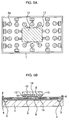
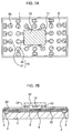
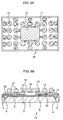
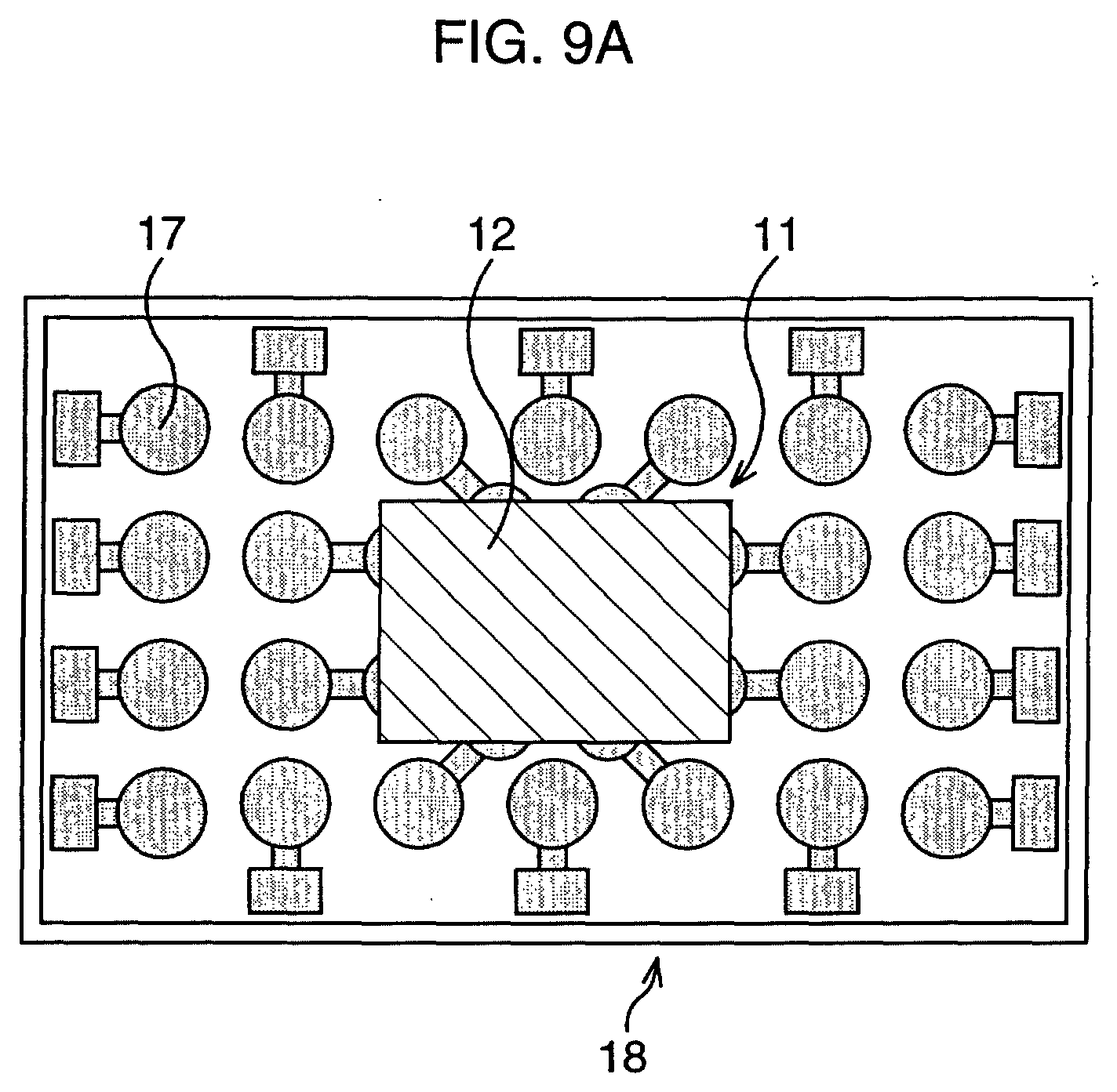
- Figs. 1A to 9B are schematic views illustrating the steps of the method for fabricating the semiconductor package according to the embodiment in the order in which they appear; the A series being a plan view and the B series being a cross-sectional view, respectively.
- an insulating film 2 of polyimide or the like is formed on a semiconductor substrate 1 of silicon.
- the insulating film 2 is ablated through photolithography and the subsequent dry etching to form each groove 4.
- An electrically conductive material is then deposited to fill in the groove 4 and then polished flat such as by chemical mechanical polishing (CMP), thereby forming a plurality of pad electrodes 3 that fill in the groove 4.
- CMP chemical mechanical polishing
- an opening portion 5 is formed through photolithography and the subsequent dry etching.
- an adhesive used for the lamination acts as an insulating material.
- RF radio frequency
- the conductive layer 6 When the sputtering is employed to form the conductive layer 6, it is preferable to form the conductive layer 6 in a multi-layer structure that includes a metal film providing a good adhesion to the insulating film 2 and a metal film having a good electrical property, the films being stacked in layers.
- metals such as Cr or Ti may be used as the metal providing a good adhesion to the insulating film, while metals such as Cu may be used as the metal having a good electrical property.
- the second semiconductor chip is bonded to the element-formed portion 11 of each first semiconductor chip while patterned wires are formed on the element-formed portion 11 of each first semiconductor chip on the conductive layer 6.
- photoresist 7 is first coated on the conductive layer 6. Then, as shown in Figs. 4A and 4B, the photoresist 7 is ablated through photolithography to form a patterned resist 8 having openings 8a that are exposed through the surface of the conductive layer 6 in the shape of the wires.
- a second semiconductor chip 12 is connected to the element-formed portion 11 of each first semiconductor chip.
- the second semiconductor chip 12 has a predetermined semiconductor element fabricated thereon, and is provided with pad electrodes 13 bonded to the first semiconductor chip and adhesive resin 14 used for temporary fixation.
- the pad electrode 13 is provided with bumps 15 in advance about 30 ⁇ m in height.
- the second semiconductor chip 12 is placed oppositely in alignment with the element-formed portion 11 of each first semiconductor chip and the opening portion 5 of the insulating film 2.
- the adhesive resin 14 is bonded to the patterned resist 8 on the element-formed portion 11, thereby fixing temporarily the second semiconductor chip 12 to the element-formed portion 11 of the first semiconductor chip.
- a plated film formed by the electroplating includes a layer such as a copper (Cu) layer provided in consideration of electrical properties, a nickel (Ni) layer acting as a barrier metal, and a gold (Au) layer providing a good adhesion to external connection terminals.
- the Cu layer in the plated film may not be provided so long as the electrical properties can be ensured only with the conductive layer 6.
- the openings of the patterned resist 8 are filled, and a plated film is formed to cover the bumps 15 provided on the pad electrodes 13 of the second semiconductor chip 12.
- the plated film serves as a single-plated (broken) film (film plated in a single process step) that provides a group of wires 16, which includes lead wires 21 and 22 that are formed after (according to) the shape of the opening of the patterned resist 8.
- the lead wire 21 is connected to the pad electrode 3, while the lead wire 22 covers the bumps 15 near the second semiconductor chip 12 to electrically connect the second semiconductor chip 12 to the element-formed portion 11 of the first semiconductor chip.
- the patterned resist 8 is removed by ashing or the like.
- the adhesive resin 14 adhered to the patterned resist 8 remains on the second semiconductor chip 12.
- the conductive layer 6 underlying the patterned resist 8 is removed. Since it is necessary to remove the conductive layer 6 at a portion corresponding to one underlying the second semiconductor chip 12, the conductive layer 6 is removed through wet etching.
- solder balls are provided at terminal-formed portions 21a, 22a of each of the lead wires 21, 22 to form external connection terminals 17.
- the semiconductor substrate 1 is cut, thereby providing a complete semiconductor package in which the group of wires 16 having the external connection terminals 17 is formed on the insulating film 2 and the lead wire 22 bonds the second semiconductor chip 12 to the first semiconductor chip 18.
- electroplating is used to form the aforementioned plated film, however, electroless plating may also be employed.
- the conductive layer 6 or the power supply electrode is not required.
- Employing the electroless plating to form the plated film would cause an unnecessary sidewall to be formed along the edges of the lead wires 21, 22 upon forming the group of wires 16. The sidewall is therefore removed after the second semiconductor chip 12 has been bonded to the element-formed portion 11 of the first semiconductor chip.
- the group of wires 16 that bonds the first semiconductor chip 18 and the second semiconductor chip 12 together and extends on the first semiconductor chip 18 is formed of a single plated film through plating in one continuous process. This makes it possible to bond the second semiconductor chip 12 to the first semiconductor chip 18 at relatively low temperatures without applying a pressure therebetween. Accordingly, this makes it possible to simplify the manufacturing process and reduce the turnaround time, thereby reducing costs. This also makes it possible to prevent damage (break) to the microstructure such as the lead wires 21, 22 and damage to the insulating film 2, thereby providing a semiconductor package that readily ensures the improvement of transmission characteristics.
- this modified example also discloses a semiconductor package having one semiconductor chip bonded onto another, but is slightly different in what manner both the semiconductor chips are bonded together.
- Figs. 10A, 10B, and 10C are schematic cross-sectional views illustrating only main steps of a method for fabricating a semiconductor package according to the modified example of the embodiment.
- connection pad electrodes 31 are formed on the conductive layer 6 that serves as a power supply electrode upon performing electroplating on the semiconductor substrate 1, and a patterned resist 32 is formed so as to provide an opening for exposing at least the pad electrodes 31, as shown in Fig. 10A.
- the second semiconductor chip 12 is connected to the element-formed portion 11 of each first semiconductor chip.
- the second semiconductor chip 12 has a predetermined semiconductor element fabricated thereon, and is provided with the pad electrode 13 bonded to the first semiconductor chip and the adhesive resin 14 used for temporary fixation.
- the pad electrode 13 is provided with a bump 15 in advance so as to cover the pad electrode 13.
- the second semiconductor chip 12 is placed oppositely in alignment with the element-formed portion 11 of each first semiconductor chip.
- the adhesive resin 14 is bonded to the patterned resist 32 on the element-formed portion 11, thereby fixing temporarily the second semiconductor chip 12 to the element-formed portion 11 of the first semiconductor chip.
- a plated film formed by the electroplating includes a layer such as a copper (Cu) layer provided in consideration of electrical properties, a nickel (Ni) layer acting as a barrier metal, and a gold (Au) layer providing a good adhesion to external connection terminals.
- the Cu layer in the plated film may not be provided so long as the electrical properties can be ensured only with the conductive layer 6.
- the opening of the patterned resist 32 is filled, and a single plated film of wires 34 is formed to cover each of upper and lower bumps 13, 33.
- the patterned resist 32 is removed by ashing or the like.
- the adhesive resin 14 adhered to the patterned resist 32 remains on the second semiconductor chip 12.
- the wires 34 that bond the first semiconductor chip 18 and the second semiconductor chip 12 together are formed of a single plated film through plating in one continuous process. This makes it possible to bond the second semiconductor chip 12 to the first semiconductor chip 18 at relatively low temperatures without applying a pressure therebetween. Accordingly, this makes it possible to simplify the manufacturing process and reduce the turnaround time, thereby reducing costs. This also makes it possible to prevent damage (break) to the microstructure and damage to the insulating film 2, thereby providing a semiconductor package that readily ensures the improvement of transmission characteristics.
- a highly reliable semiconductor device is, that provides a simplified manufacturing process and reduced turnaround time, thereby realizing reduced manufacturing costs.
- the semiconductor device can also prevent breaks in the wires and readily ensure the improvement of transmission characteristics.
- embodiments of the present invention provide a group of wires bonding a first semicondutor chip and a second semiconductor chip together which extends on the first semiconductor chip and is formed of a film layer (for example through plating) in one continuous process.
- the second semiconductor chip is then bonded onto the first semiconductor chip to complete a semiconductor package.
Landscapes
- Internal Circuitry In Semiconductor Integrated Circuit Devices (AREA)
- Wire Bonding (AREA)
Abstract
Description
Claims (13)
- A semiconductor device comprising:a first semiconductor chip,a second semiconductor chip bonded onto the first semiconductor chip, anda single electrically conductive film, extending on an element-formed surface of the first semiconductor chip, electrically connecting between the first semiconductor chip and the second semiconductor chip.
- A semiconductor device according to claim 1, wherein the conductive film is a plated film.
- A semiconductor device according to claim 1 or 2, wherein the conductive film also serves as a lead wire of the first semiconductor chip.
- A semiconductor device according to any of the preceding claims, wherein an adhesive resin that has been used for temporarily fixing both the semiconductor chips remains on a surface of the second semiconductor chip opposite to the first semiconductor chip.
- A method for fabricating a semiconductor device having a second semiconductor chip bonded to a first semiconductor chip, comprising the steps of:fixing temporarily an element-formed surface of the first semiconductor chip and an element-formed surface of the second semiconductor chip, the element-formed surfaces being placed opposite to each other, andforming a single electrically conductive film, extending on the element-formed surface of the first semiconductor chip, electrically connecting between the first semiconductor chip and the second semiconductor chip.
- A method for fabricating a semiconductor device according to claim 5, wherein the conductive film is integrated with a lead wire of the first semiconductor chip and a connecting portion to be connected with the second semiconductor chip.
- A method for fabricating a semiconductor device according to claim 5 or 6, wherein the conductive film is formed with the first semiconductor chip and the second semiconductor chip being temporarily fixed and thereby retained relative to each other without applying a pressure therebetween.
- A method for fabricating a semiconductor device according to any of the preceding method claims, wherein the conductive film is formed through plating.
- A method for fabricating a semiconductor device according to claim 8, wherein the step of forming the conductive film includes the steps of:forming a mask having an opening provided in a shape of the lead wire on the first semiconductor chip, andforming the conductive film through plating to fill in the opening of the mask in order to connect the conductive film to the second semiconductor chip.
- A method for fabricating a semiconductor device according to claim 8 or 9, wherein the plating is electroplating or electroless-plating.
- A method for fabricating a semiconductor device according to any of the preceding claims, wherein the temporal fixation is carried out using an adhesive resin.
- A method for fabricating a semiconductor device according to any of the preceding claims, wherein the each second semiconductor chip is bonded to a plurality of the first semiconductor chips being formed on a semiconductor substrate.
- A method for fabricating a semiconductor device according to any of the preceding claims, wherein the film is formed by filling openings in patterned resist, thereby providing separate film layer portions all extending in the same plane.
Applications Claiming Priority (2)
| Application Number | Priority Date | Filing Date | Title |
|---|---|---|---|
| JP2002051929 | 2002-02-27 | ||
| JP2002051929A JP2003258196A (en) | 2002-02-27 | 2002-02-27 | Semiconductor device and manufacturing method thereof |
Publications (2)
| Publication Number | Publication Date |
|---|---|
| EP1341232A2 true EP1341232A2 (en) | 2003-09-03 |
| EP1341232A3 EP1341232A3 (en) | 2005-10-26 |
Family
ID=27678525
Family Applications (1)
| Application Number | Title | Priority Date | Filing Date |
|---|---|---|---|
| EP02255356A Withdrawn EP1341232A3 (en) | 2002-02-27 | 2002-07-31 | Semiconductor device and method for fabricating the same |
Country Status (6)
| Country | Link |
|---|---|
| US (2) | US6734042B2 (en) |
| EP (1) | EP1341232A3 (en) |
| JP (1) | JP2003258196A (en) |
| KR (1) | KR20030071462A (en) |
| CN (1) | CN1441494A (en) |
| TW (1) | TW554443B (en) |
Families Citing this family (5)
| Publication number | Priority date | Publication date | Assignee | Title |
|---|---|---|---|---|
| KR20040060123A (en) * | 2002-12-30 | 2004-07-06 | 동부전자 주식회사 | Method for packaging semiconductor device |
| JP2004363573A (en) * | 2003-05-15 | 2004-12-24 | Kumamoto Technology & Industry Foundation | Semiconductor chip package and method of manufacturing the same |
| US20090014897A1 (en) * | 2003-05-15 | 2009-01-15 | Kumamoto Technology & Industry Foundation | Semiconductor chip package and method of manufacturing the same |
| US7705441B2 (en) * | 2007-03-06 | 2010-04-27 | Infineon Technologies Ag | Semiconductor module |
| JP5472230B2 (en) * | 2011-08-10 | 2014-04-16 | 株式会社村田製作所 | Chip component structure and manufacturing method |
Family Cites Families (9)
| Publication number | Priority date | Publication date | Assignee | Title |
|---|---|---|---|---|
| JPH09326465A (en) * | 1996-06-06 | 1997-12-16 | Matsushita Electric Ind Co Ltd | Semiconductor device and manufacturing method thereof |
| DE69835747T2 (en) * | 1997-06-26 | 2007-09-13 | Hitachi Chemical Co., Ltd. | SUBSTRATE FOR MOUNTING SEMICONDUCTOR CHIPS |
| JP3468132B2 (en) * | 1998-11-20 | 2003-11-17 | 松下電器産業株式会社 | Method for manufacturing semiconductor device |
| JP3365743B2 (en) * | 1999-02-03 | 2003-01-14 | ローム株式会社 | Semiconductor device |
| JP2000228485A (en) * | 1999-02-08 | 2000-08-15 | Rohm Co Ltd | Semiconductor device and semiconductor chip having chip-on-chip structure |
| JP4245754B2 (en) * | 1999-11-02 | 2009-04-02 | パナソニック株式会社 | Semiconductor device |
| JP3631120B2 (en) * | 2000-09-28 | 2005-03-23 | 沖電気工業株式会社 | Semiconductor device |
| JP3565334B2 (en) * | 2001-01-25 | 2004-09-15 | シャープ株式会社 | Semiconductor device, liquid crystal module using the same, and method of manufacturing semiconductor device |
| JP2002314031A (en) * | 2001-04-13 | 2002-10-25 | Fujitsu Ltd | Multi-chip module |
-
2002
- 2002-02-27 JP JP2002051929A patent/JP2003258196A/en active Pending
- 2002-07-30 KR KR1020020044912A patent/KR20030071462A/en not_active Withdrawn
- 2002-07-31 CN CN02127290A patent/CN1441494A/en active Pending
- 2002-07-31 US US10/207,815 patent/US6734042B2/en not_active Expired - Fee Related
- 2002-07-31 EP EP02255356A patent/EP1341232A3/en not_active Withdrawn
- 2002-07-31 TW TW091117220A patent/TW554443B/en not_active IP Right Cessation
-
2004
- 2004-02-17 US US10/778,152 patent/US20050074971A1/en not_active Abandoned
Also Published As
| Publication number | Publication date |
|---|---|
| EP1341232A3 (en) | 2005-10-26 |
| KR20030071462A (en) | 2003-09-03 |
| JP2003258196A (en) | 2003-09-12 |
| US20030162320A1 (en) | 2003-08-28 |
| CN1441494A (en) | 2003-09-10 |
| TW554443B (en) | 2003-09-21 |
| US20050074971A1 (en) | 2005-04-07 |
| US6734042B2 (en) | 2004-05-11 |
Similar Documents
| Publication | Publication Date | Title |
|---|---|---|
| KR100621438B1 (en) | Laminated chip package using photosensitive polymer and manufacturing method thereof | |
| CN100474573C (en) | Semiconductor device and manufacturing method thereof | |
| US7132750B2 (en) | Semiconductor component having conductors with wire bondable metalization layers | |
| JP4431123B2 (en) | Electronic device substrate and manufacturing method thereof, and electronic device and manufacturing method thereof | |
| US20060141669A1 (en) | Semiconductor package having semiconductor constructing body and method of manufacturing the same | |
| JP5942823B2 (en) | Electronic component device manufacturing method, electronic component device, and electronic device | |
| JP2005327984A (en) | Electronic component and method for manufacturing electronic component mounting structure | |
| KR20070096016A (en) | Interconnect structures with bond-pads and methods of forming bump sites on bond-pads | |
| US8012798B2 (en) | Method of fabricating stacked semiconductor chips | |
| JP2001144204A (en) | Semiconductor device and manufacturing method thereof | |
| JP4121542B1 (en) | Manufacturing method of electronic device | |
| CN100524725C (en) | Semiconductor device and manufacturing method of the same | |
| US7704792B2 (en) | Semiconductor device and method of manufacturing the same | |
| US7297575B2 (en) | System semiconductor device and method of manufacturing the same | |
| US7202421B2 (en) | Electronic elements, method for manufacturing electronic elements, circuit substrates, method for manufacturing circuit substrates, electronic devices and method for manufacturing electronic devices | |
| TWI420610B (en) | Semiconductor device and method of manufacturing same | |
| US6734042B2 (en) | Semiconductor device and method for fabricating the same | |
| US20090168380A1 (en) | Package substrate embedded with semiconductor component | |
| CN114171405A (en) | Packaging method and packaging structure of fan-out type stacked chip | |
| JP2000243785A (en) | Manufacturing method of semiconductor chip | |
| US11075180B2 (en) | Semiconductor device and method of manufacturing the semiconductor device | |
| TWI399839B (en) | Intermediary connector built into semiconductor package construction | |
| JP6515243B2 (en) | Semiconductor device manufacturing method | |
| JP2004063808A (en) | Semiconductor device package structure and method of manufacturing the same | |
| JP3819306B2 (en) | Bonded body of semiconductor element and supporting substrate, and method for manufacturing the semiconductor device |
Legal Events
| Date | Code | Title | Description |
|---|---|---|---|
| PUAI | Public reference made under article 153(3) epc to a published international application that has entered the european phase |
Free format text: ORIGINAL CODE: 0009012 |
|
| AK | Designated contracting states |
Kind code of ref document: A2 Designated state(s): AT BE BG CH CY CZ DE DK EE ES FI FR GB GR IE IT LI LU MC NL PT SE SK TR |
|
| AX | Request for extension of the european patent |
Extension state: AL LT LV MK RO SI |
|
| PUAL | Search report despatched |
Free format text: ORIGINAL CODE: 0009013 |
|
| AK | Designated contracting states |
Kind code of ref document: A3 Designated state(s): AT BE BG CH CY CZ DE DK EE ES FI FR GB GR IE IT LI LU MC NL PT SE SK TR |
|
| AX | Request for extension of the european patent |
Extension state: AL LT LV MK RO SI |
|
| AKX | Designation fees paid | ||
| REG | Reference to a national code |
Ref country code: DE Ref legal event code: 8566 |
|
| STAA | Information on the status of an ep patent application or granted ep patent |
Free format text: STATUS: THE APPLICATION IS DEEMED TO BE WITHDRAWN |
|
| 18D | Application deemed to be withdrawn |
Effective date: 20060427 |