EP1341227A2 - Interconnection structure in semiconductor devices and method for making the same - Google Patents
Interconnection structure in semiconductor devices and method for making the same Download PDFInfo
- Publication number
- EP1341227A2 EP1341227A2 EP03100227A EP03100227A EP1341227A2 EP 1341227 A2 EP1341227 A2 EP 1341227A2 EP 03100227 A EP03100227 A EP 03100227A EP 03100227 A EP03100227 A EP 03100227A EP 1341227 A2 EP1341227 A2 EP 1341227A2
- Authority
- EP
- European Patent Office
- Prior art keywords
- layer
- dopant
- conductive layer
- dielectric
- semiconductor device
- Prior art date
- Legal status (The legal status is an assumption and is not a legal conclusion. Google has not performed a legal analysis and makes no representation as to the accuracy of the status listed.)
- Ceased
Links
Images


Classifications
-
- H—ELECTRICITY
- H10—SEMICONDUCTOR DEVICES; ELECTRIC SOLID-STATE DEVICES NOT OTHERWISE PROVIDED FOR
- H10W—GENERIC PACKAGES, INTERCONNECTIONS, CONNECTORS OR OTHER CONSTRUCTIONAL DETAILS OF DEVICES COVERED BY CLASS H10
- H10W20/00—Interconnections in chips, wafers or substrates
- H10W20/01—Manufacture or treatment
- H10W20/031—Manufacture or treatment of conductive parts of the interconnections
- H10W20/032—Manufacture or treatment of conductive parts of the interconnections of conductive barrier, adhesion or liner layers
- H10W20/033—Manufacture or treatment of conductive parts of the interconnections of conductive barrier, adhesion or liner layers in openings in dielectrics
- H10W20/034—Manufacture or treatment of conductive parts of the interconnections of conductive barrier, adhesion or liner layers in openings in dielectrics bottomless barrier, adhesion or liner layers
-
- H—ELECTRICITY
- H10—SEMICONDUCTOR DEVICES; ELECTRIC SOLID-STATE DEVICES NOT OTHERWISE PROVIDED FOR
- H10W—GENERIC PACKAGES, INTERCONNECTIONS, CONNECTORS OR OTHER CONSTRUCTIONAL DETAILS OF DEVICES COVERED BY CLASS H10
- H10W20/00—Interconnections in chips, wafers or substrates
- H10W20/01—Manufacture or treatment
- H10W20/031—Manufacture or treatment of conductive parts of the interconnections
- H10W20/032—Manufacture or treatment of conductive parts of the interconnections of conductive barrier, adhesion or liner layers
- H10W20/033—Manufacture or treatment of conductive parts of the interconnections of conductive barrier, adhesion or liner layers in openings in dielectrics
- H10W20/037—Manufacture or treatment of conductive parts of the interconnections of conductive barrier, adhesion or liner layers in openings in dielectrics the barrier, adhesion or liner layers being on top of a main fill metal
-
- H—ELECTRICITY
- H10—SEMICONDUCTOR DEVICES; ELECTRIC SOLID-STATE DEVICES NOT OTHERWISE PROVIDED FOR
- H10W—GENERIC PACKAGES, INTERCONNECTIONS, CONNECTORS OR OTHER CONSTRUCTIONAL DETAILS OF DEVICES COVERED BY CLASS H10
- H10W20/00—Interconnections in chips, wafers or substrates
- H10W20/01—Manufacture or treatment
- H10W20/031—Manufacture or treatment of conductive parts of the interconnections
- H10W20/032—Manufacture or treatment of conductive parts of the interconnections of conductive barrier, adhesion or liner layers
- H10W20/042—Manufacture or treatment of conductive parts of the interconnections of conductive barrier, adhesion or liner layers the barrier, adhesion or liner layers being seed or nucleation layers
- H10W20/043—Manufacture or treatment of conductive parts of the interconnections of conductive barrier, adhesion or liner layers the barrier, adhesion or liner layers being seed or nucleation layers for electroplating
-
- H—ELECTRICITY
- H10—SEMICONDUCTOR DEVICES; ELECTRIC SOLID-STATE DEVICES NOT OTHERWISE PROVIDED FOR
- H10W—GENERIC PACKAGES, INTERCONNECTIONS, CONNECTORS OR OTHER CONSTRUCTIONAL DETAILS OF DEVICES COVERED BY CLASS H10
- H10W20/00—Interconnections in chips, wafers or substrates
- H10W20/01—Manufacture or treatment
- H10W20/031—Manufacture or treatment of conductive parts of the interconnections
- H10W20/032—Manufacture or treatment of conductive parts of the interconnections of conductive barrier, adhesion or liner layers
- H10W20/042—Manufacture or treatment of conductive parts of the interconnections of conductive barrier, adhesion or liner layers the barrier, adhesion or liner layers being seed or nucleation layers
- H10W20/044—Manufacture or treatment of conductive parts of the interconnections of conductive barrier, adhesion or liner layers the barrier, adhesion or liner layers being seed or nucleation layers for electroless plating
-
- H—ELECTRICITY
- H10—SEMICONDUCTOR DEVICES; ELECTRIC SOLID-STATE DEVICES NOT OTHERWISE PROVIDED FOR
- H10W—GENERIC PACKAGES, INTERCONNECTIONS, CONNECTORS OR OTHER CONSTRUCTIONAL DETAILS OF DEVICES COVERED BY CLASS H10
- H10W20/00—Interconnections in chips, wafers or substrates
- H10W20/01—Manufacture or treatment
- H10W20/031—Manufacture or treatment of conductive parts of the interconnections
- H10W20/032—Manufacture or treatment of conductive parts of the interconnections of conductive barrier, adhesion or liner layers
- H10W20/052—Manufacture or treatment of conductive parts of the interconnections of conductive barrier, adhesion or liner layers by treatments not introducing additional elements therein
- H10W20/0526—Manufacture or treatment of conductive parts of the interconnections of conductive barrier, adhesion or liner layers by treatments not introducing additional elements therein by thermal treatment thereof
-
- H—ELECTRICITY
- H10—SEMICONDUCTOR DEVICES; ELECTRIC SOLID-STATE DEVICES NOT OTHERWISE PROVIDED FOR
- H10W—GENERIC PACKAGES, INTERCONNECTIONS, CONNECTORS OR OTHER CONSTRUCTIONAL DETAILS OF DEVICES COVERED BY CLASS H10
- H10W20/00—Interconnections in chips, wafers or substrates
- H10W20/01—Manufacture or treatment
- H10W20/031—Manufacture or treatment of conductive parts of the interconnections
- H10W20/032—Manufacture or treatment of conductive parts of the interconnections of conductive barrier, adhesion or liner layers
- H10W20/055—Manufacture or treatment of conductive parts of the interconnections of conductive barrier, adhesion or liner layers by formation methods other than physical vapour deposition [PVD], chemical vapour deposition [CVD] or liquid deposition
-
- H—ELECTRICITY
- H10—SEMICONDUCTOR DEVICES; ELECTRIC SOLID-STATE DEVICES NOT OTHERWISE PROVIDED FOR
- H10W—GENERIC PACKAGES, INTERCONNECTIONS, CONNECTORS OR OTHER CONSTRUCTIONAL DETAILS OF DEVICES COVERED BY CLASS H10
- H10W20/00—Interconnections in chips, wafers or substrates
- H10W20/01—Manufacture or treatment
- H10W20/031—Manufacture or treatment of conductive parts of the interconnections
- H10W20/056—Manufacture or treatment of conductive parts of the interconnections by filling conductive material into holes, grooves or trenches
-
- H—ELECTRICITY
- H10—SEMICONDUCTOR DEVICES; ELECTRIC SOLID-STATE DEVICES NOT OTHERWISE PROVIDED FOR
- H10W—GENERIC PACKAGES, INTERCONNECTIONS, CONNECTORS OR OTHER CONSTRUCTIONAL DETAILS OF DEVICES COVERED BY CLASS H10
- H10W20/00—Interconnections in chips, wafers or substrates
- H10W20/01—Manufacture or treatment
- H10W20/031—Manufacture or treatment of conductive parts of the interconnections
- H10W20/064—Manufacture or treatment of conductive parts of the interconnections by modifying the conductivity of conductive parts, e.g. by alloying
- H10W20/065—Manufacture or treatment of conductive parts of the interconnections by modifying the conductivity of conductive parts, e.g. by alloying by making at least a portion of the conductive part non-conductive, e.g. by oxidation
Definitions
- the present invention relates generally to the field of semiconductor devices. Specifically, the invention relates to semiconductor devices using copper interconnect lines, and methods of manufacturing such semiconductor devices.
- a known method of manufacturing a known semiconductor device having copper interconnect lines includes the steps of forming a dielectric layer 104 over a semiconductor substrate 102, and etching a plurality of trenches or a plurality of vias 106, or both, into dielectric layer 104. Because copper atoms diffuse readily into other materials, e.g., dielectric materials, such known methods also include the step of forming a barrier layer 110, i.e., a metal barrier layer or a dielectric barrier layer, within trenches or vias 106.
- a barrier layer 110 i.e., a metal barrier layer or a dielectric barrier layer
- known dielectric barrier layers may comprise SiN, SiC, SiCN, or similar dielectric compounds which, when used in a layer of sufficient thickness, substantially reduces or prevents the diffusion of copper atoms from one material to another material.
- known metal barrier layers may comprise Ta, TaN, TiN, or similar metal compounds which, when used in a layer of sufficient thickness, substantially reduces or prevents the diffusion of copper atoms from one material to another material. This method also includes the steps of forming a pure copper seed layer 112 over barrier layer 110 and forming a pure copper plate layer 120 over pure copper seed layer 112.
- etch stop layer may comprise SiN, SiC, SiCN, or similar dielectric compounds which, when used in a layer of sufficient thickness, substantially reduces or prevents the diffusion of copper atoms from one material to another material.
- the impurities may be added to the known metal barriers in order to decrease the permeability of the metal compound.
- the impurities may allow the known metal barriers to substantially reduce or prevent the diffusion of copper atoms from one material to another material, the impurities increase the resistivity of the metal barrier layer.
- the resistivity of the metal barrier layer may be ten times greater than the resistivity of the copper layers, which difference degrades the performance of the semiconductor device.
- the dielectric compounds used in known dielectric barrier layers may have an associated dielectric constant between 4.5 and 8.0, which degrades the performance of the semiconductor device.
- the dielectric barrier layer is of a thickness suitable for substantially reducing or preventing copper atoms from diffusing from one material to another material, which further degrades the performance of the semiconductor device.
- At least one conductive layer e.g., the seed layer or the plate layer, or both, may comprise at least one dopant, e.g., magnesium, indium, tin, or the like.
- the at least one conductive layer is annealed at a predetermined temperature, and the at least one dopant diffuses to the surface of at least one side of the at least one conductive layer and is exposed to oxygen, at least one dopant oxide layer is formed at that side of the conductive layer.
- the at least one dopant may diffuse to the surface of the top side of the at least one conductive layer, such that the at least one dopant is exposed to oxygen.
- a dopant oxide layer having a reduced thickness and improved adhesive qualities relative to known metal or dielectric barrier layers may be formed at the surface of the top side of the at least one conductive layer.
- the at least one dopant oxide layer substantially reduces or prevents the diffusion of atoms e.g., copper atoms, from one material to another material.
- another technical advantage of the present invention is that the semiconductor device may be manufactured without a metal or dielectric barrier layer.
- the etch stop layer when an etch stop layer is formed over the at least one dopant oxide layer, because the dopant oxide layer substantially reduces or prevents the diffusion of from one material to another material, the etch stop layer does not have to substantially reduce or prevent the diffusion of atoms.
- a method of manufacturing a semiconductor device comprises the steps of providing a semiconductor substrate, forming a dielectric layer over the semiconductor substrate, and etching at least one trench or at least one via in the dielectric layer.
- the method also comprises the steps of forming at least one conductive layer comprising at least one dopant in the trench or the via.
- the method further comprises the steps of polishing the at least one conductive layer and annealing the at least one conductive layer at a predetermined temperature.
- the at least one dopant diffuses substantially to the surface of at least one side of the at least one conductive layer when the at least one conductive layer is annealed at the predetermined temperature, and forms a dopant oxide layer when exposed to oxygen.
- a method of manufacturing a semiconductor device comprises the steps of providing a semiconductor substrate, forming a dielectric layer over the semiconductor substrate, and etching at least one trench or at least one via in the dielectric layer.
- the method also comprises the steps of forming a seed layer comprising copper in the trench or the via, and forming a plate layer comprising copper over at least a portion of the seed layer.
- the method further comprises the steps of polishing the plate layer and thermally annealing the seed layer or the plate layer, or both at a predetermined temperature.
- the seed layer or the plate layer, or both further comprises a dopant
- the at least one dopant diffuses substantially to the surface of at least one side of the plate layer when the seed layer or the plate layer, or both, is annealed at the predetermined temperature, and forms a dopant oxide layer when exposed to oxygen.
- a semiconductor device comprising a semiconductor substrate and a dielectric layer formed over the semiconductor substrate.
- the semiconductor device also comprises at least one conductive layer formed in a trench or a via within the dielectric layer.
- the at least one conductive layer comprises at least one copper layer, and also may comprise at least one dopant oxide layer formed substantially at the surface of at least one side of the at least one conductive layer, e.g., the surface of the top side of the at least one conductive layer.
- a method of manufacturing a semiconductor device are described.
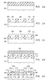
- a semiconductor substrate 202 is provided, and in step 304, a dielectric layer 204 may be formed over semiconductor substrate 202.
- Dielectric layer 204 may comprise any known dielectric material having a low dielectric constant, e.g., about 4.5 or less.
- dielectric layer 204 may comprise silicon dioxide (SiO 2 ), plasma-enhanced tetraethyl orthosilicate, borophosphosilicate glass, organic silicate glass, or the like.
- dielectric layer 204 may be formed on, and may be in direct contact with, semiconductor substrate 202 along the entire surface of semiconductor substrate 202.
- at least one trench or at least one via 206 e.g., a plurality of trenches or a plurality of vias, or both, may be etched in dielectric layer 204, such that dielectric layer 204 no longer may be formed over the entire surface of semiconductor substrate 202 and a portion of the surface of semiconductor substrate 202 is exposed.
- trenches or vias 206 may be etched in areas where interconnect lines or structures, e.g., copper interconnect lines or structures, may be disposed.
- At least one conductive layer e.g., a seed layer 212 or a plate layer 220, or both, may be formed within trenches or vias 206.
- the at least one conductive layer may comprise copper and at least one dopant, e.g., tin, magnesium, indium, or the like.
- the at least one dopant may be added to the at least one conductive layer by any known incorporation method.
- the at least one dopant may be added using physical vapor deposition, chemical vapor deposition, atomic layer deposition, co-plating, or the like.
- step 308 may comprise steps 308a and 308b.
- a seed layer 212 comprising copper may be formed over dielectric layer 204, such that at least a portion of seed layer 212 may be disposed within trenches or vias 206 and may be formed over a portion of semiconductor substrate 202.
- a plate layer 220 comprising copper may be formed over seed layer 212, such that at least a portion of plate layer 220 also may be disposed within trenches or vias 206.
- seed layer 212 or plate layer 220, or both further may comprise the at least one dopant.
- plate layer 220 may be polished, e.g., by any known chemical-mechanical polishing process.
- those portions of plate layer 220 formed outside trenches or vias 206 may be removed.
- those portions of seed layer 212 formed outside trenches or vias 206 also may be removed, such that at least a portion of seed layer 212, at least a portion of plate layer 220, and at least a portion of dielectric layer 204 are exposed.
- the at least one conductive layer may be thermally annealed, i.e., heated and subsequently cooled in order to toughen and reduce brittleness, at a predetermined temperature.
- the predetermined temperature may be between about 100° C and about 400° C.
- the predetermined temperature may be any temperature sufficient to diffuse a selected dopant to the surface of at least one side of the at least one conductive layer without damaging other components of the semiconductor device.
- the amount of time sufficient to diffuse may depend on the temperature at which the at least one conductive layer is annealed and the chemical properties of the particular dopant.
- the at least conductive layer is thermally annealed subsequent to the step of polishing.
- the at least one dopant within the at least one conductive layer may diffuse substantially to the surface of at least one side of the at least one conductive layer, and may form at least one dopant oxide layer when exposed to oxygen.
- the at least one conductive layer comprises plate layer 220, and the at least one dopant diffuses to the surface of plate layer 220, the at least one dopant is exposed to oxygen and the at least one dopant is oxidized.
- a dopant oxide layer 220a is formed at a first or a top side of plate layer 220, such that plate layer 220 is divided into dopant oxide layer 220a and a copper layer 220b.
- the at least one conductive layer comprises seed layer 212 and the at least one dopant diffuses to the surface of seed layer 212 and is oxidized
- a dopant oxide layer 212a may be formed at a first or a top side of seed layer 212.
- a dopant oxide layer 212c may be formed at a second side of seed layer 212
- a dopant oxide layer 212d may be formed at a third side of seed layer 212.
- dopant oxide layers 212c and 212d may be formed when the at least one dopant diffuses to the surface of the second and third sides of seed layer 212, respectively, and is exposed to oxygen contained within dielectric layer 204.
- seed layer 212 may be divided into dopant oxide layer 212a, 212c, or 212d, or a combination thereof, and a copper layer 212b.
- dopant oxide layers 212a, 212c, 212d, or 220a, or a combination thereof may substantially reduce or prevent copper atoms from diffusing from one material to another material.
- a dopant oxide layer (not shown) also may be formed at a fourth or bottom side of seed layer 212, such that a dopant oxide layer contacts at least a portion of substrate 202.
- the method also may comprise the step of forming a first etch stop layer (not shown) over at least a portion of plate layer 220, such that additional levels of copper interconnect lines may be manufactured.
- the first etch stop layer may comprise SiO 2 ,. SiN, SiC, or the like.
- the first etch stop may comprise a dielectric compound having increased stop etch qualities, irrespective of the diffusion prevention qualities of the dielectric compound, without substantially degrading the performance of the semiconductor device.
- the semiconductor device may comprise a semiconductor substrate 202 and a dielectric layer 204 formed over at least a portion of semiconductor substrate 202.
- Dielectric layer 204 may comprise any known dielectric material having a low dielectric constant, e.g., about 4.5 or less.
- dielectric layer 204 may comprise silicon dioxide (SiO 2 ) , plasma-enhanced tetraethyl orthosilicate, borophosphosilicate glass, or the like.
- the semiconductor device also may comprise at least one conductive layer formed in a trench or a via 206 within dielectric layer 204.
- the at least one conductive layer may comprise at least one copper layer, and also may comprise at least one dopant oxide layer, e.g., tin oxide, magnesium oxide, indium oxide, or the like.
- the at least one conductive layer may comprise a seed layer 212.
- Seed layer 212 may comprise a copper layer 212b and may be formed over dielectric layer 204.
- the at least one conductive layer also may comprise a plate layer 220. Plate layer 220 may comprise a copper layer 220b and may be formed over seed layer 212.
- seed layer 212 or plate layer 220, or both further may comprise at least one dopant oxide layer, e.g., dopant oxide layers 212a, 212c, or 212d, or a combination thereof, and dopant oxide layer 220a, respectively.
- dopant oxide layer e.g., dopant oxide layers 212a, 212c, or 212d, or a combination thereof, and dopant oxide layer 220a, respectively.
- a dopant oxide layer 220a may be formed at a first or a top side of plate layer 220.
- plate layer 220 may be divided into dopant oxide layer 220a and copper layer 220b.
- a dopant oxide layer 212a may be formed at a first or a top side of seed layer 212.
- a dopant oxide layer 212c may be formed at a second side of seed layer 212, and a dopant oxide layer 212d may be formed at a third side of seed layer 212.
- seed layer 212 may be divided into dopant oxide layer 212a, 212c, or 212d, or a combination thereof, and copper layer 212b.
- dopant oxide layers 212a, 212c, 212d, or 220a, or a combination thereof may substantially reduce or prevent atoms, e.g., copper atoms, from diffusing from one material to another material.
- the semiconductor device also may comprise a first etch stop layer (not shown) formed over at least a portion of plate layer 220, such that additional levels of copper interconnect lines may be manufactured.
- the first stop etch layer may comprise SiO 2 , SiN, SiC, or the like.
Landscapes
- Internal Circuitry In Semiconductor Integrated Circuit Devices (AREA)
- Formation Of Insulating Films (AREA)
Abstract
Description
Claims (10)
- A method of manufacturing a semiconductor device comprising the steps of:providing a semiconductor substrate;forming a dielectric layer over said semiconductor substrate;etching at least one trench or at least one via in said dielectric layer to expose a portion of a surface of said semiconductor substrate;forming at least one conductive layer within said trench or said via, wherein said at least one conductive layer comprises at least one dopant;polishing at least a portion of said at least one conductive layer; andthermally annealing said at least one conductive layer at a predetermined temperature.
- The method of claim 1, wherein said at least one conductive layer further comprises copper.
- The method of claim 2, wherein said at least one dopant diffuses substantially to the surface of at least one side of said at least one conductive layer to form at least one dopant oxide layer and at least one copper layer when said at least one conductive layer is thermally annealed at said predetermined temperature and said at least one dopant is exposed to oxygen.
- The method of claim 3, wherein said at least one dopant comprises magnesium.
- The method of claim 3, wherein said at least one dopant comprises indium.
- The method of claim 3, wherein said at least one dopant comprises tin.
- A semiconductor device comprising:a semiconductor substrate;a dielectric layer formed over at least a portion of said semiconductor substrate;at least one conductive layer formed in a trench or a via within said dielectric layer, wherein said at least one conductive layer comprises:at least one copper layer; andat least one dopant oxide layer formed substantially at the surface of at least one side of said at least one conductive layer.
- The semiconductor device of claim 7, wherein said at least one dopant oxide layer comprises magnesium oxide.
- The semiconductor device of claim 7 or 8, wherein said at least one dopant oxide layer comprises indium oxide.
- The semiconductor device of any one of claims 7 to 9, wherein said at least one dopant oxide layer comprises tin oxide.
Applications Claiming Priority (2)
| Application Number | Priority Date | Filing Date | Title |
|---|---|---|---|
| US35869802P | 2002-02-25 | 2002-02-25 | |
| US358698 | 2002-02-25 |
Publications (2)
| Publication Number | Publication Date |
|---|---|
| EP1341227A2 true EP1341227A2 (en) | 2003-09-03 |
| EP1341227A3 EP1341227A3 (en) | 2004-12-15 |
Family
ID=27734765
Family Applications (1)
| Application Number | Title | Priority Date | Filing Date |
|---|---|---|---|
| EP03100227A Ceased EP1341227A3 (en) | 2002-02-25 | 2003-02-04 | Interconnection structure in semiconductor devices and method for making the same |
Country Status (3)
| Country | Link |
|---|---|
| US (2) | US6911394B2 (en) |
| EP (1) | EP1341227A3 (en) |
| JP (1) | JP2004006669A (en) |
Families Citing this family (17)
| Publication number | Priority date | Publication date | Assignee | Title |
|---|---|---|---|---|
| EP1517972A4 (en) * | 2002-06-07 | 2009-12-16 | Showa Denko Kk | METAL POLISHING COMPOSITION, POLISHING METHOD USING THE SAME, AND METHOD OF PRODUCING SEMICONDUCTOR WAFER USING THE POLISHING METHOD |
| US7482533B2 (en) | 2005-02-22 | 2009-01-27 | Medusa Special Projects, Llc | Nuclear-cored battery |
| US20060185975A1 (en) * | 2005-02-22 | 2006-08-24 | Pentam, Inc. | Decomposition unit |
| US20060185722A1 (en) * | 2005-02-22 | 2006-08-24 | Pentam, Inc. | Method of pre-selecting the life of a nuclear-cored product |
| US7438789B2 (en) * | 2005-02-22 | 2008-10-21 | Medusa Special Projects, Llc | Decomposition cell |
| US20060185153A1 (en) * | 2005-02-22 | 2006-08-24 | Pentam, Inc. | Method of making crystalline to surround a nuclear-core of a nuclear-cored battery |
| US20060185720A1 (en) * | 2005-02-22 | 2006-08-24 | Pentam, Inc. | Method of recycling a nuclear-cored battery |
| JP4589835B2 (en) * | 2005-07-13 | 2010-12-01 | 富士通セミコンダクター株式会社 | Semiconductor device manufacturing method and semiconductor device |
| JP2007059734A (en) * | 2005-08-26 | 2007-03-08 | Sony Corp | Semiconductor device manufacturing method and semiconductor device |
| US7423347B2 (en) * | 2006-01-19 | 2008-09-09 | Taiwan Semiconductor Manufacturing Company, Ltd. | In-situ deposition for cu hillock suppression |
| JP2008135569A (en) * | 2006-11-28 | 2008-06-12 | Rohm Co Ltd | Method of manufacturing semiconductor device, and semiconductor device |
| US8247322B2 (en) * | 2007-03-01 | 2012-08-21 | Taiwan Semiconductor Manufacturing Co., Ltd. | Via/contact and damascene structures and manufacturing methods thereof |
| US7745848B1 (en) * | 2007-08-15 | 2010-06-29 | Nitronex Corporation | Gallium nitride material devices and thermal designs thereof |
| KR101132303B1 (en) * | 2009-02-16 | 2012-04-05 | 주식회사 하이닉스반도체 | Method for forming copper wiring of semiconductor device |
| US9295163B2 (en) | 2013-05-30 | 2016-03-22 | Dyi-chung Hu | Method of making a circuit board structure with embedded fine-pitch wires |
| JP5694503B2 (en) * | 2013-12-27 | 2015-04-01 | Jx日鉱日石金属株式会社 | SEED LAYER WITH SELF-DIFFUSION SUPPRESSING FUNCTION AND METHOD FOR FORMING SEED LAYER HAVING SELF-DIFFUSION SUPPRESSING FUNCTION |
| CN105633012A (en) * | 2015-03-31 | 2016-06-01 | 中国科学院微电子研究所 | Interconnect structure and manufacturing method thereof |
Family Cites Families (18)
| Publication number | Priority date | Publication date | Assignee | Title |
|---|---|---|---|---|
| US4521441A (en) * | 1983-12-19 | 1985-06-04 | Motorola, Inc. | Plasma enhanced diffusion process |
| US4965655A (en) * | 1987-12-10 | 1990-10-23 | Minnesota Mining And Manufacturing Company | Interconnected semiconductor devices |
| US5747360A (en) * | 1993-09-17 | 1998-05-05 | Applied Materials, Inc. | Method of metalizing a semiconductor wafer |
| JP3297220B2 (en) * | 1993-10-29 | 2002-07-02 | 株式会社東芝 | Semiconductor device manufacturing method and semiconductor device |
| US5766379A (en) | 1995-06-07 | 1998-06-16 | The Research Foundation Of State University Of New York | Passivated copper conductive layers for microelectronic applications and methods of manufacturing same |
| US6268291B1 (en) | 1995-12-29 | 2001-07-31 | International Business Machines Corporation | Method for forming electromigration-resistant structures by doping |
| US5913147A (en) | 1997-01-21 | 1999-06-15 | Advanced Micro Devices, Inc. | Method for fabricating copper-aluminum metallization |
| US6387805B2 (en) * | 1997-05-08 | 2002-05-14 | Applied Materials, Inc. | Copper alloy seed layer for copper metallization |
| US6249055B1 (en) | 1998-02-03 | 2001-06-19 | Advanced Micro Devices, Inc. | Self-encapsulated copper metallization |
| JP3568385B2 (en) * | 1998-03-16 | 2004-09-22 | 沖電気工業株式会社 | Method for manufacturing semiconductor device |
| US6022808A (en) * | 1998-03-16 | 2000-02-08 | Advanced Micro Devices, Inc. | Copper interconnect methodology for enhanced electromigration resistance |
| US6147000A (en) * | 1998-08-11 | 2000-11-14 | Advanced Micro Devices, Inc. | Method for forming low dielectric passivation of copper interconnects |
| US6294836B1 (en) * | 1998-12-22 | 2001-09-25 | Cvc Products Inc. | Semiconductor chip interconnect barrier material and fabrication method |
| US6309959B1 (en) | 2000-08-03 | 2001-10-30 | Advanced Micro Devices, Inc. | Formation of self-aligned passivation for interconnect to minimize electromigration |
| US6800554B2 (en) * | 2000-12-18 | 2004-10-05 | Intel Corporation | Copper alloys for interconnections having improved electromigration characteristics and methods of making same |
| US6674170B1 (en) * | 2000-12-18 | 2004-01-06 | Advanced Micro Devices, Inc. | Barrier metal oxide interconnect cap in integrated circuits |
| US6834068B2 (en) * | 2001-06-29 | 2004-12-21 | Matsushita Electric Industrial Co., Ltd. | Semiconductor laser device and method for fabricating the same |
| US6717266B1 (en) * | 2002-06-18 | 2004-04-06 | Advanced Micro Devices, Inc. | Use of an alloying element to form a stable oxide layer on the surface of metal features |
-
2003
- 2003-01-13 US US10/340,932 patent/US6911394B2/en not_active Expired - Lifetime
- 2003-02-04 EP EP03100227A patent/EP1341227A3/en not_active Ceased
- 2003-02-24 JP JP2003045814A patent/JP2004006669A/en not_active Abandoned
-
2004
- 2004-10-14 US US10/964,963 patent/US7187080B2/en not_active Expired - Lifetime
Also Published As
| Publication number | Publication date |
|---|---|
| EP1341227A3 (en) | 2004-12-15 |
| US6911394B2 (en) | 2005-06-28 |
| US20030160332A1 (en) | 2003-08-28 |
| JP2004006669A (en) | 2004-01-08 |
| US20050048784A1 (en) | 2005-03-03 |
| US7187080B2 (en) | 2007-03-06 |
Similar Documents
| Publication | Publication Date | Title |
|---|---|---|
| US6310300B1 (en) | Fluorine-free barrier layer between conductor and insulator for degradation prevention | |
| US6911394B2 (en) | Semiconductor devices and methods of manufacturing such semiconductor devices | |
| US6051508A (en) | Manufacturing method of semiconductor device | |
| TWI484554B (en) | Semiconductor device and manufacturing method thereof | |
| CN101271892B (en) | Semiconductor device and manufacturing method of the same | |
| US9412651B2 (en) | Air-gap formation in interconnect structures | |
| US6603166B2 (en) | Frontside contact on silicon-on-insulator substrate | |
| US20070252277A1 (en) | Semiconductor devices and fabrication method thereof | |
| JP2002289689A (en) | Semiconductor integrated circuit device and method of manufacturing the same | |
| KR20010004598A (en) | method of forming gate for semiconductor device | |
| US7179734B2 (en) | Method for forming dual damascene pattern | |
| US20080048332A1 (en) | Method for forming intermetal dielectric in semiconductor device | |
| US20120146225A1 (en) | Damascene structure | |
| US6833291B2 (en) | Semiconductor processing methods | |
| US7687392B2 (en) | Semiconductor device having metal wiring and method for fabricating the same | |
| US20080157375A1 (en) | Semiconductor device having a metal interconnection and method of fabricating the same | |
| US6133628A (en) | Metal layer interconnects with improved performance characteristics | |
| US8836122B2 (en) | Semiconductor device having copper wiring with increased migration resistance | |
| EP1237182A2 (en) | Aggregate dielectric layer to reduce nitride consumption | |
| US6544886B2 (en) | Process for isolating an exposed conducting surface | |
| JPH04296041A (en) | Semiconductor device and manufacture thereof | |
| KR100855285B1 (en) | Manufacturing method of semiconductor device | |
| KR100571386B1 (en) | Copper wiring of semiconductor device and manufacturing method thereof | |
| KR100784105B1 (en) | Manufacturing Method of Semiconductor Device | |
| KR20090015643A (en) | Metal wiring formation method of semiconductor device |
Legal Events
| Date | Code | Title | Description |
|---|---|---|---|
| PUAI | Public reference made under article 153(3) epc to a published international application that has entered the european phase |
Free format text: ORIGINAL CODE: 0009012 |
|
| AK | Designated contracting states |
Kind code of ref document: A2 Designated state(s): AT BE BG CH CY CZ DE DK EE ES FI FR GB GR HU IE IT LI LU MC NL PT SE SI SK TR |
|
| AX | Request for extension of the european patent |
Extension state: AL LT LV MK RO |
|
| PUAL | Search report despatched |
Free format text: ORIGINAL CODE: 0009013 |
|
| AK | Designated contracting states |
Kind code of ref document: A3 Designated state(s): AT BE BG CH CY CZ DE DK EE ES FI FR GB GR HU IE IT LI LU MC NL PT SE SI SK TR |
|
| AX | Request for extension of the european patent |
Extension state: AL LT LV MK RO |
|
| 17P | Request for examination filed |
Effective date: 20050615 |
|
| AKX | Designation fees paid |
Designated state(s): DE FR GB |
|
| 17Q | First examination report despatched |
Effective date: 20070309 |
|
| STAA | Information on the status of an ep patent application or granted ep patent |
Free format text: STATUS: THE APPLICATION HAS BEEN REFUSED |
|
| 18R | Application refused |
Effective date: 20080713 |