EP1339137A2 - Arc discharge suppressive terminal pair - Google Patents
Arc discharge suppressive terminal pair Download PDFInfo
- Publication number
- EP1339137A2 EP1339137A2 EP03004228A EP03004228A EP1339137A2 EP 1339137 A2 EP1339137 A2 EP 1339137A2 EP 03004228 A EP03004228 A EP 03004228A EP 03004228 A EP03004228 A EP 03004228A EP 1339137 A2 EP1339137 A2 EP 1339137A2
- Authority
- EP
- European Patent Office
- Prior art keywords
- arc discharge
- layer
- terminal
- discharge suppressive
- terminal pair
- Prior art date
- Legal status (The legal status is an assumption and is not a legal conclusion. Google has not performed a legal analysis and makes no representation as to the accuracy of the status listed.)
- Granted
Links
- 238000010891 electric arc Methods 0.000 title claims abstract description 168
- 229910052751 metal Inorganic materials 0.000 claims abstract description 66
- 239000002184 metal Substances 0.000 claims abstract description 66
- 238000002844 melting Methods 0.000 claims abstract description 46
- 230000008018 melting Effects 0.000 claims abstract description 16
- 239000000463 material Substances 0.000 claims abstract description 11
- 238000007747 plating Methods 0.000 claims description 76
- WFKWXMTUELFFGS-UHFFFAOYSA-N tungsten Chemical compound [W] WFKWXMTUELFFGS-UHFFFAOYSA-N 0.000 claims description 27
- 229910052721 tungsten Inorganic materials 0.000 claims description 27
- 239000010937 tungsten Substances 0.000 claims description 27
- BASFCYQUMIYNBI-UHFFFAOYSA-N platinum Chemical compound [Pt] BASFCYQUMIYNBI-UHFFFAOYSA-N 0.000 claims description 22
- ZOKXTWBITQBERF-UHFFFAOYSA-N Molybdenum Chemical compound [Mo] ZOKXTWBITQBERF-UHFFFAOYSA-N 0.000 claims description 20
- 229910052750 molybdenum Inorganic materials 0.000 claims description 20
- 239000011733 molybdenum Substances 0.000 claims description 20
- PXHVJJICTQNCMI-UHFFFAOYSA-N Nickel Chemical compound [Ni] PXHVJJICTQNCMI-UHFFFAOYSA-N 0.000 claims description 17
- 229910052741 iridium Inorganic materials 0.000 claims description 11
- GKOZUEZYRPOHIO-UHFFFAOYSA-N iridium atom Chemical compound [Ir] GKOZUEZYRPOHIO-UHFFFAOYSA-N 0.000 claims description 11
- 229910052697 platinum Inorganic materials 0.000 claims description 11
- 229910052759 nickel Inorganic materials 0.000 claims description 8
- 229910017052 cobalt Inorganic materials 0.000 claims description 7
- 239000010941 cobalt Substances 0.000 claims description 7
- GUTLYIVDDKVIGB-UHFFFAOYSA-N cobalt atom Chemical compound [Co] GUTLYIVDDKVIGB-UHFFFAOYSA-N 0.000 claims description 7
- XEEYBQQBJWHFJM-UHFFFAOYSA-N Iron Chemical compound [Fe] XEEYBQQBJWHFJM-UHFFFAOYSA-N 0.000 claims description 6
- 229910052742 iron Inorganic materials 0.000 claims description 3
- 239000000203 mixture Substances 0.000 claims description 3
- 239000010410 layer Substances 0.000 description 158
- 230000008878 coupling Effects 0.000 description 6
- 238000010168 coupling process Methods 0.000 description 6
- 238000005859 coupling reaction Methods 0.000 description 6
- 238000000034 method Methods 0.000 description 6
- 230000000694 effects Effects 0.000 description 5
- 230000004323 axial length Effects 0.000 description 4
- 238000009713 electroplating Methods 0.000 description 4
- 150000002739 metals Chemical class 0.000 description 4
- 238000012986 modification Methods 0.000 description 4
- 230000004048 modification Effects 0.000 description 4
- 239000011135 tin Substances 0.000 description 4
- 239000000956 alloy Substances 0.000 description 3
- 229910045601 alloy Inorganic materials 0.000 description 3
- RYGMFSIKBFXOCR-UHFFFAOYSA-N Copper Chemical compound [Cu] RYGMFSIKBFXOCR-UHFFFAOYSA-N 0.000 description 2
- ATJFFYVFTNAWJD-UHFFFAOYSA-N Tin Chemical compound [Sn] ATJFFYVFTNAWJD-UHFFFAOYSA-N 0.000 description 2
- 229910052802 copper Inorganic materials 0.000 description 2
- 239000010949 copper Substances 0.000 description 2
- 230000007797 corrosion Effects 0.000 description 2
- 238000005260 corrosion Methods 0.000 description 2
- 238000007772 electroless plating Methods 0.000 description 2
- 238000003780 insertion Methods 0.000 description 2
- 230000037431 insertion Effects 0.000 description 2
- 238000012423 maintenance Methods 0.000 description 2
- 229910052718 tin Inorganic materials 0.000 description 2
- BQCADISMDOOEFD-UHFFFAOYSA-N Silver Chemical compound [Ag] BQCADISMDOOEFD-UHFFFAOYSA-N 0.000 description 1
- 230000004075 alteration Effects 0.000 description 1
- 239000010953 base metal Substances 0.000 description 1
- 230000015572 biosynthetic process Effects 0.000 description 1
- 238000009833 condensation Methods 0.000 description 1
- 230000005494 condensation Effects 0.000 description 1
- 238000001816 cooling Methods 0.000 description 1
- 238000011161 development Methods 0.000 description 1
- 230000018109 developmental process Effects 0.000 description 1
- 238000005516 engineering process Methods 0.000 description 1
- 230000002708 enhancing effect Effects 0.000 description 1
- 238000002474 experimental method Methods 0.000 description 1
- PCHJSUWPFVWCPO-UHFFFAOYSA-N gold Chemical compound [Au] PCHJSUWPFVWCPO-UHFFFAOYSA-N 0.000 description 1
- 229910052737 gold Inorganic materials 0.000 description 1
- 239000010931 gold Substances 0.000 description 1
- 230000000873 masking effect Effects 0.000 description 1
- 238000002156 mixing Methods 0.000 description 1
- 230000000737 periodic effect Effects 0.000 description 1
- -1 preferably Chemical compound 0.000 description 1
- 238000012827 research and development Methods 0.000 description 1
- 229910052709 silver Inorganic materials 0.000 description 1
- 239000004332 silver Substances 0.000 description 1
- 239000002356 single layer Substances 0.000 description 1
Images



Classifications
-
- H—ELECTRICITY
- H01—ELECTRIC ELEMENTS
- H01R—ELECTRICALLY-CONDUCTIVE CONNECTIONS; STRUCTURAL ASSOCIATIONS OF A PLURALITY OF MUTUALLY-INSULATED ELECTRICAL CONNECTING ELEMENTS; COUPLING DEVICES; CURRENT COLLECTORS
- H01R13/00—Details of coupling devices of the kinds covered by groups H01R12/70 or H01R24/00 - H01R33/00
- H01R13/02—Contact members
- H01R13/03—Contact members characterised by the material, e.g. plating, or coating materials
Definitions
- This invention relates to a terminal pair for use in electrical connection in an automobile or the like.
- a male terminal has a bar-like or a plate-like shape with a lead end thereof tapered in order to facilitate its insertion into a female terminal. Every time the male terminal is disengaged from and engaged with the female terminal, arc discharge occurs. The repeated engagement and disengagement causes to melt the tapered lead end of the male terminal due to repeated arc discharges. The melted part of the male terminal is cooled to solidify, accompanied by shifting of the melted part slightly toward a base end thereof. As a result of the melting, the tapered lead end of the male terminal disappears, which accompanies increase of a diameter of the lead end of the male terminal. In other words, the male terminal is likely to be deformed due to melting by repeated arc discharges, which may result in contact failure with the female terminal or, in a worse case, difficulty or inability of its insertion into the female terminal.
- a pair of arc discharge suppressive terminals electrically communicable with each other by engagement of the terminal pair has a feature that at least one of the terminal pair has a final contact site which is in contact with the counterpart terminal at a final stage of disengagement of the terminal pair, and that at least the final contact site is covered with a plating layer (arc discharge suppressive layer) containing a first metal (high-melting metal) having a melting point of 1,550°C or higher.
- a site e.g. a lead end of a male terminal
- arc discharge may likely to occur with an insulating layer in order to suppress occurrence of arc discharge.
- a male terminal and a female terminal are electrically connected with each other at a base end portion (main contact portion) of the male terminal in a state that the male terminal and the female terminal are tightly engaged with each other (namely, in a completely engaged state).
- the site of the male terminal in contact with the female terminal is shifted from the main contact portion (base end portion) of the male terminal to the lead end of the male terminal covered with the insulating layer. Arc discharge may occur during the shifting.
- the arrangement in which the insulating layer covers merely the lead end of the male terminal fails to suppress arc discharge.
- FIGS. 1A and 1B are partially cut-away side views respectively showing a state that a male terminal as an embodiment of this invention and a female terminal are about to be engaged with each other and a state that the male terminal and the female terminal are engaged with each other.
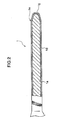
- FIG. 2 is a partially enlarged sectional view showing the inventive male terminal.
- FIG. 3 is a partially enlarged sectional view showing a state that the inventive male terminal and the female terminal are engaged with each other.
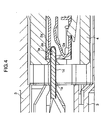
- FIG. 4 is an enlarged sectional view showing a state that the inventive male terminal is about to be disengaged from the female terminal.
- the male terminal 1 includes a box-shaped portion 1b constituting a terminal main body, and a male-type electric contact portion (male tab) 1a which extends in a forward direction of the male terminal 1 from the box-shaped portion 1b.
- the main body of the male terminal 1 is made of a material having a high conductivity such as copper.
- the male terminal 1 and a resinous housing 3 (see FIG. 3) for housing the male terminal 1 constitute a male connector.
- the female terminal 2 includes a box-shaped portion 2b.
- a contact spring piece 2a and a second contact piece 2a' which is opposed to the contact spring piece 2a are formed inside the box-shaped portion 2b at such a position as to tightly hold the male tab 1a therebetween.
- the female terminal 2 and a resinous housing 4 for housing the female terminal 2 constitute a female connector.
- the male tab 1a is rendered into contact with a female-type electric contact portion 2A comprised of the contact spring piece 2a and the second contact piece 2a' when the male terminal 1 is engaged with the female terminal 2.
- the terminals 1 and 2 are electrically communicable with each other.
- a predetermined region including a final contact site 1e of the male tab 1a of the male terminal 1 which is detached from the female terminal 2 at a final stage of detachment or disengagement is covered with a plating layer (arc discharge suppressive layer) 1c containing a metal having a high melting point.
- the predetermined region is sometimes referred to as "arc discharge suppressive site”.
- the lead end portion of the male terminal 1 corresponding to the final contact site 1e of the male tab 1a is covered with the arc discharge suppressive layer 1c (in the embodiment, Ni-W plating layer) containing tungsten as a metal having a high melting point.
- the remaining part of the male tab 1a other than the arc discharge suppressive site (in this embodiment, corresponding to the base end portion of the male tab 1a) is covered with a general-purpose plating layer 1d (in the embodiment, Sn plating layer) which is used for conventional terminals.
- a general-purpose plating layer 1d in the embodiment, Sn plating layer
- main contact site the remaining part of the male tab 1a other than the arc discharge suppressive site
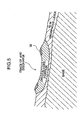
- FIG. 5 is a schematic sectional view.
- the base layer of the male tab 1a is covered with an Ni-W plating layer (arc discharge suppressive layer) in amorphous state with a crater-like insignificant trace of arc discharge being formed in the surface of the Ni-W plating layer.
- the crater-like portion includes an outer annular rib where condensed tungsten exists, and the remaining portion composed of crystallized structure. It is conceived that the crystallized portion is formed as a result of temporary melting of the amorphous Ni-W plating layer which follows cooling.
- the arc discharge suppressive layer 1c contains a metal, the arc discharge suppressive layer 1c has conductivity.
- the fact that the arc discharge suppressive layer 1c has conductivity is important in suppressing arc discharge.
- the portion of the male tab covered with the general-purpose plating layer (in this embodiment, Sn plating layer) is electrically communicated with the female-type electric contact portion 2A to a state where the male terminal is detached from the female terminal, the site of the male terminal in contact with the electric contact portion 2A is shifted from the site covered with the general-purpose plating layer 1d to the final contact site covered with the insulating member. Then, it is highly likely that arc discharge may occur during the shifting, thus failing to suppress occurrence of arc discharge. In view of the above, it is essential to provide the arc discharge suppressive layer 1c with conductivity that is sufficient to suppress occurrence of arc discharge. According to the embodiment of this invention, since the arc discharge suppressive layer 1c is a metallic plating layer, the aforementioned conductivity is secured.
- the arc discharge suppressive site is not specifically limited as far as the arc discharge suppressive site includes the final contact site 1e. However, it is desirable that the arc discharge suppressive site includes at least the following region, in addition to the final contact site 1e:
- a tongue end 1g or its vicinity in the example of FIGS. 2 and 4, the site 1e corresponds to the final contact site.
- the melting point of the high-melting metal is not lower than 1,550°C, preferably not lower than 1,600°C, furthermore preferably not lower than 1,700°C, and particularly preferably not lower than 2,500°C.
- examples of such a metal include molybdenum, platinum, and iridium, in addition to tungsten.
- the melting point of the high-melting metal is generally 4,000°C or lower.
- the high-melting metal include tungsten, molybdenum, platinum, and iridium (particularly, tungsten, platinum, and iridium).
- platinum and iridium can be used alone as a plating material.
- the metal having plating-layer formability is sometimes referred to as "plating metal" and to perform plating by utilizing the plating-layer formability of the plating metal.
- a metal having a melting point of not lower than 1,000°C and lower than 1,550°C is advantageous in plating with a high-melting metal (such as tungsten and molybdenum) without lowering the arc discharge suppressive ability of these high-melting metals, compared with a case that a metal having a melting point of lower than 1,000°C is used as the plating metal.
- a high-melting metal such as tungsten and molybdenum
- Examples of the metal having a melting point of not lower than 1,000°C and lower than 1,550°C include a metal which is classified into Group VIII of the periodic table of the elements such as iron, cobalt, and nickel.
- the plating metals are used alone or in combination of at least two kinds thereof.
- the particularly preferable plating metal includes cobalt and nickel.
- Cobalt and nickel have excellent corrosion resistance in addition to the advantage in plating with the high-melting metal.
- the arc discharge suppressive layer may be a plating layer of an alloy which is obtained by mixing tungsten or molybdenum with the plating metal.
- the arc discharge suppressive layer may be a complex plating layer in which tungsten, molybdenum, or an alloy thereof is dispersed in matrices of the plating metal.
- the ratio of the content of the high-melting metal to the total content of the compositions of the arc discharge suppressive layer is e.g. not smaller than 5 mass%, preferably not smaller than 20 mass%, furthermore preferably not smaller than 30 mass%, and particularly preferably not smaller than 40 mass%.
- the upper limit of the content of the high-melting metal (sum of the contents of tungsten and molybdenum) in the arc discharge suppressive layer is not specifically limited as far as a plating layer is formable.
- the upper limit of the high-melting metal content is generally 70 mass%, preferably 60 mass%, and particularly preferably 50 mass%.
- the arc discharge suppressive layer is a single layer.
- the thickness of the arc discharge suppressive layer can be optimally set depending on a potential difference right after the final stage of disengagement of terminals and a quantity of electric current flowing through the terminals.
- the thickness of the arc discharge suppressive layer is 3 ⁇ m or larger, preferably 5 ⁇ m or larger, and further preferably 10 ⁇ m or larger. Even if the thickness of the arc discharge suppressive layer is set exceedingly large, no further arc discharge suppressive effect is expected when the thickness exceeds a certain value.
- the thickness of the arc discharge suppressive layer is generally 30 ⁇ m or smaller, preferably 20 ⁇ m or smaller, and further preferably 15 ⁇ m or smaller.
- the manner of forming the arc discharge suppressive layer is not specifically limited.
- a known plating method (such as electrolytic plating and electroless plating) is usable to form the arc discharge suppressive layer.
- Electroless plating layer is more effective than electrolytic plating layer in suppressing arc discharge.
- the male terminal 1 and the female terminal 2 are in a completely engaged state, the male terminal 1 is in contact with the female terminal 2 at least at the main contact site other than the arc discharge suppressive site.
- the male tab 1a is in contact with the female terminal 2 not only at the lead end portion (arc discharge suppressive site) of the male tab 1a but also at the base end portion thereof. It is possible to cover the main contact site of the male tab 1a with the arc discharge suppressive layer (e.g. a plating layer containing at least one kind selected from the group consisting of tungsten, molybdenum, platinum, and iridium, as a high-melting metal).
- the arc discharge suppressive layer e.g. a plating layer containing at least one kind selected from the group consisting of tungsten, molybdenum, platinum, and iridium, as a high-melting metal.
- the main contact site of the male tab 1a with a layer composed of a material having a higher conductivity than the arc discharge suppressive layer, or a material having a low contact resistance than the arc discharge suppressive layer. Conductive reliability of the terminals can be secured by enhancing conductivity of the main contact site of the male tab 1a.
- the surface of the main contact site of the male tab 1a may be covered with a general-purpose plating layer (conventional plating layer) or may be left uncovered to directly expose the base of the male terminal 1 which is made of e.g. copper. It is preferable to cover the surface of the main contact site with a general-purpose plating layer. Covering the main contact site with a general-purpose plating layer not only enables to prevent corrosion of the base layer but also enables to enhance conductive reliability of the terminals because the surface of the general-purpose plating layer is relatively soft, which contributes to increase of the contact area of the main contact portion in contact with the counterpart terminal (female terminal).
- Examples of the general-purpose plating layer include a known plating layer used for a terminal, e.g., a plating layer made of gold, copper, tin, silver, nickel, or cobalt. In case of using nickel as a high-melting metal, it is often the case that a layer other than a nickel-plating layer is used as the general-purpose plating layer.
- the arc discharge suppressive layer 1c which is formed at the arc discharge suppressive site and the general-purpose plating layer 1d which is formed at the main contact site may be formed independently of each other in such a manner that the arc discharge suppressive layer 1c is not overlapped with the general-purpose plating layer 1d.
- the arc discharge suppressive layer and the general-purpose plating layer may be overlapped with each other as long as the final contact site 1e is covered with the arc discharge suppressive layer 1c.
- the general-purpose plating layer may constitute a base layer, and the arc discharge suppressive layer may partially be laid over the base layer in such a manner that the arc discharge suppressive layer covers the final contact site 1e.
- the arc discharge suppressive layer may constitute a base layer, and the general-purpose plating layer may partially be laid over the base layer (arc discharge suppressive layer) except the final contact site 1e.
- the configuration of the male tab 1a is not specifically limited.
- the male tab 1a can take a variety of forms such as plate-like, bar-like, or cylindrical shape.
- the base of the male terminal 1 is formed from a single piece made of a single material.
- a plurality of kinds of platings are applicable to the male terminal 1 by, for example, partially immersing the male terminal 1 in a plating solution (e.g. by immersing merely the lead end portion of the male tab 1a in a plating solution) or by a masking.
- the male terminal 1 can be produced in a simplified manner by preparing a lead end part on which the arc discharge suppressive layer 1c is formed, and a base end part on which a conductive plating layer is formed individually, and by assembling these parts together.
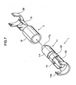
- FIG. 6 is a perspective view showing a state that a lead end part 11 and a main body part 12 are being assembled into the male terminal 1.
- FIG. 7 is a perspective view showing a state that the male terminal 1 in an assemble state is being engaged with the female terminal 2.
- the lead end part 11 constituting the male terminal 1 includes a cylindrical electric contact portion 11f covered with an arc discharge suppressive layer 11c, and a small-diametrical coupling shaft 11i extending rearward of the male terminal 1 from the electric contact portion 11f.
- the electric contact portion 11f and the coupling shaft 11i are integrally formed with each other.
- a tip end 11g of the electric contact portion 11f has a tapered shape (truncated conical shape).
- the main body part 12 includes a cylindrical electric contact portion 12f which corresponds to the main contact portion of the male terminal 1, a coupling-shaft holding portion 12i in the form of a barrel for tightly holding the coupling shaft 11i, and an electric-wire holding portion 12k in the form of a barrel for tightly holding an electric wire.
- the inner diameter of the main contact portion 12f has such a size as to receive the coupling shaft 11i of the lead end part 11.
- the outer diameter of the main contact portion 12f is substantially the same as the outer diameter of the electric contact portion 11f of the lead end part 11.
- the female terminal 2 includes a cylindrical electric contact portion 2f for fittingly receiving the electric contact portions 11f and 12f of the male terminal 1 substantially without a clearance, a conductive-wire holding portion 2i which is in the form of a barrel and is located behind the electric contact portion 2f for holding a conductive wire, and an insulating-layer holding portion 2k in the form of a barrel for tightly holding an insulating layer of a conductive wire.
- a similar arc discharge suppressive effect as in the embodiment can be obtained by covering the electric contact portion 11f of the lead end part 11 with an arc discharge suppressive layer. It is possible to cover the electric contact portion (main contact portion) 12f of the main body part 12 with an arc discharge suppressive layer in a similar manner as in the above embodiment. However, it is preferable to expose the base of the electric contact portion 12f without performing plating or to cover the electric contact portion 12f with a general-purpose plating layer.
- the lead end part 11 and the main body part 12 are assembled together into the terminal by various known methods such as engagement and caulking.
- the arc discharge suppressive layer may be formed on the female terminal in place of the male terminal.
- the arc discharge suppressive layer may be formed both on the male terminal and the female terminal.
- the arc discharge suppressive layer may be formed on the female terminal in a similar manner as the arc discharge suppressive layer is formed on the male terminal.
- the site of forming the arc discharge suppressive layer is not specifically limited as long as the arc discharge suppressive site includes a final contact site of the female terminal. For instance, in the case where the arc discharge suppressive layer is formed on the female terminal in the examples of FIGS.
- the arc discharge suppressive layer is formed on a region including a final contact site 2c (arc discharge suppressive site) which is in contact with the male terminal 1 at a final stage of detachment or disengagement. It may be possible to form the arc discharge suppressive layer on a main contact portion (e.g. the surface of the contact spring piece 2a) of the female terminal 2 as well as the final contact site 2e in a similar manner as the arc discharge suppressive layer is formed on the male terminal. However, it is desirable not to form the arc discharge suppressive layer on the main contact portion of the female terminal 2. It is possible to expose a base metal at a site of the main contact portion of the female terminal 2 in a similar manner as in the arrangement of the male terminal. Alternatively, the main contact portion of the female terminal 2 may be covered with a general-purpose plating layer.
- the inventive male (and/or female) terminal is covered with the arc discharge suppressive layer at the final contact site (arc discharge suppressive site) thereof.
- arc discharge suppressive site arc discharge suppressive site
- a high voltage e.g. about 36V
- a large electric current e.g. current of about 10A
- the male terminal is allowed to be engaged with and disengaged from the female terminal a plurality of number of times (e.g. thrice or more, preferably five times or more, furthermore preferably ten times or more) without occurrence of large arc discharge accompanied by glaring light.
- inventive terminal pair in a wire harness of an automobile is advantageous in suppressing occurrence of large arc discharge in detachment or disengagement of the terminals at the time of maintenance and checkup despite the fact that a high voltage is applied to the terminal pair.
- the inventive terminal pair may be applicable to a field where a low voltage (or low electric current) is applied. Namely, the inventive terminal pair may be used in a field where a low voltage is applied in order to secure a safety system, considering a possibility that a high voltage may be applied to the system due to occurrence of an operation failure or the like.
- Respective sets of the male tab 1a and the female-type electric contact portion 2A shown in FIGS. 1A through 4 were applied with a corresponding plating as shown in Table 1.
- the male tab 1a was tightly received in the female-type electric contact portion 2A until the male terminal 1 and the female terminal 2 were brought to a completely engaged state as shown in FIG. 3. Thereafter, the male terminal 1 was detached from the female terminal 2.
- the engagement and disengagement (detachment) were repeated a certain number of times while applying a voltage of 36V (current of 10A at the time of engagement) until a large arc discharge accompanied by glaring light occurred. Counted was the number of times during which the engagement and disengagement could carried on without causing large arc discharge.
- Ni ⁇ W 9 electrodes plating layer, Ni- W 46 electrolytic plating layer, and Co-W 46 electrolytic plating layer are alloy plating layers, respectively.
- a pair of arc discharge suppressive terminals electrically communicable with each other by engagement of the terminal pair has a feature that at least one of the terminal pair has a final contact site which is in contact with the counterpart terminal at a final stage of disengagement of the terminal pair, and that at least the final contact site is covered with a plating layer (arc discharge suppressive layer) containing a first metal (high-melting metal) having a melting point of 1,550°C or higher.
- the terminal pair contact with each other at a portion corresponding to a main contact site other than the arc discharge suppressive layer in a completely engaged state where the one of the terminal pair and the counterpart terminal are tightly engaged with each other, and the main contact site has a surface made of a material having a higher conductivity than the arc discharge suppressive layer, or a material having a lower contact resistance than the arc discharge suppressive layer.
- This arrangement provides improved conductive reliability.
- the high-melting metal includes tungsten, molybdenum, platinum, and iridium (particularly preferably, tungsten, platinum, and iridium).
- tungsten or molybdenum do not have plating-layer formability, it is necessary to perform plating with tungsten or molybdenum in combined use with a metal (plating metal) having plating-layer formability. It is recommendable to use a metal such as iron, cobalt, and nickel, as the plating metal because these metals have second-best arc discharge suppressive ability to the high-melting metal.
- the sum of the contents of tungsten and molybdenum ranges from 5 to 70 mass% with respect to the total content of the compositions of the arc discharge suppressive layer.
- the thickness of the arc discharge suppressive layer is set at 3 ⁇ m or larger.
Landscapes
- Connector Housings Or Holding Contact Members (AREA)
Abstract
Description

Claims (9)
- A pair of arc discharge suppressive terminals electrically communicable with each other by engagement of the terminal pair, wherein at least one of the terminal pair has a final contact site which is in contact with the counterpart terminal at a final stage of disengagement of the terminal pair, and at least the final contact site is covered with an arc discharge suppressive layer containing a first metal having a melting point of 1,550°C or higher.
- The arc discharge suppressive terminal pair according to claim 1, wherein said terminal pair contact with each other at a portion corresponding to a main contact site other than the arc discharge suppressive layer in a completely engaged state where the one of the terminal pair and the counterpart terminal are tightly engaged with each other, and the main contact site has a surface made of a material having a higher conductivity than the arc discharge suppressive layer.
- The arc discharge suppressive terminal pair according to claim 1, wherein said terminal pair contact with each other at a portion corresponding to a main contact site other than the arc discharge suppressive layer in a completely engaged state where the one of the terminal pair and the counterpart terminal are tightly engaged with each other, and the main contact site has a surface made of a material having a lower contact resistance than the arc discharge suppressive layer.
- The arc discharge suppressive terminal pair according to any one of claims 1 through 3, wherein the first metal is at least one kind selected from the group consisting of tungsten, molybdenum, platinum, and iridium.
- The arc discharge suppressive terminal pair according to any one of claims 1 through 3, wherein the first metal is at least one kind selected from the group consisting of tungsten, platinum, and iridium.
- The arc discharge suppressive terminal pair according to claim 4, wherein the arc discharge suppressive layer includes tungsten and/or molybdenum, and a second metal having plating layer formability.
- The arc discharge suppressive terminal pair according to claim 6, wherein the sum of the contents of tungsten and molybdenum ranges from 5 to 70 mass% with respect to the total content of compositions of the arc discharge suppressive layer.
- The arc discharge suppressive terminal pair according to claim 6 or 7, wherein the second metal is at least one kind selected from the group consisting of iron, cobalt, and nickel.
- The arc discharge suppressive terminal pair according to any one of claims 1 through 8, wherein the arc discharge suppressive layer has a thickness of 3 µm or larger.
Applications Claiming Priority (4)
| Application Number | Priority Date | Filing Date | Title |
|---|---|---|---|
| JP2002049697 | 2002-02-26 | ||
| JP2002049697 | 2002-02-26 | ||
| JP2002231300 | 2002-08-08 | ||
| JP2002231300A JP2003323929A (en) | 2002-02-26 | 2002-08-08 | Arc resistant terminal pair |
Publications (3)
| Publication Number | Publication Date |
|---|---|
| EP1339137A2 true EP1339137A2 (en) | 2003-08-27 |
| EP1339137A3 EP1339137A3 (en) | 2004-07-07 |
| EP1339137B1 EP1339137B1 (en) | 2006-12-20 |
Family
ID=27667561
Family Applications (1)
| Application Number | Title | Priority Date | Filing Date |
|---|---|---|---|
| EP03004228A Expired - Lifetime EP1339137B1 (en) | 2002-02-26 | 2003-02-25 | Arc discharge suppressive terminal pair |
Country Status (4)
| Country | Link |
|---|---|
| US (1) | US6860746B2 (en) |
| EP (1) | EP1339137B1 (en) |
| JP (1) | JP2003323929A (en) |
| DE (1) | DE60310464T8 (en) |
Families Citing this family (20)
| Publication number | Priority date | Publication date | Assignee | Title |
|---|---|---|---|---|
| DE10317330B4 (en) * | 2002-04-15 | 2013-12-24 | Autonetworks Technologies, Ltd. | Arc-resistant terminal, use thereof for an arc-resistant terminal pair, for a connector, for a connection box, for a breaker device or the like and for a motor vehicle and a motor |
| JP2006256448A (en) * | 2005-03-16 | 2006-09-28 | Tyco Electronics Amp Kk | Automobile connector assembly |
| US20070221591A1 (en) * | 2006-03-24 | 2007-09-27 | Yang-Yuan Hsu | Wedged sliding trough structure |
| JP2008108675A (en) * | 2006-10-27 | 2008-05-08 | Toshiba Corp | plug |
| US7467960B1 (en) * | 2007-07-23 | 2008-12-23 | Hon Hai Precision Ind. Co., Ltd. | Receptacle connector with arcing reducing structure |
| JP5246503B2 (en) * | 2009-02-23 | 2013-07-24 | 住友電装株式会社 | Terminal fitting |
| US8226425B2 (en) * | 2009-07-31 | 2012-07-24 | American Power Conversion Corporation | Sparkless electrical connector |
| JP2011113679A (en) * | 2009-11-24 | 2011-06-09 | Panasonic Electric Works Co Ltd | Blade rest member and receptacle with this |
| JP2011113680A (en) * | 2009-11-24 | 2011-06-09 | Panasonic Electric Works Co Ltd | Screw terminal and receptacle with this |
| US8619395B2 (en) | 2010-03-12 | 2013-12-31 | Arc Suppression Technologies, Llc | Two terminal arc suppressor |
| US8545275B2 (en) * | 2010-04-07 | 2013-10-01 | Alltop Electronics (Suzhou) Ltd. | Electrical connector with touch-safety contact structures |
| FR3009445B1 (en) * | 2013-07-31 | 2017-03-31 | Hypertac Sa | CONTACT MEMBER BETWEEN A SUPPORT AND A DEVICE AND ELECTRICAL CONNECTOR COMPRISING SUCH A CONTACT MEMBER |
| KR101734716B1 (en) | 2015-12-11 | 2017-05-11 | 현대자동차주식회사 | High voltage connector for vehicle |
| EP3211722B1 (en) * | 2016-02-23 | 2020-04-22 | TE Connectivity Germany GmbH | Contact stud and contact assembly in particular for car technology |
| US20190273341A1 (en) * | 2018-03-01 | 2019-09-05 | Dell Products L.P. | High Speed Connector |
| JP2020047500A (en) * | 2018-09-20 | 2020-03-26 | 矢崎総業株式会社 | Terminal mating structure |
| CN111403937A (en) * | 2020-03-24 | 2020-07-10 | 东莞立德精密工业有限公司 | Metal terminal and manufacturing method thereof |
| CN114069301B (en) * | 2021-12-28 | 2025-02-18 | 海固科技(苏州)有限公司 | An electrical connector and a female end plug thereof |
| CN217485753U (en) * | 2022-05-30 | 2022-09-23 | 泰科电子科技(苏州工业园区)有限公司 | Connecting terminal, connecting terminal assembly, cable assembly and charging seat |
| WO2024202237A1 (en) * | 2023-03-30 | 2024-10-03 | Jx金属株式会社 | Metal material and sliding component |
Family Cites Families (14)
| Publication number | Priority date | Publication date | Assignee | Title |
|---|---|---|---|---|
| JPS57118312A (en) * | 1981-01-14 | 1982-07-23 | Tokyo Shibaura Electric Co | Electric contactor |
| US4752334A (en) * | 1983-12-13 | 1988-06-21 | Scm Metal Products Inc. | Dispersion strengthened metal composites |
| US4999336A (en) * | 1983-12-13 | 1991-03-12 | Scm Metal Products, Inc. | Dispersion strengthened metal composites |
| US4747783A (en) * | 1986-10-28 | 1988-05-31 | International Business Machines Corporation | Resistive pin for printed circuit card connector |
| JPS63298927A (en) * | 1987-05-28 | 1988-12-06 | Nec Corp | Electric contact |
| US5139891A (en) * | 1991-07-01 | 1992-08-18 | Olin Corporation | Palladium alloys having utility in electrical applications |
| US5236789A (en) * | 1991-07-01 | 1993-08-17 | Olin Corporation | Palladium alloys having utility in electrical applications |
| US5208978A (en) * | 1992-05-07 | 1993-05-11 | Molex Incorporated | Method of fabricating an electrical terminal pin |
| JPH07335329A (en) * | 1994-06-13 | 1995-12-22 | Fujitsu Denso Ltd | Rush current limiting connector |
| JPH08171954A (en) * | 1994-12-16 | 1996-07-02 | World Metal:Kk | Contact point material and contact point member using it |
| JP2001035578A (en) * | 1999-05-14 | 2001-02-09 | Mitsubishi Electric Corp | Test socket for electronic circuit device and method of manufacturing the same |
| JP2001266986A (en) * | 2000-03-24 | 2001-09-28 | Fujikura Ltd | Male terminal and connector and electrical connection structure using the same |
| JP2001266985A (en) | 2000-03-24 | 2001-09-28 | Fujikura Ltd | Male terminal and connector and electrical connection structure using the same |
| US6537091B2 (en) * | 2000-11-28 | 2003-03-25 | Autonetworks Technologies, Ltd. | Arc discharge suppressive terminal, method for producing such terminal, and arc discharge suppressive connector |
-
2002
- 2002-08-08 JP JP2002231300A patent/JP2003323929A/en active Pending
-
2003
- 2003-02-25 DE DE60310464T patent/DE60310464T8/en active Active
- 2003-02-25 EP EP03004228A patent/EP1339137B1/en not_active Expired - Lifetime
- 2003-02-25 US US10/372,128 patent/US6860746B2/en not_active Expired - Fee Related
Non-Patent Citations (1)
| Title |
|---|
| None |
Also Published As
| Publication number | Publication date |
|---|---|
| DE60310464T2 (en) | 2007-09-27 |
| JP2003323929A (en) | 2003-11-14 |
| DE60310464D1 (en) | 2007-02-01 |
| US20030176093A1 (en) | 2003-09-18 |
| US6860746B2 (en) | 2005-03-01 |
| EP1339137B1 (en) | 2006-12-20 |
| EP1339137A3 (en) | 2004-07-07 |
| DE60310464T8 (en) | 2008-02-21 |
Similar Documents
| Publication | Publication Date | Title |
|---|---|---|
| US6860746B2 (en) | Arc discharge suppressive terminal pair | |
| JP3980463B2 (en) | Arc-resistant terminals, arc-proof terminal pairs, and automotive connectors | |
| EP2434584B1 (en) | Connector terminal | |
| JP6616058B2 (en) | Terminal and aluminum wire connection structure of the terminal | |
| US20060025024A1 (en) | Electrical connector | |
| WO2009102074A1 (en) | Press-clamping terminal and crimped structure using the press-clamping terminal | |
| WO2006077827A1 (en) | Press-fit terminal, press-fit terminal manufacturing method and structure for connecting press-fit terminal and circuit board | |
| US9954297B2 (en) | Terminal fitting and connector | |
| US10218102B2 (en) | Terminal fitting and connector | |
| JP2004006070A (en) | Female terminal | |
| US6607392B2 (en) | Ground joint connector | |
| EP1229609B1 (en) | ARC discharge suppressive connector | |
| US20190036237A1 (en) | Electric wire with terminal | |
| JP2003031333A (en) | Terminal manufacturing method | |
| DE102010042526A1 (en) | contact element | |
| US20190036238A1 (en) | Electric Wire With Terminal | |
| CN114402487B (en) | Pin terminal, connector, wire harness with connector, and control unit | |
| JP7223332B2 (en) | Pin terminals, connectors, wire harnesses with connectors, and control units | |
| JP7226210B2 (en) | Pin terminals, connectors, wire harnesses with connectors, and control units | |
| CN110350339B (en) | Conductive terminal, manufacturing method thereof and electric connector | |
| JP3999158B2 (en) | Arc-resistant terminals, arc-proof terminal pairs, and automotive connectors | |
| KR20240033675A (en) | Terminal socket, terminal pin, terminal system, and terminal assembly | |
| WO2021054106A1 (en) | Pin terminal, connector, wire harness equipped with connector, and control unit | |
| WO2021054109A1 (en) | Pin terminal, connector, wire harness with connector, and control unit |
Legal Events
| Date | Code | Title | Description |
|---|---|---|---|
| PUAI | Public reference made under article 153(3) epc to a published international application that has entered the european phase |
Free format text: ORIGINAL CODE: 0009012 |
|
| AK | Designated contracting states |
Designated state(s): AT BE BG CH CY CZ DE DK EE ES FI FR GB GR HU IE IT LI LU MC NL PT SE SI SK TR |
|
| AX | Request for extension of the european patent |
Extension state: AL LT LV MK RO |
|
| PUAL | Search report despatched |
Free format text: ORIGINAL CODE: 0009013 |
|
| AK | Designated contracting states |
Kind code of ref document: A3 Designated state(s): AT BE BG CH CY CZ DE DK EE ES FI FR GB GR HU IE IT LI LU MC NL PT SE SI SK TR |
|
| AX | Request for extension of the european patent |
Extension state: AL LT LV MK RO |
|
| 17P | Request for examination filed |
Effective date: 20040810 |
|
| 17Q | First examination report despatched |
Effective date: 20041103 |
|
| AKX | Designation fees paid |
Designated state(s): DE |
|
| GRAP | Despatch of communication of intention to grant a patent |
Free format text: ORIGINAL CODE: EPIDOSNIGR1 |
|
| GRAS | Grant fee paid |
Free format text: ORIGINAL CODE: EPIDOSNIGR3 |
|
| RIN1 | Information on inventor provided before grant (corrected) |
Inventor name: MASAHIRO, SHIBATA,SUMITOMO ELECTRIC INDUSTR., LTD Inventor name: TSUJI, YOSHITSUGU,AUTONETWORKS TECHNOLOGIES, LTD. Inventor name: KIMURA, ATSUSHI,SUMITOMO ELECTRIC INDUSTR., LTD Inventor name: HAYASHI, NORIKI,SUMITOMO ELECTRIC INDUSTR., LTD Inventor name: HIRAI, HIROKI,AUTONETWORKS TECHNOLOGIES, LTD. Inventor name: YAGI NARITO,SUMITOMO ELECTRIC INDUSTR., LTD Inventor name: TAKANO, SATOSHI,SUMITOMO ELECTRIC INDUSTRIES, LTD Inventor name: OTA, KOUJI,AUTONETWORKS TECHNOLOGIES, LTD. Inventor name: KANDA, MASAHIKO |
|
| GRAA | (expected) grant |
Free format text: ORIGINAL CODE: 0009210 |
|
| AK | Designated contracting states |
Kind code of ref document: B1 Designated state(s): DE |
|
| REF | Corresponds to: |
Ref document number: 60310464 Country of ref document: DE Date of ref document: 20070201 Kind code of ref document: P |
|
| PLBE | No opposition filed within time limit |
Free format text: ORIGINAL CODE: 0009261 |
|
| STAA | Information on the status of an ep patent application or granted ep patent |
Free format text: STATUS: NO OPPOSITION FILED WITHIN TIME LIMIT |
|
| 26N | No opposition filed |
Effective date: 20070921 |
|
| PGFP | Annual fee paid to national office [announced via postgrant information from national office to epo] |
Ref country code: DE Payment date: 20130220 Year of fee payment: 11 |
|
| REG | Reference to a national code |
Ref country code: DE Ref legal event code: R119 Ref document number: 60310464 Country of ref document: DE |
|
| REG | Reference to a national code |
Ref country code: DE Ref legal event code: R119 Ref document number: 60310464 Country of ref document: DE Effective date: 20140902 |
|
| PG25 | Lapsed in a contracting state [announced via postgrant information from national office to epo] |
Ref country code: DE Free format text: LAPSE BECAUSE OF NON-PAYMENT OF DUE FEES Effective date: 20140902 |