EP1339077A2 - Capacitor for low voltage - Google Patents
Capacitor for low voltage Download PDFInfo
- Publication number
- EP1339077A2 EP1339077A2 EP03000083A EP03000083A EP1339077A2 EP 1339077 A2 EP1339077 A2 EP 1339077A2 EP 03000083 A EP03000083 A EP 03000083A EP 03000083 A EP03000083 A EP 03000083A EP 1339077 A2 EP1339077 A2 EP 1339077A2
- Authority
- EP
- European Patent Office
- Prior art keywords
- anode
- cathode
- capacitor
- layer
- terminal
- Prior art date
- Legal status (The legal status is an assumption and is not a legal conclusion. Google has not performed a legal analysis and makes no representation as to the accuracy of the status listed.)
- Withdrawn
Links
Images




Classifications
-
- H—ELECTRICITY
- H01—ELECTRIC ELEMENTS
- H01G—CAPACITORS; CAPACITORS, RECTIFIERS, DETECTORS, SWITCHING DEVICES, LIGHT-SENSITIVE OR TEMPERATURE-SENSITIVE DEVICES OF THE ELECTROLYTIC TYPE
- H01G2/00—Details of capacitors not covered by a single one of groups H01G4/00-H01G11/00
- H01G2/02—Mountings
- H01G2/04—Mountings specially adapted for mounting on a chassis
-
- H—ELECTRICITY
- H01—ELECTRIC ELEMENTS
- H01G—CAPACITORS; CAPACITORS, RECTIFIERS, DETECTORS, SWITCHING DEVICES, LIGHT-SENSITIVE OR TEMPERATURE-SENSITIVE DEVICES OF THE ELECTROLYTIC TYPE
- H01G4/00—Fixed capacitors; Processes of their manufacture
- H01G4/38—Multiple capacitors, i.e. structural combinations of fixed capacitors
-
- H—ELECTRICITY
- H01—ELECTRIC ELEMENTS
- H01G—CAPACITORS; CAPACITORS, RECTIFIERS, DETECTORS, SWITCHING DEVICES, LIGHT-SENSITIVE OR TEMPERATURE-SENSITIVE DEVICES OF THE ELECTROLYTIC TYPE
- H01G9/00—Electrolytic capacitors, rectifiers, detectors, switching devices, light-sensitive or temperature-sensitive devices; Processes of their manufacture
- H01G9/004—Details
- H01G9/008—Terminals
-
- H—ELECTRICITY
- H01—ELECTRIC ELEMENTS
- H01G—CAPACITORS; CAPACITORS, RECTIFIERS, DETECTORS, SWITCHING DEVICES, LIGHT-SENSITIVE OR TEMPERATURE-SENSITIVE DEVICES OF THE ELECTROLYTIC TYPE
- H01G9/00—Electrolytic capacitors, rectifiers, detectors, switching devices, light-sensitive or temperature-sensitive devices; Processes of their manufacture
- H01G9/004—Details
- H01G9/14—Structural combinations or circuits for modifying, or compensating for, electric characteristics of electrolytic capacitors
-
- Y—GENERAL TAGGING OF NEW TECHNOLOGICAL DEVELOPMENTS; GENERAL TAGGING OF CROSS-SECTIONAL TECHNOLOGIES SPANNING OVER SEVERAL SECTIONS OF THE IPC; TECHNICAL SUBJECTS COVERED BY FORMER USPC CROSS-REFERENCE ART COLLECTIONS [XRACs] AND DIGESTS
- Y02—TECHNOLOGIES OR APPLICATIONS FOR MITIGATION OR ADAPTATION AGAINST CLIMATE CHANGE
- Y02T—CLIMATE CHANGE MITIGATION TECHNOLOGIES RELATED TO TRANSPORTATION
- Y02T10/00—Road transport of goods or passengers
- Y02T10/60—Other road transportation technologies with climate change mitigation effect
- Y02T10/70—Energy storage systems for electromobility, e.g. batteries
Definitions
- the present invention relates to an electric device that requires high power consumption with a comparatively low voltage, such as a battery driven motor.
- the invention allows to suppress the surge voltage during switching by lowering the wiring inductance in the connection device of a capacitor, enabling to use low-loss high-efficient semiconductor devices with low-withstand voltage to thereby achieve a small-sized low-cost and high-performance electric device.
- a method of improving the frequency response of an electrolytic capacitor connected to an electric device and suppressing the surge voltage has been discussed, for example, in Japanese Patent Laid-open No. Hei 6-275476.
- the method takes on the following construction illustrated in Figs. 1A and 1B of the specification.
- tabs for taking out an anode lead and a cathode lead which are installed on the upper part of a capacitor element made up with laminated plates, are separately tied up in a bundle and attached each to integrated leads.
- the integrated leads are coupled to external connection terminals through anode and cathode connection terminals for connecting to a sealing plate to seal the case.
- to form the integrated leads and the anode and cathode connection terminals into parallel broad plates will achieve a sufficient lowering of the internal inductance inside the case of the electrolytic capacitor.
- the spacing between the parts attached to the anode foil and cathode foil of the folder tabs is widely set, and the length of the connection devices extended to the upper electrode terminals is also set long.
- the spacing between the parts attached to the anode foil and cathode foil of the folder tabs is narrowed, and the length of the connection devices extended to the upper electrode terminals is shortened, thus achieving remarkably reduced inductance.
- Total inductance Inductance inside a capacitor + Inductance of the power wiring for connecting the capacitor to an electric device + Inductance inside the electric device
- the above examples 1 and 2 introduced in the related art are the invention relating to the lowering of the inductance inside the capacitor in the first term on the right side of the above expression.
- For the reduction of the inductance inside the electric device in the third term there have been various inventions related to individual electric devices.
- these conventional techniques cannot lower the inductance of the power wiring for connecting the capacitor to the electric device in the second term of the above expression, which is a limit in regard to improving the frequency response and suppressing the surge voltage.
- the present invention has been made in view of the above circumstances, and the invention intends to realize the reduction of the total inductance for the use of a low-voltage device by greatly reducing the inductance of the power wiring parts that connect an electrolytic capacitor to an electric device in order to improve the frequency response and suppress the surge voltage of the electric device. Further it is an object of the invention to allow the use of low-loss high-efficient semiconductor devices with a low-withstand voltage, thereby providing a small-sized low-cost and high-performance electric device.
- the terminals are placed close to the external terminals of the case.
- a laminated wiring in which two broad flat plates with an insulating layer sandwiched in-between are overlapped. Being placed in proximity to the external terminals of the case, the laminated wiring increases the suppression effect of inductance to a great extent, thus achieving the reduction of inductance of the power wiring parts.
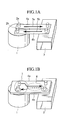
- Fig. 1A and Fig. 1B comparably illustrate two types of power wirings that connect electrolytic capacitors to electric devices.
- an anode electrode terminal 2a and a cathode electrode terminal 2b that are attached to a case 1 of an electrolytic capacitor are connected to an electric device 3 by means of a power wiring 4a on the anode side and a power wiring 4b on the cathode side.
- the power wirings 4a and 4b are made of narrow conductive plates, and are arranged in parallel with a spacing substantially equal to the distance between the electrode terminals 2a and 2b.
- a charge/discharge current 5a of the capacitor that flows through the power wiring 4a on the anode side and a charge/discharge current 5b of the capacitor that flows through the power wiring 4b on the cathode side do not have an overlapped area. Accordingly, the to-and fro currents (5a, 5b) induces a strong magnetic field in the surrounding space, whereby the power wirings 4a, 4b will possess large wiring inductances.
- this embodiment adopts a method as illustrated in Fig. 1B as a measure to reduce the inductance.
- Both the power wiring 4a on the anode side and the power wiring 4b on the cathode side employ wide conductive plates, and both plates are arranged in parallel to overlap each other. Because of this construction, the currents 5a and 5b flowing through the power wirings come close and overlap each other in a middle area 6 between the electric device 3 and the case 1 of the electrolytic capacitor, which suppresses the magnetic field induced on the surrounding space almost to zero, thus reducing the inductance.
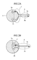
- an area 7 near the electrolytic capacitor of the power wirings 4a, 4b needs to be small.
- the electrode terminals 2a and 2b are arranged to come close as illustrated in Fig 2A.
- the area 7 where the currents does not overlap is made small in comparison to the case in Fig. 2A, which will reduce the inductance of the power wirings to a great extent.
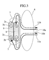
- a first capacitor 8 and a second capacitor 9 of a small capacitance are arranged adjacently with the anode electrode terminal 2a and the cathode electrode terminal 2b put in reverse polarity.
- the capacitances of the two capacitors 8, 9 are set equal.
- FIG. 4A On the upper surface of a sealing plate 12 of an electrolytic capacitor are mounted an anode electrode terminal 2a and a cathode electrode terminal 2b of L-letter shaped plate.
- a broad plate-formed anode power wiring 4a and a cathode power wiring 4b are used so as to sandwich an insulating sheet 13 in-between.
- the power wirings 4a , 4b are fastened to the electrode terminals 2a, 2b with screws 14. Accordingly, as shown in Fig.
- a high current has to be flown through the long cylindrical electrode terminals, and the diameter of the electrode was needed to be sufficiently large to prevent increase of the current density. This gave a limit to placing the electrode terminals 2 adjacently.
- the first embodiment employs broad conductive plates for the electrode terminals, it is possible to prevent increase of the current density in the electrode terminals, and to decrease the thickness of the conductive plates. Therefore, it is possible to place the electrode terminals sufficiently close.
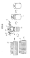
- an anode tab connection plate 17a and a cathode tab connection plate 17b each have two electrode terminals 2a and 2b mounted thereon.
- the tab connection plates 17a, 17b are integrally molded using resin into a sealing plate 12.
- the anode electrode terminals 2a and the cathode electrode terminals 2b are alternately projected in a slightly dislocated manner.
- anode tab connection plate 17a and the cathode tab connection plate 17b are exposed with a partition plate 18 put in-between.
- a broad plate-formed anode power wiring 4a and a cathode power wiring 4b are used so as to sandwich the insulating sheet 13 in-between. According to this embodiment, since the currents flowing through almost all the areas on the power wirings overlap except for a limited area between the electrode terminal 2b and the cathode power wiring 4b near the capacitor connection area, a significant reduction of the inductance of the power wiring 4 can be realized.
- An anode foil 19a and a cathode foil 19b each have conductive foil folder tabs 20 stuck thereon in a manner that the upper parts of the tabs 20 protrude, and then electrolyte layers are put in-between and wound in a roll to form a winding 21.
- the upper parts of the folder tabs 20 that protrude from the anode foil 19a and the cathode foil 19b are separately bundled.
- the non-molded exposed portions of anode and cathode tab connection plates 17a and 17b are provided on the lower surface of a sealing plate 12, and on both sides of the partition plate 18.
- the bundled folder tabs 20 are connected to these exposed portions, and are fastened by tightening stops 22 with bolts 23 and nuts 24.
- the winding 21 is housed in the case 1, which is sealed by the sealing plate 12, and the electrolytic capacitor is completed. According to this embodiment, even if the electrode terminals 2 are placed adjacently on the upper surface of the sealing plate 12, the folder tabs 20 can easily be mounted, and the manufacturing process becomes simple, which makes it possible to provide a low-cost and high-performance electrolytic capacitor.
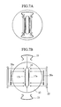
- FIG. 7A and 7B A fifth embodiment of this invention will be described with Figs. 7A and 7B.
- the folder tabs 20 are connected to the tab connection plates 17 on the lower surface of the sealing plate 12 in the fourth embodiment, tightening the stops 22 with the bolts 23 and the nuts 24 fastens the folder tabs 20.
- the folder tabs 20 are pressed to the tab connection plates 17 on both sides of the partition plate 18 by the stops 22, and then fixed under pressure by spring clips 25, thereby eliminating the thread fastening work and still more improving the workability.
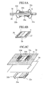
- a chip capacitor 26 has anode electrode pads 27 and cathode electrode pads 28 arranged along the facing sides on the upper surface thereof.
- a printed board has an anode side 29 and a cathode side 30 that are composed of a conductive plate, which are bonded as a solid plane.
- the anode side 29 and cathode side 30 each have the same number of via holes 31 as that of the anode electrode pads 27 and cathode electrode pads 28 on the upper side of the chip capacitor 26.
- the via holes are adjacently provided and connected to the opposite side.
- a first chip capacitor 26a and a second chip capacitor 26b are pasted each at the same positions on the anode side 29 and the cathode side 30 of the printed board.
- the first chip capacitor 26a is connected directly to the anode side 29, but through the via holes 31 to the cathode side 30 of the printed board.
- the second chip capacitor 26b is connected directly to the cathode side 30, but through the via holes 31 to the anode side 29 of the printed board.
- a first current running through the first chip capacitor 26a flows through a wire lead 32b, the first chip capacitor 26a, a wire lead 32a, and the cathode side 30 of the printed board in this order.
- a second current running through the second chip capacitor 26b flows through the anode side 29 of the printed board, a wire lead 32c, the second chip capacitor 26b, and a wire lead 32d in this order.
- the first current running through the first chip capacitor 26a and the second current running through the second chip capacitor 26b run in the opposite direction and overlap in the vertical direction to the printed board; therefore, a sharp reduction of the inductance becomes possible.
- FIG. 9 illustrates three-phase two-level IGBT inverter.
- the alternate power supplied from a commercial ac power source 33 after passing through a diode rectifier 35 using a rectifying diode 34, is stored in an electrolytic capacitor 36 as a dc power.
- the dc power is again inverted into an ac power of a variable frequency by means of a dc/ac inverter 39 using an IGBT 37 and a freewheeling diode 38, thus driving an ac motor 40.
- the inductance of a power wiring 4 that connects the electrolytic capacitor 36 to the dc/ac inverter 39 is large, a high surge voltage is applied to the IGBT 37 during the off operation of the IGBT 37, which possibly gives a risk that destroys the IGBT 37.
- the use of the electrolytic capacitor 36 of the present invention will suppress the surge voltage to prevent destruction of the device.
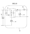
- FIG. 10 illustrates a switching power supply using one-transistor forward converter.
- a high-voltage dc power stored in the electrolytic capacitor 36 is converted into a pulse current by turning on and off a MOSFET 41 on the primary side, which is supplied to the primary side of a high frequency transformer 42 . Then, a low-voltage pulse is generated on the secondary side of the high frequency transformer 42 .
- the high-voltage dc power is converted into a low-voltage dc power by rectifying a current flowing through the secondary side by the pulse voltage generated by means of a MOSFET 43 on the secondary side and a reactor 44 .
- the inductance of the power wiring 4 that connects the electrolytic capacitor 36 to the switching power supply 45 is high, the high frequency characteristics are deteriorated.
- the use of the electrolytic capacitor 36 of this invention will improve the frequency characteristic.
- FIG. 11 illustrates a construction of a drive system in a vehicle.
- reference numeral 46 denotes a motor, 47 a power conversion device; 48 a dc power supply; 36 the electrolytic capacitor; 49 an output wiring; 50 the vehicle; 51 a control device; 52 a transmission gear; 53 an engine; 54a , 54b , 54c , 54d a wheel; and 55 a signal terminal.
- the signal terminal 55 receives signals relating to the driving state of the vehicle, and the commands from the driver, such as start, acceleration, deceleration, stop, etc.
- the control device 51 transmits a control signal to the power conversion device 47 on the basis of information received from the signal terminal 55, and drives the motor 46 by the power from the dc power supply 48 .
- the motor 46 transfers the torque to the engine shaft, and is able to drive the wheels through the transmission gear 52. That is, the drive system in Fig. 11 allows the motor 46 to drive the wheels 54a through 54d when the engine 53 is in stop, and also to assist a torque when the engine 53 is operative. It is also possible to make the engine 53 drive the motor 46, and to convert an ac power generated by the motor 46 into a dc power by means of the power conversion device 47 to thereby charge the dc power into the dc power supply 48.
- the electrolytic capacitor 36 is disposed between the dc power supply 48 and the power conversion device 47, whereby the power is stored temporarily to increase the capacity of the dc power supply 48 apparently and to improve the transient response of the dc power supply 48 .
- the motor 46 since a high torque is required during driving the wheels only by the motor 46 or assisting the torque, and the dc power supply is a low-voltage power supply such as a storage battery, the motor 46 has to be driven by a low-voltage high-current power. Accordingly, it is essential that the power conversion device 47 adopts a semiconductor device of a low resistance that dissipates little power in a high current. However, the semiconductor device of a low resistance is vulnerable to a surge excessive voltage, and an efficient power conversion device has to provide a surge voltage suppression mechanism. The adoption of the electrolytic capacitor 36 of this invention will suppress the surge voltage, which makes it possible to provide a vehicle having a high-efficient drive system.
- the invention achieves an electrolytic capacitor having an excellent frequency response, which enables to suppress a surge voltage.
Landscapes
- Engineering & Computer Science (AREA)
- Power Engineering (AREA)
- Microelectronics & Electronic Packaging (AREA)
- Manufacturing & Machinery (AREA)
- Inverter Devices (AREA)
- Power Conversion In General (AREA)
Abstract
Description
The method takes on the following construction illustrated in Figs. 1A and 1B of the specification. In the method, tabs for taking out an anode lead and a cathode lead, which are installed on the upper part of a capacitor element made up with laminated plates, are separately tied up in a bundle and attached each to integrated leads. The integrated leads are coupled to external connection terminals through anode and cathode connection terminals for connecting to a sealing plate to seal the case. In this case, to form the integrated leads and the anode and cathode connection terminals into parallel broad plates will achieve a sufficient lowering of the internal inductance inside the case of the electrolytic capacitor.
In contrast to this, this embodiment adopts a method as illustrated in Fig. 1B as a measure to reduce the inductance. Both the
Claims (18)
- A capacitor comprising:wherein flat plates are used for the power wirings, the flat plates being placed in parallel.an anode foil (19a) and a cathode foil (19b);an electrolyte layer placed between the anode foil and the cathode foil;a case (1) that houses the anode foil, the cathode foil, and the electrolyte layer;an anode terminal 2a and a cathode terminal 2b that are attached on the outside of the case;at least one tab 17a, 17b, 20 that connects each of the anode foil and the cathode foil to the anode terminal andthe cathode terminal; andpower wirings (4a, 4b) that are connected to the anode terminal and the cathode terminal;
- A capacitor comprising:wherein flat plates are used for the power wirings, the flat plates being placed in parallel.an anode layer (19a) and a cathode layer (19b);a dielectric layer placed between the anode layer and, the cathode layer;a case (1) that houses the anode layer, the cathode layer, and the dielectric layer;an anode terminal (2a) and a cathode terminal (2b) that are attached on the outside of the case;at least one tab (17a, 17b, 20) that connects each of the anode layer and the cathode layer to the anode terminal andthe cathode terminal; andpower wirings (4a, 4b) that are connected to the anode terminal and the cathode terminal;
- The capacitor as claimed in Claim 1, wherein the flat plates are used for the anode terminal and the cathode terminal.
- The capacitor as claimed in Claim 3, wherein the anode terminal and the cathode terminal are placed in parallel.
- A capacitor comprising:wherein the pairs of terminals are placed alternately in reverse direction, and the flat plates are used for the power wirings.an anode foil (19a) and a cathode foil (19b);an electrolyte layer placed between the anode foil and the cathode foil;a case (1) that houses the anode foil, the cathode foil, and the electrolyte layer;a pair of anode terminals (2a) and a pair of cathode terminals (2b) that are attached on the outside of the case;at least one tab (17a, 17b) that connects each of the anode foil and the cathode foil to the anode terminals and the cathode terminals; andpower wirings (4a, 4b) that are connected to the anode terminal and the cathode terminal;
- The capacitor as claimed in Claim 5, wherein the capacitor is used in the number of a plurality of pieces.
- A capacitor comprising:wherein the pairs of terminals are placed alternately in reverse direction, and the flat plates are used for the power wirings.an anode layer (19a) and a cathode layer (19b);a dielectric layer placed between the anode layer and the cathode layer;a case (1) that houses the anode layer, the cathode layer, and the dielectric layer;a pair of anode terminals (2a) and a pair of cathode terminals (2b) that are attached on the outside of the case;at least one tab (17a, 17b, 20) that connects each of the anode layer and the cathode layer to the anode terminals and the cathode terminals; andpower wirings (4a, 4b) that are connected to the anode terminal and the cathode terminal;
- The capacitor as Claimed in Claim 7, wherein the capacitor is used in the number of a plurality of pieces.
- The electronic device comprising:a first conductive plate (29) on which a first capacitor (26b) is placed;a second conductive plate (30) on which a second capacitor (26) is placed;a first lead wire (32c) that connects the first conductive plate and the second capacitor; anda second lead wire (32a) that connects the second conductive plate to the first capacitor.
- The electronic device as claimed in Claim 9, wherein the first capacitor and the second capacitor are placed in a manner that the polarities thereof are set reverse.
- A do/ac inverter using a capacitor set forth in any of Claim 1.
- A switching power supply using a capacitor set forth in any of Claim 1 through Claim 10.
- An electric device using a capacitor set forth in-any of Claim 1.
- A vehicle using a capacitor set forth in any of Claim 1.
- A do/ac inverter using a capacitor set forth in any of Claim 2.
- A switching power supply using a capacitor set forth in any of Claim 2.
- An electric.device using a capacitor set forth in any of Claim 2.
- A vehicle using a capacitor set forth in any of Claim 2.
Applications Claiming Priority (2)
| Application Number | Priority Date | Filing Date | Title |
|---|---|---|---|
| JP2002042509 | 2002-02-20 | ||
| JP2002042509A JP4161589B2 (en) | 2002-02-20 | 2002-02-20 | Low voltage capacitor |
Publications (2)
| Publication Number | Publication Date |
|---|---|
| EP1339077A2 true EP1339077A2 (en) | 2003-08-27 |
| EP1339077A3 EP1339077A3 (en) | 2008-04-30 |
Family
ID=27655250
Family Applications (1)
| Application Number | Title | Priority Date | Filing Date |
|---|---|---|---|
| EP03000083A Withdrawn EP1339077A3 (en) | 2002-02-20 | 2003-01-08 | Capacitor for low voltage |
Country Status (3)
| Country | Link |
|---|---|
| US (1) | US20030223179A1 (en) |
| EP (1) | EP1339077A3 (en) |
| JP (1) | JP4161589B2 (en) |
Cited By (4)
| Publication number | Priority date | Publication date | Assignee | Title |
|---|---|---|---|---|
| FR2878368A1 (en) * | 2004-11-22 | 2006-05-26 | Semikron Sarl | Capacitor banks connection system for inverter, has bolt, conductive strips whose surfaces in contact with conducting bars are notched, and screw whose head is pressed on one strip through widened portion of bushing |
| FR2882858A1 (en) * | 2005-03-07 | 2006-09-08 | Semikron Sarl | Capacitor bank connection system for use with inverter circuit, has outgrowths including slides and cooperating with connection unit fixed to each outgrowth by tightening and loosening units that are maintained as single assembly |
| WO2006053995A3 (en) * | 2004-11-22 | 2006-11-16 | Semikron Gleichrichterbau | Connection system between capacitor batteries |
| WO2021019028A1 (en) * | 2019-08-01 | 2021-02-04 | Valeo Systemes De Controle Moteur | Electronic component comprising at least two capacitors |
Families Citing this family (3)
| Publication number | Priority date | Publication date | Assignee | Title |
|---|---|---|---|---|
| DE102014201631B4 (en) * | 2014-01-30 | 2022-02-03 | Robert Bosch Gmbh | Arrangement for contacting electrical components |
| CN110214412B (en) * | 2017-01-27 | 2021-10-08 | 三菱电机株式会社 | power conversion device |
| KR20240023712A (en) * | 2017-06-30 | 2024-02-22 | 교세라 에이브이엑스 컴포넌츠 코포레이션 | Interconnect strip for an ultracapacitor module |
Family Cites Families (18)
| Publication number | Priority date | Publication date | Assignee | Title |
|---|---|---|---|---|
| US3231798A (en) * | 1960-10-14 | 1966-01-25 | Cavendish Lab | Low inductance capacitor |
| DE2406141B2 (en) * | 1974-02-08 | 1976-10-21 | Siemens AG, 1000 Berlin und 8000 München | ELECTROLYTE CAPACITOR AND ITS USE |
| US3976922A (en) * | 1975-06-27 | 1976-08-24 | Sprague Electric Company | Low impedance multiple electrolytic capacitor assembly |
| JPS5919433Y2 (en) * | 1978-08-10 | 1984-06-05 | ニチコン株式会社 | 4-terminal electrolytic capacitor |
| US4314313A (en) * | 1979-09-10 | 1982-02-02 | Sangamo Weston, Inc. | Single and dual low inductance capacitor and header therefor |
| US4298906A (en) * | 1979-09-10 | 1981-11-03 | Sangamo Weston, Inc. | Capacitor and element therefor |
| US4584627A (en) * | 1985-01-09 | 1986-04-22 | Rogers Corporation | Flat decoupling capacitor and method of manufacture thereof |
| GB2242580B (en) * | 1990-03-30 | 1994-06-15 | Mitsubishi Electric Corp | Inverter unit with improved bus-plate configuration |
| DE4222068C1 (en) * | 1992-07-04 | 1993-06-09 | Abb Patent Gmbh, 6800 Mannheim, De | |
| JPH08330183A (en) * | 1995-05-31 | 1996-12-13 | Sony Tektronix Corp | Capacitor |
| JPH09308267A (en) * | 1996-05-13 | 1997-11-28 | Nippon Soken Inc | Assembly structure of bus bar and capacitor |
| JPH1116781A (en) * | 1997-06-25 | 1999-01-22 | Nippon Chemicon Corp | Terminal structure for electrolytic capacitor |
| JP2000100651A (en) * | 1998-09-22 | 2000-04-07 | Toyota Autom Loom Works Ltd | Capacitor-mounted electrode plate |
| EP1137019B1 (en) * | 1998-09-30 | 2007-07-11 | Nippon Chemi-Con Corporation | Solid electrolyte capacitor and its manufacturing method |
| JP3583034B2 (en) * | 1999-09-01 | 2004-10-27 | マルコン電子株式会社 | Low inductance capacitor |
| JP3529675B2 (en) * | 1999-09-03 | 2004-05-24 | 株式会社東芝 | Semiconductor device and inverter device |
| JP2002015951A (en) * | 2000-06-30 | 2002-01-18 | Denso Corp | Capacitor |
| JP3642012B2 (en) * | 2000-07-21 | 2005-04-27 | 株式会社日立製作所 | Semiconductor device, power conversion device and automobile |
-
2002
- 2002-02-20 JP JP2002042509A patent/JP4161589B2/en not_active Expired - Fee Related
-
2003
- 2003-01-08 EP EP03000083A patent/EP1339077A3/en not_active Withdrawn
- 2003-01-14 US US10/341,343 patent/US20030223179A1/en not_active Abandoned
Cited By (7)
| Publication number | Priority date | Publication date | Assignee | Title |
|---|---|---|---|---|
| FR2878368A1 (en) * | 2004-11-22 | 2006-05-26 | Semikron Sarl | Capacitor banks connection system for inverter, has bolt, conductive strips whose surfaces in contact with conducting bars are notched, and screw whose head is pressed on one strip through widened portion of bushing |
| WO2006053995A3 (en) * | 2004-11-22 | 2006-11-16 | Semikron Gleichrichterbau | Connection system between capacitor batteries |
| US7667952B2 (en) | 2004-11-22 | 2010-02-23 | Semikron | Connection system between capacitor batteries |
| CN101107683B (en) * | 2004-11-22 | 2010-12-22 | 塞米克伦公司 | Connection system between capacitor and battery |
| FR2882858A1 (en) * | 2005-03-07 | 2006-09-08 | Semikron Sarl | Capacitor bank connection system for use with inverter circuit, has outgrowths including slides and cooperating with connection unit fixed to each outgrowth by tightening and loosening units that are maintained as single assembly |
| WO2021019028A1 (en) * | 2019-08-01 | 2021-02-04 | Valeo Systemes De Controle Moteur | Electronic component comprising at least two capacitors |
| FR3099632A1 (en) * | 2019-08-01 | 2021-02-05 | Valeo Systemes De Controle Moteur | Electronic component comprising at least two capacitors |
Also Published As
| Publication number | Publication date |
|---|---|
| US20030223179A1 (en) | 2003-12-04 |
| JP2003243255A (en) | 2003-08-29 |
| JP4161589B2 (en) | 2008-10-08 |
| EP1339077A3 (en) | 2008-04-30 |
Similar Documents
| Publication | Publication Date | Title |
|---|---|---|
| JP4859443B2 (en) | Power converter | |
| JP4859939B2 (en) | Power converter | |
| JP5335868B2 (en) | Power converter | |
| JP5452633B2 (en) | Power converter | |
| US8519561B2 (en) | Power module and vehicle-mounted inverter using the same | |
| JP2008061282A (en) | Power converter | |
| US8274778B2 (en) | Capacitor | |
| US5552976A (en) | EMI filter topology for power inverters | |
| US11139752B2 (en) | Power conversion device with wiring having different parasitic inductances | |
| JP2003319665A (en) | Power converter | |
| JP2012070632A (en) | Power conversion equipment | |
| US8269331B2 (en) | Power semiconductor module | |
| EP1339077A2 (en) | Capacitor for low voltage | |
| JP3819838B2 (en) | Semiconductor device and power conversion device | |
| JP2004055832A (en) | Semiconductor device | |
| JP2009170691A (en) | Capacitor element and capacitor module | |
| US20250317070A1 (en) | Power module and power device | |
| JP5272593B2 (en) | Electric motor drive system and vehicle equipped with the same | |
| WO2021157199A1 (en) | Power converter | |
| JP2022110539A (en) | Film capacitor, inverter, and motor vehicle | |
| US12388375B2 (en) | Switching module including heat radiation member and inverter including the same | |
| CN100517705C (en) | Power semiconductor module | |
| WO2024181104A1 (en) | Connection structure, vehicle, and power module | |
| WO2025215938A1 (en) | Power conversion device | |
| WO2025173485A1 (en) | Power conversion device |
Legal Events
| Date | Code | Title | Description |
|---|---|---|---|
| PUAI | Public reference made under article 153(3) epc to a published international application that has entered the european phase |
Free format text: ORIGINAL CODE: 0009012 |
|
| AK | Designated contracting states |
Designated state(s): AT BE BG CH CY CZ DE DK EE ES FI FR GB GR HU IE IT LI LU MC NL PT SE SI SK TR |
|
| AX | Request for extension of the european patent |
Extension state: AL LT LV MK RO |
|
| PUAL | Search report despatched |
Free format text: ORIGINAL CODE: 0009013 |
|
| AK | Designated contracting states |
Kind code of ref document: A3 Designated state(s): AT BE BG CH CY CZ DE DK EE ES FI FR GB GR HU IE IT LI LU MC NL PT SE SI SK TR |
|
| AX | Request for extension of the european patent |
Extension state: AL LT LV MK RO |
|
| 17P | Request for examination filed |
Effective date: 20081030 |
|
| AKX | Designation fees paid |
Designated state(s): DE FR GB IT |
|
| 17Q | First examination report despatched |
Effective date: 20090313 |
|
| STAA | Information on the status of an ep patent application or granted ep patent |
Free format text: STATUS: THE APPLICATION IS DEEMED TO BE WITHDRAWN |
|
| 18D | Application deemed to be withdrawn |
Effective date: 20090724 |