EP1336893A2 - Optical waveguide device - Google Patents
Optical waveguide device Download PDFInfo
- Publication number
- EP1336893A2 EP1336893A2 EP02026801A EP02026801A EP1336893A2 EP 1336893 A2 EP1336893 A2 EP 1336893A2 EP 02026801 A EP02026801 A EP 02026801A EP 02026801 A EP02026801 A EP 02026801A EP 1336893 A2 EP1336893 A2 EP 1336893A2
- Authority
- EP
- European Patent Office
- Prior art keywords
- electrode
- potential
- optical waveguide
- optical
- waveguide
- Prior art date
- Legal status (The legal status is an assumption and is not a legal conclusion. Google has not performed a legal analysis and makes no representation as to the accuracy of the status listed.)
- Granted
Links
Images


Classifications
-
- G—PHYSICS
- G02—OPTICS
- G02F—OPTICAL DEVICES OR ARRANGEMENTS FOR THE CONTROL OF LIGHT BY MODIFICATION OF THE OPTICAL PROPERTIES OF THE MEDIA OF THE ELEMENTS INVOLVED THEREIN; NON-LINEAR OPTICS; FREQUENCY-CHANGING OF LIGHT; OPTICAL LOGIC ELEMENTS; OPTICAL ANALOGUE/DIGITAL CONVERTERS
- G02F1/00—Devices or arrangements for the control of the intensity, colour, phase, polarisation or direction of light arriving from an independent light source, e.g. switching, gating or modulating; Non-linear optics
- G02F1/01—Devices or arrangements for the control of the intensity, colour, phase, polarisation or direction of light arriving from an independent light source, e.g. switching, gating or modulating; Non-linear optics for the control of the intensity, phase, polarisation or colour
- G02F1/21—Devices or arrangements for the control of the intensity, colour, phase, polarisation or direction of light arriving from an independent light source, e.g. switching, gating or modulating; Non-linear optics for the control of the intensity, phase, polarisation or colour by interference
- G02F1/225—Devices or arrangements for the control of the intensity, colour, phase, polarisation or direction of light arriving from an independent light source, e.g. switching, gating or modulating; Non-linear optics for the control of the intensity, phase, polarisation or colour by interference in an optical waveguide structure
Definitions
- This invention relates to an optical waveguide device suitable for use with an optical communication system.
- FIG. 3 is schematic view showing an optical modulator 110 to which a conventional optical waveguide device 100 for performing such optical modulation as just described is applied.
- the optical modulator 110 shown in FIG. 3 is formed by connecting RF signal generators 106a and 106b and biasing power supplies 107a and 107b, which are hereinafter described, to the optical waveguide device 100.
- a Mach-Zehnder type optical waveguide 102 including a light incoming side Y-branch waveguide 102a, linear waveguides 102b and 102c and a light outgoing side Y-branch waveguide 102d is formed on a substrate 101Z wherein LiNbO 3 (lithium niobate) is cut in vertical to the Z-axis of crystal orientation or a Z-cut direction.
- LiNbO 3 lithium niobate
- reference characters 103a and 103b denote signal electrodes mounted on the linear waveguides 102b and 102c, respectively.
- the signal electrodes 103a and 103b are connected to separate RF (Radio Frequency) signal generators 106a and 106b and apply RF signals, whose phases are opposite each other, from the RF signal generators 106a and 106b as modulation signals, respectively.
- RF Radio Frequency
- reference characters 104a and 104b denote bias electrodes provided separately from the signal electrodes 103a and 103b, respectively.
- the bias electrode 104a is connected to the power supply 107a which produces a DC voltage (+V 0 ), and provides a voltage as a DC (Direct Current) bias component to a microwave applied to the signal electrode 103a.
- the bias electrode 104b is connected to the power supply 107b which produces another DC voltage (-V 0 ) and provides a voltage as a DC bias component to a microwave applied to the signal electrode 103b.
- reference numeral 105 denotes a ground electrode.
- the ground electrode 105 provides a ground potential as a reference for the voltages to be supplied from the signal electrodes 103a and 103b and bias electrodes 104a and 104b and is formed in a predetermined spaced relationship from the formation areas of the electrodes 103a, 103b, 104a and 104b.
- the voltages (-V 0 and +V 0 ) whose absolute values are equal to each other but whose signs are opposite to each other with reference to the potential of the ground electrode 105 are applied to the bias electrodes 104a and 104b to control a drive point corresponding to the signal electrodes 103a and 103b, respectively.
- the dual electrode structure of FIG. 3 is useful to an optical modulator for long distance transmission in that distortion of a pulse waveform as modulation data can be suppressed.
- FIG. 4 is a schematic view showing a second optical modulator 210 to which another conventional optical waveguide device 200 for performing light modulation is applied.
- a Mach-Zehnder type optical waveguide 202 having a branch width smaller than that in the optical waveguide device 100 described hereinabove with reference to FIG. 3 is formed on a substrate 101X wherein LiNbO 3 (lithium niobate) is cut in vertical to the X-axis of crystal orientation or a X-cut direction.
- the optical waveguide 202 includes a light incoming side Y-branch waveguide 202a, linear waveguides 202b and 202c, and a light outgoing side Y-branch waveguide 202d.
- a single signal electrode 203 and a single bias electrode 204 are formed on a formation face for the linear waveguides 202b and 202c in parallel along and between the linear waveguides 202b and 202c. Consequently, similarly as in the case of FIG. 3, the signal electrode 203 can cancel wavelength chirp in the linear waveguides 202b and 202c.
- reference numeral 205 denotes a ground electrode, 206 an RF signal generator connected to the signal electrode 203, and 207 a power supply connected to the bias electrode 204.
- the product of the operating point voltage and the length of the electrode is specified to a fixed value from the characteristic of the device, it cannot be avoided to set the driving voltage for each of the bias electrodes 104a and 104b having a small length, that is, the driving voltages of the power supplies 107a and 107b, to a comparatively high voltage. Further, where the dual electrode structure is used, there is a subject that it cannot be avoided to prepare a plurality of power supplies for supplying such comparatively high driving voltages as described above.
- an optical waveguide device comprising a substrate cut in a Z-axis direction and having an electro-optical effect, an interference type optical waveguide formed on the substrate for causing lights which propagate along a plurality of parallel optical waveguides to interfere with each other, and a lumped-constant type electrode for applying voltages for the electro-optical effect to the respective lights propagating along the optical waveguides which form the interference type optical waveguide, the lumped-constant type electrode complementing potentials to be supplied to adjacent ones of the plurality of parallel optical waveguides each other such that voltages having an equal absolute value but having the opposite signs are applied to the adjacent optical waveguides.
- an optical waveguide device comprising a substrate cut in a Z-axis direction and having an electro-optical effect, an interference type optical waveguide formed on the substrate for causing lights which propagate along a plurality of parallel optical waveguides to interfere with each other, a plurality of signal electrodes formed respectively on the optical waveguides which form the interference type optical waveguide, and a bias electrode for biasing signal components to be applied to the respective signal electrodes, the bias electrode complementing potentials to be supplied to adjacent ones of the plurality of parallel optical waveguides each other such that voltages having an equal absolute value but having the opposite signs are applied to the adjacent optical waveguides.
- the bias electrode includes a first potential supplying electrode section to which a first potential is applied, a second potential supplying electrode section to which a second potential different from the first potential is applied, a plurality of waveguide electrode sections formed respectively on the optical waveguides at a next stage to the signal electrodes for receiving the potentials alternately from the first and second potential supplying electrode sections in order of the parallel arrangement of the plurality of optical waveguides, and at least one potential difference producing electrode section disposed in the proximity of that one of the waveguide electrode sections, which supplies the potential from one of the first and second potential supplying electrode sections, for supplying the potential supplied from the other of the first and second potential supplying electrode sections.
- one of the first and second potentials supplied from the first and second potential supplying electrode sections may be the ground potential, or the first and second potentials supplied from the first and second potential supplying electrode sections may be potentials having an equal absolute value but having the opposite signs.
- an optical waveguide device comprising a substrate cut in a Z-axis direction and having an electro-optical effect, an interference type optical waveguide formed on the substrate for causing lights which propagate along two parallel optical waveguides to interfere with each other, a first signal electrode formed on one of the two parallel optical waveguides which form the interference type optical waveguide, a second signal electrode formed on the other of the two parallel optical waveguides which form the interference type optical waveguide, a first bias electrode for biasing a signal component to be applied to the first signal electrode, and a second bias electrode for biasing a signal component to be applied to the second signal electrode, the first and second bias electrodes complementing the potentials thereof each other such that voltages having an equal absolute value but having the opposite signs are applied to the two parallel optical waveguides.
- the bias electrode includes a first potential supplying electrode section to which a first potential is applied, a second potential supplying electrode section to which a second potential different from the first potential is applied, a first waveguide electrode section formed on the one optical waveguide at a next stage to the first signal electrode for receiving the potential supplied from the first potential supplying electrode section, a second waveguide electrode section formed on the other optical waveguide at a next stage to the second signal electrode for receiving the potential supplied from the second potential supplying electrode section, a first potential difference producing electrode section formed in such a manner as to sandwich the first waveguide electrode section therebetween for supplying the potential from the second potential supplying electrode section, and a second potential difference producing electrode section formed in such a manner as to sandwich the second waveguide electrode section therebetween for supplying the potential from the first potential supplying electrode section.
- the interference type optical waveguide is a Mach-Zehnder type optical waveguide.
- a lumped-constant type electrode or a bias electrode complements potentials to be supplied to adjacent ones of a plurality of parallel optical waveguides to each other to apply voltages having an equal absolute value but having the opposite signs to the adjacent optical waveguides. Therefore, the following effects or advantages are attained.
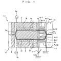
- FIG. 1 is a schematic view showing an optical modulator 11-1 to which an optical waveguide device 10 according to a first embodiment of the present invention is applied.
- the optical modulator 11-1 shown in FIG. 1 is formed by connecting RF signal generators 6a and 6b and a biasing power supply 7, which are hereinafter described, to the optical waveguide device 10 having a characteristic configuration according to the present invention.
- the optical waveguide device 10 shown in FIG. 1 includes a substrate 1Z, and further includes an optical waveguide 2, signal electrodes 3a and 3b, a bias electrode 4 and a ground electrode 5 formed on the substrate 1Z.
- the substrate 1Z has a configuration wherein LiNbO 3 (lithium niobate) which is a material having an electro-optical effect is cut in vertical to the Z-axis of crystal orientation or a Z-cut direction.
- a Mach-Zehnder type waveguide 2 including a light incoming side Y-branch waveguide 2a, linear waveguides 2b and 2c and a light outgoing side Y-branch waveguide 2d is formed on the substrate 1Z.
- the optical waveguide 2 described above is formed on the substrate 1Z and functions as an interference type optical waveguide wherein the lights propagating along the plurality of optical waveguides (that is, two linear waveguides 2b and 2c) extending in parallel to each other interfere with each other at the Y-branch waveguide 2d.
- the signal electrodes 3a and 3b are formed on the linear waveguides 2b and 2c, respectively.
- the signal electrode 3a functions as a first signal electrode formed on the linear waveguide 2b as one of the two optical waveguides which extend in parallel to each other and form the interference type optical waveguide 2
- the signal electrode 3b functions as a second signal electrode formed on the linear waveguide 2c as the other optical waveguide. Consequently, also in the optical waveguide device 10 shown in FIG. 1, similarly as in the optical waveguide device 100 shown in FIG. 3, a dual electrode structure wherein the signal electrodes 3a and 3b are formed on the linear waveguides 2b and 2c is formed.
- the signal electrodes 3a and 3b are connected to RF (Radio Frequency) signal generators 6a and 6b which generate RF signals having phases opposite to each other and apply the RF signals from the RF signal generators 6a and 6b as signals for optical modulation, respectively.
- RF Radio Frequency
- the bias electrode 4 is provided to bias signal components to be applied to the signal electrodes 3a and 3b, and includes a first bias electrode 4a and a second bias electrode 4b.
- the first and second bias electrodes 4a and 4b have a comb-like electrode structure so that bias voltages applied to the linear waveguides 2b and 2c which form the Mach-Zehnder type optical waveguide 2 are different from each other.
- V 0, the ground potential
- the first potential supplying electrode section 4a-1 of the bias electrode section 4a is configured as a trunk of the comb-like formation described above, and the first waveguide electrode section 4a-2 and two second potential difference producing electrode sections 4a-31 and 4a-32 are configured as branches of the comb-like formation described above.
- the second potential supplying electrode section 4b-1 of the bias electrode section 4b is configured as a trunk of the comb-like formation described above, and the second waveguide electrode section 4b-2 and two first potential difference producing electrode sections 4b-31 and 4b-32 are configured as branches of the comb-like formation described above.
- first and second bias electrodes 4a and 4b complement the potentials thereof each other, the voltages having an equal absolute value but having the opposite signs to each other are applied to the linear waveguides 2b and 2c.
- the ground electrode 5 is formed only within a range within which an electric field originating from the voltages applied to the signal electrodes 3a and 3b mainly has an influence, but is not formed within another range within which an electric field originating from the voltage applied to the bias electrode 4 described above has an influence.
- the optical waveguide device As described above, with the optical waveguide device according to the first embodiment of the present invention, also where the dual electrode structure wherein the signal electrodes 3a and 3b are formed on the linear waveguides 2b and 2c is used, voltages having an equal absolute value but having the opposite signs to each other can be applied from the bias electrode 4 while only the single biasing power supply 7 is utilized. Therefore, the optical waveguide device is advantageous in that the number of power supplies to be prepared can be decreased, and that it can contribute to reduction of the operation cost of an optical communication system.
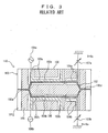
- FIG. 2 is a schematic view showing an optical modulator 11-2 to which an optical waveguide device according to a second embodiment of the present invention is applied.
- the optical modulator 11-2 shown in FIG. 2 is different, when compared with that in the first embodiment described hereinabove, in that separate power supplies 7a and 7b are connected to the first and second potential supplying electrode sections 4a-1 and 4b-1, respectively, such that the first and second potentials to be applied to the first and second potential supplying electrode sections 4a-1 and 4b-1 are potentials having an equal absolute value but having the opposite signs to each other.
- the optical waveguide device 10 in the present embodiment has a configuration similar to that of the first embodiment described above. It is to be noted that, in FIG. 2, basically like elements to those of FIG. 1 are denoted by like reference characters.
- the absolute value of the voltage values generated by the power supplies 7a and 7b is equal to one half that of the power supply 7 in the first embodiment.
- first and second bias electrodes 4a and 4b complement the potentials thereof each other, the voltages having an equal absolute value but having the opposite signs to each other are applied to the linear waveguides 2b and 2c.
- the optical waveguide device according to the second embodiment of the present invention, similarly as in the case of the dual electrode structure wherein the signal electrodes 3a and 3b are formed on the linear waveguides 2b and 2c, also where an optical modulator is formed without reducing the number of power supplies, while the voltage values to be generated are reduced to one half those of the conventional power supplies for the bias electrode, the voltages equal to those of the conventional optical waveguide devices are supplied as the bias voltage values . Therefore, the optical waveguide device is advantageous that it can contribute to reduction of the operation cost of an optical communication system.
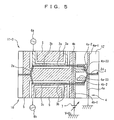
- FIG. 5 is a schematic view showing an optical modulator to which an optical waveguide device according to the third embodiment of the present invention is applied.
- the optical modulator 11-3 shown in FIG. 5 is different, when compared with the optical modulators of the first and second embodiments, in that (not two but) one first potential difference producing electrode section 4b-33 is provided in the proximity of the first waveguide electrode 4a-2, and a single second potential difference producing electrode section 4a-33 is provided also in the proximity of the second waveguide electrode 4b-2.
- FIG. 5 basically like elements to those of FIG. 1 and 2 are denoted by like reference characters.
- the optical waveguide device is advantageous in that it can contribute to reduction of the operation cost of an optical communication system.
- a Mach-Zehnder type optical waveguide is applied as the interference type optical waveguide
- any other known interference type optical waveguide can be applied as the interference type optical waveguide.
- the bias electrode 4 is formed as a bias electrode for biasing the signal components to be applied to the signal electrodes 3a and 3b on the two linear waveguides 2b and 2c which form a Mach-Zehnder type optical modulator, the present invention is not limited to the specific configuration but can be applied similarly also where the bias electrode 4 is formed a bias electrode for biasing signal components to be applied to signal electrodes for three or more parallel optical waveguides.
- the bias electrode includes not only first and second potential supplying electrode portions similar to those in the embodiments described above but also comb branch-like waveguide electrode portions formed on the three or more parallel optical waveguides at the stage next to the signal electrodes for alternately receiving potentials from the first and second potential supplying electrode portions in order of the parallel arrangement of the three or more optical waveguides, and at least comb branch-like potential difference producing electrode portions formed in such a manner as to sandwich the waveguide electrodes therebetween to which the potential from one of the potential supplying electrode portions is supplied for supplying the potential from the other one of the potential supplying electrode portions.
- the bias electrode can apply voltages having an equal absolute value but having the opposite signs to each other to adjacent ones of the three or more parallel waveguides since the potentials to be supplied to adjacent ones of the optical waveguides complement each other.
- the present invention can be applied also to an optical waveguide device which at least includes a substrate cut in the Z-axis direction and having an electro-optical effect, such an interference type optical waveguide as described above, and a lumped-constant type electrode for applying voltages for the electro-optical effect described above to lights propagating along optical waveguides which form the interference type optical waveguide if the lumped-constant type optical electrode is configured similarly to any of the bias electrodes in the embodiments described above.
- optical waveguide device according to the present invention can be produced in accordance with the embodiments described above.
Landscapes
- Physics & Mathematics (AREA)
- Nonlinear Science (AREA)
- General Physics & Mathematics (AREA)
- Optics & Photonics (AREA)
- Optical Modulation, Optical Deflection, Nonlinear Optics, Optical Demodulation, Optical Logic Elements (AREA)
- Optical Integrated Circuits (AREA)
Abstract
Description
Claims (8)
- An optical waveguide device, characterized in that it comprises:a substrate (1Z) cut in a Z-axis direction and having an electro-optical effect;an interference type optical waveguide (2) formed on said substrate (1Z) for causing lights which propagate along a plurality of parallel optical waveguides (2b, 2c) to interfere with each other; anda lumped-constant type electrode (4) for applying voltages for the electro-optical effect to the respective lights propagating along said optical waveguides (2b, 2c) which form said interference type optical waveguide (2);said lumped-constant type electrode (4) complementing potentials to be supplied to adjacent ones of said plurality of parallel optical waveguides (2b, 2c) each other such that voltages having an equal absolute value but having the opposite signs are applied to the adjacent optical waveguides.
- An optical waveguide device, characterized in that it comprises:a substrate (1Z) cut in a Z-axis direction and having an electro-optical effect;an interference type optical waveguide(2) formed on said substrate (1Z) for causing lights which propagate along a plurality of parallel optical waveguides (2b, 2c) to interfere with each other;a plurality of signal electrodes (3a, 3b) formed respectively on said optical waveguides (2b, 2c) which form said interference type optical waveguide (2); anda bias electrode (4) for biasing signal components to be applied to the respective signal electrodes (3a, 3b); and thatsaid bias electrode (4) complements potentials to be supplied to adjacent ones of said plurality of parallel optical waveguides (2b, 2c) each other such that voltages having an equal absolute value but having the opposite signs are applied to the adjacent optical waveguides.
- The optical waveguide device as set forth in claim 2, characterized in that said bias electrode (4) includes:a first potential supplying electrode section (4a-1) to which a first potential is applied;a second potential supplying electrode section (4b-1) to which a second potential different from the first potential is applied;a plurality of waveguide electrode sections (4a-2, 4b-2) formed respectively on said optical waveguides (2b, 2c) at a next stage to said signal electrodes (3a, 3b) for receiving the potentials alternately from said first and second potential supplying electrode sections (4a-1, 4b-1) in order of the parallel arrangement of said plurality of optical waveguides (2b, 2c); andat least one potential difference producing electrode section (4a-33, 4b-33) disposed in the proximity of that one of said waveguide electrode sections (4a-2, 4b-2), which supplies the potential from one of said first and second potential supplying electrode sections (4a-1, 4b-1), for supplying the potential supplied from the other of said first and second potential supplying electrode sections (4a-1, 4b-1).
- The optical waveguide device as set forth in claim 3, characterized in that one of the first and second potentials supplied from said first and second potential supplying electrode sections (4a-1, 4b-1) is the ground potential.
- The optical waveguide device as set forth in claim 3, characterized in that the first and second potentials supplied from said first and second potential supplying electrode sections (4a-1, 4b-1) are potentials having an equal absolute value but having the opposite signs.
- An optical waveguide device, characterized in that it comprises:a substrate (1Z) cut in a Z-axis direction and having an electro-optical effect;an interference type optical waveguide (2) formed on said substrate (1Z) for causing lights which propagate along two parallel optical waveguides (2b, 2c) to interfere with each other;a first signal electrode (3a) formed on one of said two parallel optical waveguides (2b, 2c) which form said interference type optical waveguide;a second signal electrode (3b) formed on the other of said two parallel optical waveguides (2b, 2c) which form said interference type optical waveguide;a first bias electrode (4a) for biasing a signal component to be applied to said first signal electrode (3a); anda second bias electrode (4b) for biasing a signal component to be applied to said second signal electrode (3b); said first and second bias electrodes (4a, 4b) complementing the potentials thereof each other such that voltages having an equal absolute value but having the opposite signs are applied to said two parallel optical waveguides (2b, 2c).
- The optical waveguide device as set forth in claim 6, characterized in that said bias electrode (4a, 4b) includes:a first potential supplying electrode (4a-1) section to which a first potential is applied;a second potential supplying electrode (4b-1) section to which a second potential different from the first potential is applied;a first waveguide electrode section (4a-2) formed on the one optical waveguide (2b) at a next stage to said first signal electrode (3a) for receiving the potential supplied from said first potential supplying electrode section (4a-1);a second waveguide electrode section (4b-2) formed on the other optical waveguide (2c) at a next stage to said second signal electrode (3b) for receiving the potential supplied from said second potential supplying electrode section (4b-1);a first potential difference producing electrode sections (4b-31, 4b-32) formed in such a manner as to sandwich said first waveguide electrode (4a-2) section therebetween for supplying the potential from said second potential supplying electrode section (4b-1); anda second potential difference producing electrode sections (4a-31, 4a-32) formed in such a manner as to sandwich said second waveguide electrode section (4b-2) therebetween for supplying the potential from said first potential supplying electrode section (4a-1).
- The optical waveguide device as set forth in any one of claims 1, 2, and 6, characterized in that said interference type optical waveguide (2) is a Mach-Zehnder type optical waveguide.
Applications Claiming Priority (2)
| Application Number | Priority Date | Filing Date | Title |
|---|---|---|---|
| JP2002031483 | 2002-02-07 | ||
| JP2002031483A JP3806043B2 (en) | 2002-02-07 | 2002-02-07 | Optical waveguide device |
Publications (3)
| Publication Number | Publication Date |
|---|---|
| EP1336893A2 true EP1336893A2 (en) | 2003-08-20 |
| EP1336893A3 EP1336893A3 (en) | 2005-03-30 |
| EP1336893B1 EP1336893B1 (en) | 2012-10-10 |
Family
ID=27621378
Family Applications (1)
| Application Number | Title | Priority Date | Filing Date |
|---|---|---|---|
| EP02026801A Expired - Lifetime EP1336893B1 (en) | 2002-02-07 | 2002-11-28 | Optical waveguide device |
Country Status (3)
| Country | Link |
|---|---|
| US (1) | US7239764B2 (en) |
| EP (1) | EP1336893B1 (en) |
| JP (1) | JP3806043B2 (en) |
Cited By (1)
| Publication number | Priority date | Publication date | Assignee | Title |
|---|---|---|---|---|
| US8467033B2 (en) | 2008-02-25 | 2013-06-18 | Carl Zeiss Smt Gmbh | Method for operating an illumination system of a microlithographic projection exposure apparatus |
Families Citing this family (15)
| Publication number | Priority date | Publication date | Assignee | Title |
|---|---|---|---|---|
| JP2006221111A (en) * | 2005-02-14 | 2006-08-24 | Nippon Telegr & Teleph Corp <Ntt> | Mach-Zehnder type optical element and driving method thereof |
| JP2008039859A (en) | 2006-08-01 | 2008-02-21 | Fujitsu Ltd | Light modulator |
| JP5056040B2 (en) * | 2007-02-08 | 2012-10-24 | 富士通株式会社 | Light modulator |
| JP5050003B2 (en) * | 2008-11-19 | 2012-10-17 | アンリツ株式会社 | Light modulator |
| JP5487774B2 (en) * | 2009-07-27 | 2014-05-07 | 富士通オプティカルコンポーネンツ株式会社 | Optical device and optical transmitter |
| JP5421935B2 (en) * | 2011-01-14 | 2014-02-19 | アンリツ株式会社 | Light modulator |
| CN103728693B (en) * | 2013-12-26 | 2016-01-06 | 华中师范大学 | A kind of array of photoswitch chip based on digital optical phase conjugation principle |
| JP6394244B2 (en) * | 2014-09-30 | 2018-09-26 | 住友大阪セメント株式会社 | Light control element |
| JP2016142755A (en) * | 2015-01-29 | 2016-08-08 | 富士通オプティカルコンポーネンツ株式会社 | Light modulator |
| JP6350563B2 (en) | 2016-02-29 | 2018-07-04 | 住友大阪セメント株式会社 | Optical modulator and optical transmitter using the optical modulator |
| JP6249031B2 (en) | 2016-03-18 | 2017-12-20 | 住友大阪セメント株式会社 | Optical modulator and optical transmitter using the optical modulator |
| JP2017181676A (en) * | 2016-03-29 | 2017-10-05 | 住友大阪セメント株式会社 | Optical waveguide element |
| JP6288140B2 (en) | 2016-03-29 | 2018-03-07 | 住友大阪セメント株式会社 | Optical waveguide device |
| JP6227069B1 (en) | 2016-07-27 | 2017-11-08 | 富士通オプティカルコンポーネンツ株式会社 | Light modulator |
| WO2024054243A2 (en) * | 2022-01-24 | 2024-03-14 | Arizona Board Of Regents On Behalf Of The University Of Arizona | Optical waveguide components possessing high nonlinear efficiency and adaptive-profile poling process to fabricate the same |
Family Cites Families (12)
| Publication number | Priority date | Publication date | Assignee | Title |
|---|---|---|---|---|
| US4273411A (en) * | 1980-01-24 | 1981-06-16 | Bell Telephone Laboratories, Incorporated | Optical wavelength filter |
| JPS6214627A (en) | 1985-07-12 | 1987-01-23 | Oki Electric Ind Co Ltd | Waveguide type optical switch |
| US5015053A (en) * | 1989-04-25 | 1991-05-14 | Massachusetts Institute Of Technology | Reduction of modulator non-linearities with independent bias angle control |
| US5032805A (en) * | 1989-10-23 | 1991-07-16 | The United States Of America As Represented By The Secretary Of The Army | RF phase shifter |
| JPH04332878A (en) | 1991-05-07 | 1992-11-19 | Toyota Central Res & Dev Lab Inc | Electromagnetic field intensity measuring device |
| CA2083219C (en) * | 1991-11-19 | 1999-01-05 | Hiroshi Nishimoto | Optical transmitter having optical modulator |
| US5278923A (en) * | 1992-09-02 | 1994-01-11 | Harmonic Lightwaves, Inc. | Cascaded optical modulation system with high linearity |
| US5434700A (en) * | 1993-12-16 | 1995-07-18 | Bell Communications Research, Inc. | All-optical wavelength converter |
| GB2344658B (en) | 1996-04-03 | 2000-08-23 | Gen Instrument Corp | Optical modulator for CATV systems |
| JPH11231358A (en) | 1998-02-19 | 1999-08-27 | Nec Corp | Optical circuit and manufacturing method thereof |
| JP2000275590A (en) | 1999-03-29 | 2000-10-06 | Sumitomo Osaka Cement Co Ltd | Waveguide type optical modulator |
| US6222965B1 (en) * | 1999-07-08 | 2001-04-24 | Agere Systems Opto Electronics Guardian Inc. | Bias control system for electrooptic devices |
-
2002
- 2002-02-07 JP JP2002031483A patent/JP3806043B2/en not_active Expired - Lifetime
- 2002-11-19 US US10/298,560 patent/US7239764B2/en not_active Expired - Lifetime
- 2002-11-28 EP EP02026801A patent/EP1336893B1/en not_active Expired - Lifetime
Cited By (5)
| Publication number | Priority date | Publication date | Assignee | Title |
|---|---|---|---|---|
| US8467033B2 (en) | 2008-02-25 | 2013-06-18 | Carl Zeiss Smt Gmbh | Method for operating an illumination system of a microlithographic projection exposure apparatus |
| US9217931B2 (en) | 2008-02-25 | 2015-12-22 | Carl Zeiss Smt Gmbh | Method for operating an illumination system of a microlithographic projection exposure apparatus |
| US9341957B2 (en) | 2008-02-25 | 2016-05-17 | Carl Zeiss Smt Gmbh | Method for operating an illumination system of a microlithographic projection exposure apparatus |
| US9703206B2 (en) | 2008-02-25 | 2017-07-11 | Carl Zeiss Smt Gmbh | Method for operating an illumination system of a microlithographic projection exposure apparatus |
| US10222704B2 (en) | 2008-02-25 | 2019-03-05 | Carl Zeiss Smt Gmbh | Method for operating an illumination system of a microlithographic projection exposure apparatus |
Also Published As
| Publication number | Publication date |
|---|---|
| EP1336893B1 (en) | 2012-10-10 |
| JP3806043B2 (en) | 2006-08-09 |
| EP1336893A3 (en) | 2005-03-30 |
| US7239764B2 (en) | 2007-07-03 |
| US20030147576A1 (en) | 2003-08-07 |
| JP2003233042A (en) | 2003-08-22 |
Similar Documents
| Publication | Publication Date | Title |
|---|---|---|
| EP1336893B1 (en) | Optical waveguide device | |
| EP4028829B1 (en) | Integrated electro-optic frequency comb generator | |
| JP2603437B2 (en) | Periodic domain inversion electro-optic modulator | |
| US7286727B2 (en) | Optical communication device and optical device | |
| KR0136969B1 (en) | Optical modulator for producing a controllable chirp | |
| US7058241B2 (en) | Optical modulator | |
| CN113359367B (en) | Optical device including optical modulator and optical transceiver | |
| US9568751B2 (en) | Optical control device | |
| EP2116889B1 (en) | Optical phase modulator | |
| US6580840B1 (en) | High efficiency electro-optic modulator with equalized frequency response | |
| EP2015130A1 (en) | Optical waveguide device based on a delay interferometer for transmitting return-to-zero pulses | |
| JP2008116865A (en) | Nested modulator | |
| JP5007629B2 (en) | Optical waveguide device | |
| US20090290206A1 (en) | Optical waveguide device | |
| CN101238405A (en) | Optical modulator | |
| US6643051B1 (en) | Method and system for generating return-to-zero signals | |
| US6567203B1 (en) | Tri-electrode traveling wave optical modulators and methods | |
| JP4751601B2 (en) | Light modulator | |
| JP4587762B2 (en) | Light modulation element module | |
| JP2010152306A (en) | Optical modulator | |
| JP2007333753A (en) | Electro-optic SSB optical modulator and optical frequency shifter | |
| US6738174B1 (en) | Dual-electrode traveling wave optical modulators and methods | |
| US7095543B1 (en) | Dual-electrode traveling wave optical phase shifters and methods | |
| JP2002365596A (en) | Optical transmitter with modulator comprising a plurality of modulation elements | |
| JP5622293B2 (en) | Nested modulator |
Legal Events
| Date | Code | Title | Description |
|---|---|---|---|
| PUAI | Public reference made under article 153(3) epc to a published international application that has entered the european phase |
Free format text: ORIGINAL CODE: 0009012 |
|
| AK | Designated contracting states |
Designated state(s): AT BE BG CH CY CZ DE DK EE ES FI FR GB GR IE IT LI LU MC NL PT SE SK TR |
|
| AX | Request for extension of the european patent |
Extension state: AL LT LV MK RO SI |
|
| PUAL | Search report despatched |
Free format text: ORIGINAL CODE: 0009013 |
|
| AK | Designated contracting states |
Kind code of ref document: A3 Designated state(s): AT BE BG CH CY CZ DE DK EE ES FI FR GB GR IE IT LI LU MC NL PT SE SK TR |
|
| AX | Request for extension of the european patent |
Extension state: AL LT LV MK RO SI |
|
| 17P | Request for examination filed |
Effective date: 20050412 |
|
| AKX | Designation fees paid |
Designated state(s): DE GB |
|
| 17Q | First examination report despatched |
Effective date: 20080115 |
|
| GRAP | Despatch of communication of intention to grant a patent |
Free format text: ORIGINAL CODE: EPIDOSNIGR1 |
|
| GRAS | Grant fee paid |
Free format text: ORIGINAL CODE: EPIDOSNIGR3 |
|
| GRAA | (expected) grant |
Free format text: ORIGINAL CODE: 0009210 |
|
| AK | Designated contracting states |
Kind code of ref document: B1 Designated state(s): DE GB |
|
| REG | Reference to a national code |
Ref country code: GB Ref legal event code: FG4D |
|
| REG | Reference to a national code |
Ref country code: DE Ref legal event code: R096 Ref document number: 60243830 Country of ref document: DE Effective date: 20121206 |
|
| PLBE | No opposition filed within time limit |
Free format text: ORIGINAL CODE: 0009261 |
|
| STAA | Information on the status of an ep patent application or granted ep patent |
Free format text: STATUS: NO OPPOSITION FILED WITHIN TIME LIMIT |
|
| 26N | No opposition filed |
Effective date: 20130711 |
|
| REG | Reference to a national code |
Ref country code: DE Ref legal event code: R097 Ref document number: 60243830 Country of ref document: DE Effective date: 20130711 |
|
| PGFP | Annual fee paid to national office [announced via postgrant information from national office to epo] |
Ref country code: GB Payment date: 20151125 Year of fee payment: 14 Ref country code: DE Payment date: 20151125 Year of fee payment: 14 |
|
| REG | Reference to a national code |
Ref country code: DE Ref legal event code: R119 Ref document number: 60243830 Country of ref document: DE |
|
| GBPC | Gb: european patent ceased through non-payment of renewal fee |
Effective date: 20161128 |
|
| PG25 | Lapsed in a contracting state [announced via postgrant information from national office to epo] |
Ref country code: GB Free format text: LAPSE BECAUSE OF NON-PAYMENT OF DUE FEES Effective date: 20161128 Ref country code: DE Free format text: LAPSE BECAUSE OF NON-PAYMENT OF DUE FEES Effective date: 20170601 |