EP1335643A2 - Method for manufacturing double-sided circuit board - Google Patents
Method for manufacturing double-sided circuit board Download PDFInfo
- Publication number
- EP1335643A2 EP1335643A2 EP03002532A EP03002532A EP1335643A2 EP 1335643 A2 EP1335643 A2 EP 1335643A2 EP 03002532 A EP03002532 A EP 03002532A EP 03002532 A EP03002532 A EP 03002532A EP 1335643 A2 EP1335643 A2 EP 1335643A2
- Authority
- EP
- European Patent Office
- Prior art keywords
- electrically insulating
- electric conductor
- insulating layer
- layer
- film
- Prior art date
- Legal status (The legal status is an assumption and is not a legal conclusion. Google has not performed a legal analysis and makes no representation as to the accuracy of the status listed.)
- Withdrawn
Links
Images


Classifications
-
- H—ELECTRICITY
- H05—ELECTRIC TECHNIQUES NOT OTHERWISE PROVIDED FOR
- H05K—PRINTED CIRCUITS; CASINGS OR CONSTRUCTIONAL DETAILS OF ELECTRIC APPARATUS; MANUFACTURE OF ASSEMBLAGES OF ELECTRICAL COMPONENTS
- H05K1/00—Printed circuits
- H05K1/02—Details
- H05K1/0213—Electrical arrangements not otherwise provided for
- H05K1/0263—High current adaptations, e.g. printed high current conductors or using auxiliary non-printed means; Fine and coarse circuit patterns on one circuit board
- H05K1/0265—High current adaptations, e.g. printed high current conductors or using auxiliary non-printed means; Fine and coarse circuit patterns on one circuit board characterized by the lay-out of or details of the printed conductors, e.g. reinforced conductors, redundant conductors, conductors having different cross-sections
-
- H—ELECTRICITY
- H05—ELECTRIC TECHNIQUES NOT OTHERWISE PROVIDED FOR
- H05K—PRINTED CIRCUITS; CASINGS OR CONSTRUCTIONAL DETAILS OF ELECTRIC APPARATUS; MANUFACTURE OF ASSEMBLAGES OF ELECTRICAL COMPONENTS
- H05K3/00—Apparatus or processes for manufacturing printed circuits
- H05K3/46—Manufacturing multilayer circuits
-
- H—ELECTRICITY
- H05—ELECTRIC TECHNIQUES NOT OTHERWISE PROVIDED FOR
- H05K—PRINTED CIRCUITS; CASINGS OR CONSTRUCTIONAL DETAILS OF ELECTRIC APPARATUS; MANUFACTURE OF ASSEMBLAGES OF ELECTRICAL COMPONENTS
- H05K3/00—Apparatus or processes for manufacturing printed circuits
- H05K3/40—Forming printed elements for providing electric connections to or between printed circuits
- H05K3/42—Plated through-holes or plated via connections
- H05K3/421—Blind plated via connections
-
- H—ELECTRICITY
- H05—ELECTRIC TECHNIQUES NOT OTHERWISE PROVIDED FOR
- H05K—PRINTED CIRCUITS; CASINGS OR CONSTRUCTIONAL DETAILS OF ELECTRIC APPARATUS; MANUFACTURE OF ASSEMBLAGES OF ELECTRICAL COMPONENTS
- H05K3/00—Apparatus or processes for manufacturing printed circuits
- H05K3/40—Forming printed elements for providing electric connections to or between printed circuits
- H05K3/42—Plated through-holes or plated via connections
- H05K3/425—Plated through-holes or plated via connections characterised by the sequence of steps for plating the through-holes or via connections in relation to the conductive pattern
- H05K3/426—Plated through-holes or plated via connections characterised by the sequence of steps for plating the through-holes or via connections in relation to the conductive pattern initial plating of through-holes in substrates without metal
-
- H—ELECTRICITY
- H05—ELECTRIC TECHNIQUES NOT OTHERWISE PROVIDED FOR
- H05K—PRINTED CIRCUITS; CASINGS OR CONSTRUCTIONAL DETAILS OF ELECTRIC APPARATUS; MANUFACTURE OF ASSEMBLAGES OF ELECTRICAL COMPONENTS
- H05K3/00—Apparatus or processes for manufacturing printed circuits
- H05K3/40—Forming printed elements for providing electric connections to or between printed circuits
- H05K3/42—Plated through-holes or plated via connections
- H05K3/425—Plated through-holes or plated via connections characterised by the sequence of steps for plating the through-holes or via connections in relation to the conductive pattern
- H05K3/427—Plated through-holes or plated via connections characterised by the sequence of steps for plating the through-holes or via connections in relation to the conductive pattern initial plating of through-holes in metal-clad substrates
-
- H—ELECTRICITY
- H05—ELECTRIC TECHNIQUES NOT OTHERWISE PROVIDED FOR
- H05K—PRINTED CIRCUITS; CASINGS OR CONSTRUCTIONAL DETAILS OF ELECTRIC APPARATUS; MANUFACTURE OF ASSEMBLAGES OF ELECTRICAL COMPONENTS
- H05K2201/00—Indexing scheme relating to printed circuits covered by H05K1/00
- H05K2201/03—Conductive materials
- H05K2201/0332—Structure of the conductor
- H05K2201/0335—Layered conductors or foils
- H05K2201/0352—Differences between the conductors of different layers of a multilayer
-
- H—ELECTRICITY
- H05—ELECTRIC TECHNIQUES NOT OTHERWISE PROVIDED FOR
- H05K—PRINTED CIRCUITS; CASINGS OR CONSTRUCTIONAL DETAILS OF ELECTRIC APPARATUS; MANUFACTURE OF ASSEMBLAGES OF ELECTRICAL COMPONENTS
- H05K2201/00—Indexing scheme relating to printed circuits covered by H05K1/00
- H05K2201/03—Conductive materials
- H05K2201/0332—Structure of the conductor
- H05K2201/0335—Layered conductors or foils
- H05K2201/0355—Metal foils
-
- H—ELECTRICITY
- H05—ELECTRIC TECHNIQUES NOT OTHERWISE PROVIDED FOR
- H05K—PRINTED CIRCUITS; CASINGS OR CONSTRUCTIONAL DETAILS OF ELECTRIC APPARATUS; MANUFACTURE OF ASSEMBLAGES OF ELECTRICAL COMPONENTS
- H05K2201/00—Indexing scheme relating to printed circuits covered by H05K1/00
- H05K2201/03—Conductive materials
- H05K2201/0332—Structure of the conductor
- H05K2201/0388—Other aspects of conductors
- H05K2201/0394—Conductor crossing over a hole in the substrate or a gap between two separate substrate parts
-
- H—ELECTRICITY
- H05—ELECTRIC TECHNIQUES NOT OTHERWISE PROVIDED FOR
- H05K—PRINTED CIRCUITS; CASINGS OR CONSTRUCTIONAL DETAILS OF ELECTRIC APPARATUS; MANUFACTURE OF ASSEMBLAGES OF ELECTRICAL COMPONENTS
- H05K2201/00—Indexing scheme relating to printed circuits covered by H05K1/00
- H05K2201/09—Shape and layout
- H05K2201/09209—Shape and layout details of conductors
- H05K2201/095—Conductive through-holes or vias
- H05K2201/09509—Blind vias, i.e. vias having one side closed
-
- H—ELECTRICITY
- H05—ELECTRIC TECHNIQUES NOT OTHERWISE PROVIDED FOR
- H05K—PRINTED CIRCUITS; CASINGS OR CONSTRUCTIONAL DETAILS OF ELECTRIC APPARATUS; MANUFACTURE OF ASSEMBLAGES OF ELECTRICAL COMPONENTS
- H05K2201/00—Indexing scheme relating to printed circuits covered by H05K1/00
- H05K2201/09—Shape and layout
- H05K2201/09209—Shape and layout details of conductors
- H05K2201/09654—Shape and layout details of conductors covering at least two types of conductors provided for in H05K2201/09218 - H05K2201/095
- H05K2201/09736—Varying thickness of a single conductor; Conductors in the same plane having different thicknesses
-
- H—ELECTRICITY
- H05—ELECTRIC TECHNIQUES NOT OTHERWISE PROVIDED FOR
- H05K—PRINTED CIRCUITS; CASINGS OR CONSTRUCTIONAL DETAILS OF ELECTRIC APPARATUS; MANUFACTURE OF ASSEMBLAGES OF ELECTRICAL COMPONENTS
- H05K2203/00—Indexing scheme relating to apparatus or processes for manufacturing printed circuits covered by H05K3/00
- H05K2203/05—Patterning and lithography; Masks; Details of resist
- H05K2203/0562—Details of resist
- H05K2203/0574—Stacked resist layers used for different processes
-
- H—ELECTRICITY
- H05—ELECTRIC TECHNIQUES NOT OTHERWISE PROVIDED FOR
- H05K—PRINTED CIRCUITS; CASINGS OR CONSTRUCTIONAL DETAILS OF ELECTRIC APPARATUS; MANUFACTURE OF ASSEMBLAGES OF ELECTRICAL COMPONENTS
- H05K2203/00—Indexing scheme relating to apparatus or processes for manufacturing printed circuits covered by H05K3/00
- H05K2203/05—Patterning and lithography; Masks; Details of resist
- H05K2203/0562—Details of resist
- H05K2203/0577—Double layer of resist having the same pattern
-
- H—ELECTRICITY
- H05—ELECTRIC TECHNIQUES NOT OTHERWISE PROVIDED FOR
- H05K—PRINTED CIRCUITS; CASINGS OR CONSTRUCTIONAL DETAILS OF ELECTRIC APPARATUS; MANUFACTURE OF ASSEMBLAGES OF ELECTRICAL COMPONENTS
- H05K2203/00—Indexing scheme relating to apparatus or processes for manufacturing printed circuits covered by H05K3/00
- H05K2203/13—Moulding and encapsulation; Deposition techniques; Protective layers
- H05K2203/1377—Protective layers
- H05K2203/1394—Covering open PTHs, e.g. by dry film resist or by metal disc
-
- H—ELECTRICITY
- H05—ELECTRIC TECHNIQUES NOT OTHERWISE PROVIDED FOR
- H05K—PRINTED CIRCUITS; CASINGS OR CONSTRUCTIONAL DETAILS OF ELECTRIC APPARATUS; MANUFACTURE OF ASSEMBLAGES OF ELECTRICAL COMPONENTS
- H05K3/00—Apparatus or processes for manufacturing printed circuits
- H05K3/02—Apparatus or processes for manufacturing printed circuits in which the conductive material is applied to the surface of the insulating support and is thereafter removed from such areas of the surface which are not intended for current conducting or shielding
- H05K3/06—Apparatus or processes for manufacturing printed circuits in which the conductive material is applied to the surface of the insulating support and is thereafter removed from such areas of the surface which are not intended for current conducting or shielding the conductive material being removed chemically or electrolytically, e.g. by photo-etch process
- H05K3/061—Etching masks
- H05K3/064—Photoresists
-
- H—ELECTRICITY
- H05—ELECTRIC TECHNIQUES NOT OTHERWISE PROVIDED FOR
- H05K—PRINTED CIRCUITS; CASINGS OR CONSTRUCTIONAL DETAILS OF ELECTRIC APPARATUS; MANUFACTURE OF ASSEMBLAGES OF ELECTRICAL COMPONENTS
- H05K3/00—Apparatus or processes for manufacturing printed circuits
- H05K3/10—Apparatus or processes for manufacturing printed circuits in which conductive material is applied to the insulating support in such a manner as to form the desired conductive pattern
- H05K3/108—Apparatus or processes for manufacturing printed circuits in which conductive material is applied to the insulating support in such a manner as to form the desired conductive pattern by semi-additive methods; masks therefor
-
- H—ELECTRICITY
- H05—ELECTRIC TECHNIQUES NOT OTHERWISE PROVIDED FOR
- H05K—PRINTED CIRCUITS; CASINGS OR CONSTRUCTIONAL DETAILS OF ELECTRIC APPARATUS; MANUFACTURE OF ASSEMBLAGES OF ELECTRICAL COMPONENTS
- H05K3/00—Apparatus or processes for manufacturing printed circuits
- H05K3/38—Improvement of the adhesion between the insulating substrate and the metal
- H05K3/388—Improvement of the adhesion between the insulating substrate and the metal by the use of a metallic or inorganic thin film adhesion layer
-
- Y—GENERAL TAGGING OF NEW TECHNOLOGICAL DEVELOPMENTS; GENERAL TAGGING OF CROSS-SECTIONAL TECHNOLOGIES SPANNING OVER SEVERAL SECTIONS OF THE IPC; TECHNICAL SUBJECTS COVERED BY FORMER USPC CROSS-REFERENCE ART COLLECTIONS [XRACs] AND DIGESTS
- Y10—TECHNICAL SUBJECTS COVERED BY FORMER USPC
- Y10T—TECHNICAL SUBJECTS COVERED BY FORMER US CLASSIFICATION
- Y10T29/00—Metal working
- Y10T29/49—Method of mechanical manufacture
- Y10T29/49002—Electrical device making
- Y10T29/49117—Conductor or circuit manufacturing
- Y10T29/49124—On flat or curved insulated base, e.g., printed circuit, etc.
- Y10T29/49128—Assembling formed circuit to base
-
- Y—GENERAL TAGGING OF NEW TECHNOLOGICAL DEVELOPMENTS; GENERAL TAGGING OF CROSS-SECTIONAL TECHNOLOGIES SPANNING OVER SEVERAL SECTIONS OF THE IPC; TECHNICAL SUBJECTS COVERED BY FORMER USPC CROSS-REFERENCE ART COLLECTIONS [XRACs] AND DIGESTS
- Y10—TECHNICAL SUBJECTS COVERED BY FORMER USPC
- Y10T—TECHNICAL SUBJECTS COVERED BY FORMER US CLASSIFICATION
- Y10T29/00—Metal working
- Y10T29/49—Method of mechanical manufacture
- Y10T29/49002—Electrical device making
- Y10T29/49117—Conductor or circuit manufacturing
- Y10T29/49124—On flat or curved insulated base, e.g., printed circuit, etc.
- Y10T29/49155—Manufacturing circuit on or in base
- Y10T29/49156—Manufacturing circuit on or in base with selective destruction of conductive paths
-
- Y—GENERAL TAGGING OF NEW TECHNOLOGICAL DEVELOPMENTS; GENERAL TAGGING OF CROSS-SECTIONAL TECHNOLOGIES SPANNING OVER SEVERAL SECTIONS OF THE IPC; TECHNICAL SUBJECTS COVERED BY FORMER USPC CROSS-REFERENCE ART COLLECTIONS [XRACs] AND DIGESTS
- Y10—TECHNICAL SUBJECTS COVERED BY FORMER USPC
- Y10T—TECHNICAL SUBJECTS COVERED BY FORMER US CLASSIFICATION
- Y10T428/00—Stock material or miscellaneous articles
- Y10T428/24—Structurally defined web or sheet [e.g., overall dimension, etc.]
- Y10T428/24802—Discontinuous or differential coating, impregnation or bond [e.g., artwork, printing, retouched photograph, etc.]
- Y10T428/24917—Discontinuous or differential coating, impregnation or bond [e.g., artwork, printing, retouched photograph, etc.] including metal layer
Definitions
- the present invention relates to a method for manufacturing a double-sided circuit board having electric conductor wiring formed on opposite surfaces of an electrically insulating layer, and particularly to a manufacturing method suitable for manufacturing a flexible circuit board.
- a double-sided circuit board according to the related art is generally manufactured by a method shown in Figs. 6A to 6G. That is, as shown in Fig. 6A, there is used a printed board material 6 which has an electrically insulating layer 61 such as a layer of polyimide, and electric conductor layers 62 such as layers of copper foil formed on opposite surfaces of the electrically insulating layer 61. As shown in Fig. 6B, conduction holes 63 are formed in the material 6 by drilling using a laser, a mold, or the like, by chemical dissolution or by a method using both drilling and chemical dissolution in combination. Then, as shown in Fig.
- an electrically conductive thin-film layer 64 is formed on wall surfaces of the conduction holes 63 by a method such as chemical treatment, vapor deposition or sputtering.
- an electric conductor layer 65 such as a layer of copper is formed by electroplating on all the front and rear surfaces of the board material 6 inclusive of all the surface of the thin-film layer 64.
- the electric conductor layer 65 is covered with photosensitive films 66. Then, as shown in Fig.
- an additive method in which an electric conductor wiring is formed on an electrically insulating board by electroplating is known as another method than the subtractive method.
- stress generated inevitably in the electrically insulating board material due to carrying tension in a continuous carrying (sheeting) process is too large to be neglected because the electrically insulating board material is shaped like a flexible film.
- dimensional stability is lowered or the flexible circuit board is apt to be curled.
- flexing characteristic such as bending characteristic of the flexible circuit board deteriorates because the electric conductor wiring is made of an electrolytically deposited metal.
- the additive method is not suitable for the method of manufacturing a double-sided circuit board requiring sufficient flexing characteristic.
- the invention is developed for solving the problems inherent in the related art, and an object of the invention is to provide a method for manufacturing a double-sided circuit board, which can meet the requirement of high-density fine wiring and by which a double-sided circuit board having high dimensional stability, hardly curled and adapted for a flex purpose can be obtained when the method is used for manufacturing a flexible circuit board.
- the invention provides a method of manufacturing a double-sided circuit board from a board material constituted by a first electric conductor layer and a first electrically insulating layer formed on one surface of the first electric conductor layer, including: the first step of making conduction holes in the board material so that the conduction holes penetrate only the first electrically insulating layer or both the first electrically insulating layer and the first electric conductor layer from predetermined portions of the first electrically insulating layer; the second step of forming an electrically conductive thin-film layer both on a surface of the first electrically insulating layer and on wall surfaces of the conduction holes; the third step of forming a second electrically insulating layer on at least one predetermined portion of the electrically conductive thin-film layer; the fourth step of forming a first electric conductor wiring by plating on a portion of the electrically conductive thin-film layer where the second electrically insulating layer is not formed; the fifth step of covering the first electric conductor wiring with a chemical-resistant film; the first step of making conduction
- the first electric conductor wiring can meet the requirement of high-density fine wiring because the first electric conductor wiring is formed by plating. That is, the first electric conductor wiring can be formed uniformly without being influenced by the wiring width or the gap width, and the difference between the wiring width in the surface and the wiring width in the bottom can be reduced extremely.
- the second electric conductor wiring per se can hardly meet the requirement of high-density fine wiring because the second electric conductor wiring is formed by the so-called subtractive method, that is, by chemically dissolving the predetermined portion of the other surface of the first electric conductor layer in chemicals to remove the predetermined portion.
- the double-sided circuit board manufactured can meet the requirement of high-density fine wiring as a whole because wiring can be drawn from the second electric conductor wiring to the first electric conductor wiring through the conduction holes.
- the manufacturing method according to the invention is used for manufacturing a flexible circuit board, influence of carrying tension in a continuous carrying (sheeting) process can be reduced greatly because the first electric conductor layer has been already formed on the first electrically insulating layer (flexible film-like electrically insulating layer in this case) in the fourth step of forming the first electric conductor wiring by plating.
- a double-sided circuit board having high dimensional stability and hardly curled can be obtained. That is, because the electrical conductor layer is generally more elastic than the electrically insulating layer, stress generated in the board material is dispersed or relaxed by the presence of the first electric conductor layer so that the influence of carrying tension can be reduced greatly.
- the second electrically insulating layer is formed on portions requiring flexing characteristic such as bending characteristic so that the first electric conductor wiring can be prevented from being formed on the portions by plating (in addition, portions of the other surface of the first electric conductor layer where the first electric conductor wiring is not formed are chemically dissolved as occasion demands).
- flexing characteristic such as bending characteristic
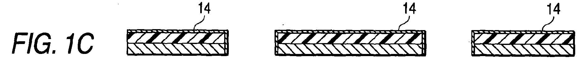
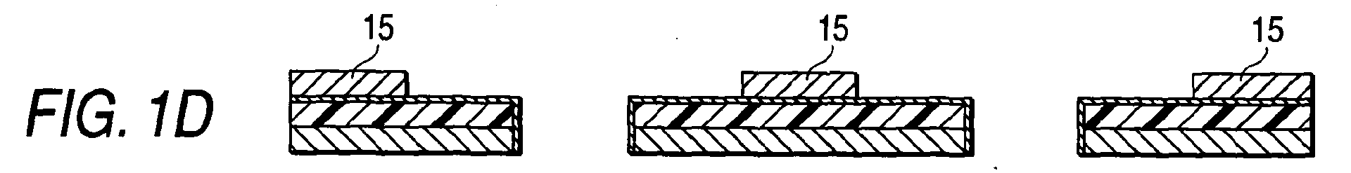
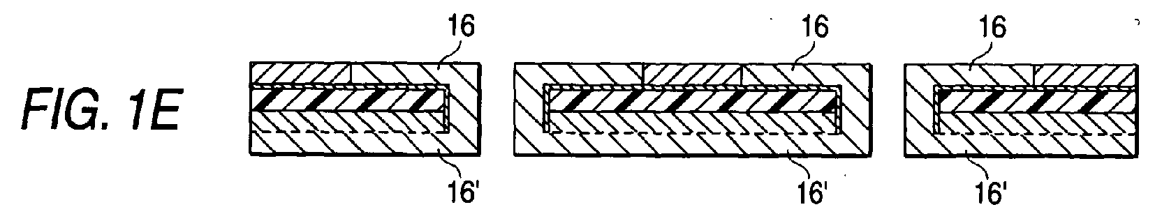
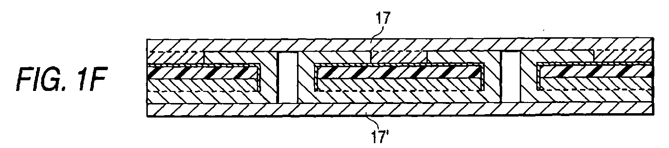
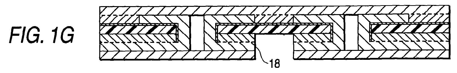
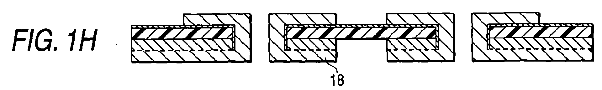
- Figs. 1A to 1I are views for explaining a method of manufacturing a double-sided circuit board according to a first embodiment of the invention.
- a board material 1 having a first electric conductor layer 11, and a first electrically insulating layer 12 formed on one surface of the first electric conductor layer 11 is used in the manufacturing method according to this embodiment.
- a layer of a metal or metal foil capable of being treated with chemicals, such as copper foil, copper alloy, stainless steel, or nickel is preferably used as the first electric conductor layer 11.
- the thickness of the first electric conductor layer 11 is generally selected to be in a range of from 1 ⁇ m to 100 ⁇ m, preferably in a range of from 3 ⁇ m to 30 ⁇ m.
- the first electrically insulating layer 12 is preferably used as the first electrically insulating layer 12.
- the thickness of the first electrically insulating layer 12 is generally selected to be in a range of from 3 ⁇ m to 200 ⁇ m, preferably in a range of from 5 ⁇ m to 100 ⁇ m.
- conduction holes 13 are formed in the board material 1 so that the conduction holes 13 penetrate both the first electrically insulating layer 12 and the first electric conductor layer 11 from predetermined portions of the first electrically insulating layer 12.
- the method for forming the conduction holes 13 there may be used a known method such as drilling using a laser, a mold or the like, dissolution using chemicals, or use of a photosensitive resin.
- the diameter of each of the conduction holes 13 is generally selected to be in a range of from 10 ⁇ m to 500 ⁇ m, preferably in a range of from 30 ⁇ m to 300 ⁇ m.
- an electrically conductive thin-film layer 14 is formed both on the surface of the first electrically insulating layer 12 and on wall surfaces of the conduction holes 13.
- Ni, Cr, Cu, Ni/Cr alloy, Cu/Ni alloy, Ti or an alloy of these metals is preferably used as the material of the electrically conductive thin-film layer 14.
- Cr-based metal such as Cr or Ni/Cr alloy is preferably used as the material of the electrically conductive thin-film layer 14.
- the thickness of the electrically conductive thin-film layer 14 is generally selected to be in a range of from 3 ⁇ to 3000 ⁇ , preferably in range of from 5 ⁇ to 2000 ⁇ .
- the electrically conductive thin-film layer 14 is not limited to a single layer but may be provided as a laminate of a plurality of layers in accordance with necessity.
- a second electrically insulating layer 15 is formed on predetermined portions of the electrically conductive thin-film layer 14.
- a material having resistance to electrolytic plating solution is used as the material of the second electrically insulating layer 15.
- the thickness of the second electrically insulating layer 15 is preferably selected to be larger than the plating thickness of a first electric conductor wiring 16 which will be described later.
- the second electrically insulating layer 15 is formed as a 15 ⁇ m-thick layer.
- a photosensitive electrically insulating material may be used as an example of the material of the second electrically insulating layer 15 so that portions of the electrically insulating material corresponding to the pattern of the electric conductor wiring are exposed and developed and then non-developed portions of the electrically insulating material are dissolved.
- the first electric conductor wiring 16 is formed by electroplating on the portions of the electrically conductive thin-film layer 14 where the second electrically insulating layer 15 is not formed.
- an electric conductor layer 16' is formed by electroplating on the other surface of the first electric conductor layer 11 where the electrically conductive thin-film layer 14 is not formed.
- the electroplating is performed by immersing the board material 1 in an electrolytic plating solution of copper sulfate and applying electricity to the electrolytic plating solution.
- the first electric conductor wiring 16 is covered with a film 17, for example, having chemical resistance to acid such as ferric chloride or cupric chloride.
- a film 17 for example, having chemical resistance to acid such as ferric chloride or cupric chloride.
- a photosensitive electrically insulating material is used as the material of the film 17.
- the film 17 having such chemical resistance is formed.
- a film 17' similar to the film 17 is formed on the electric conductor layer 16'.
- the film 17' is however different from the film 17 in that only portions of the film 17' corresponding to a pattern of a second electric conductor wiring 18 which will be described later are exposed and developed so as to have chemical resistance whereas the whole surface of the film 17 is exposed and developed.
- the film 17' is different from the second electrically insulating layer 15 in that the film 17' functions as a protective film when the second electric conductor wiring 18 which will be described later is formed by a subtractive method.
- the thickness of the film 17' is as small as possible (e,g., 15 ⁇ m or smaller) .
- the film 17' is formed by use of a liquid resist.
- a second electric conductor wiring 18 is formed by chemically dissolving predetermined portions of the other surface of the first electric conductor layer 11 (inclusive of predetermined portions of the film 17' and the electric conductor layer 16' in this embodiment) in chemicals. That is, the second electric conductor wiring 18 is formed by a subtractive method.
- acid such as ferric chloride or cupric chloride
- dissolution of the electric conductor layer in this embodiment is used.
- the films 17 and 17' and the second electrically insulating layer 15 are removed.
- the films 17 and 17' and the second electrically insulating layer 15 can be separated and removed by alkaline chemicals.
- the electrically conductive thin-film layer 14 remaining on the first electrically insulating layer 12 is removed.
- a double-sided circuit board 10 having the first electric conductor wiring 16 and the second electric conductor wiring 18 is completed.
- the electrically conductive thin-film layer 14 can be separated and removed by acidic chemicals.
- the first and second electric conductor wirings 1.6 and 18 by electroplating are not formed on the predetermined portion 19 of the double-sided circuit board 10 manufactured by the method according to this embodiment but the predetermined portion 19 is constituted by only the first electrically insulating layer 12.
- the first electrically insulating layer 12 is made of a flexible film-like material, sufficient flexing characteristic can be obtained in this portion 19.
- Figs. 2A to 2I are views for explaining a method of manufacturing a double-sided circuit board according to a second embodiment of the invention.
- a board material 2 having a first electric conductor layer 21, and a first electrically insulating layer 22 formed on one surface of the first electric conductor layer 21 is used in the manufacturing method according to this embodiment, like the first embodiment.
- the preferred materials for forming the first electric conductor layer 21 and the first electrically insulating layer 22 and the preferred thicknesses of the materials are the same as those in the first embodiment.
- conduction holes 23 are formed in the board material 2 so that the conduction holes 23 penetrate both the first electrically insulating layer 22 and the first electric conductor layer 21 from predetermined portions of the first electrically insulating layer 22.
- the preferred method for forming the conduction holes 23 and the preferred diameter of each of the conduction holes 23 are the same as those in the first embodiment.
- an electrically conductive thin-film layer 24 is formed both on the surface of the first electrically insulating layer 22 and on wall surfaces of the conduction holes 23.
- the preferred material of the electrically conductive thin-film layer 24 and the preferred thickness of the electrically conductive thin-film layer 24 are the same as those in the first embodiment.
- a second electrically insulating layer 25 is formed on predetermined portions of the electrically conductive thin-film layer 24.
- an electrically insulating layer 25' is also formed on a predetermined portion of the other surface of the first electric conductor layer 21.
- the preferred materials of the second electrically insulating layer 25 and the electrically insulating layer 25' and the preferred thicknesses thereof are the same as those of the second electrically insulating layer 15 in the first embodiment.
- a first electric conductor wiring 26 is formed by electroplating on the portions of the electrically conductive thin-film layer 24 where the second electrically insulating layer 25 is not formed.
- an electric conductor layer 26' is also formed by electroplating on portions where the electrically insulating layer 25' is not formed, among portions of the other surface of the first electric conductor layer 21 where the electrically conductive thin-film layer 24 is not formed.
- the electroplating is performed by. immersing the board material 2 in an electrolytic plating solution of copper sulfate and applying electricity to the electrolytic plating solution in the same manner as in the first embodiment.
- the first electric conductor wiring 26 is covered with a film 27, for example, having chemical resistance to acid such as ferric chloride or cupric chloride.
- a film 27' similar to the film 27 is also formed on the electric conductor layer 26' in the same manner as in the first embodiment.
- the preferred materials of the films 27 and 27' and the preferred thicknesses of the films 27 and 27' are the same as those of the films 17 and 17' in the first embodiment.
- a second electric conductor wiring 28 is formed by chemically dissolving predetermined portions of the other surface of the first electric conductor layer 21 (inclusive of predetermined portions of the film 27' and the electric conductor layer 26' in this embodiment) in chemicals.
- the dissolution method is the same as in the first embodiment.
- the films 27 and 27', the second electrically insulating layer 25 and the electrically insulating layer 25' are removed.
- the method for removing these films and layers is the same as in the first embodiment.
- the electrically conductive thin-film layer 24 remaining on the first electrically insulating layer 22 is removed.
- a double-sided circuit board 20 having the first electric conductor wiring 26 and the second electric conductor wiring 28 is completed.
- the method for removing the electrically conductive thin-film film 24 is the same as in the first embodiment.
- the first electric conductor wiring 26 by electroplating is not formed on a predetermined portion 29 of the double-sided circuit board 20 manufactured by the method according to this embodiment but the predetermined portion 29 is constituted by the first electrically insulating layer 22 and the first electric conductor layer 21.
- the first electrically insulating layer 22 is made of a flexible film-like material and the first electric conductor layer 21 is made of a rolled sheet of copper foil or the like, sufficient flexing characteristic can be obtained in this portion 29.
- Figs. 3A to 3I are views for explaining a method of manufacturing a double-sided circuit board according to a third embodiment of the invention.
- a board material 3 having a first electric conductor layer 31, and a first electrically insulating layer 32 formed on one surface of the first electric conductor layer 31 is used in the manufacturing method according to this embodiment, like the first embodiment.
- the preferred materials for forming the first electric conductor layer 31 and the first electrically insulating layer 32 and the preferred thicknesses of the first electric conductor layer 31 and the first electrically insulating layer 32 are the same as those in the first embodiment.
- conduction holes 33 are formed in the board material 3 so that the conduction holes 33 penetrate both the first electrically insulating layer 32 and the first electric conductor layer 31 from predetermined portions of the first electrically insulating layer 32.
- the preferred method for forming the conduction holes 33 and the preferred diameter of each of the conduction holes 33 are the same as those in the first embodiment.
- an electrically conductive thin-film layer 34 is formed both on the surface of the first electrically insulating layer 32 and on wall surfaces of the conduction holes 33.
- the preferred material of the electrically conductive thin-film layer 34 and the preferred thickness thereof are the same as those in the first embodiment.
- a second electrically insulating layer 35 is formed on predetermined portions of the electrically conductive thin-film layer 34.
- an electrically insulating layer 35' is also formed on the whole of the other surface of the first electric conductor layer 31.
- the preferred materials of the second electrically insulating layer 35 and the electrically insulating layer 35' and the preferred thicknesses thereof are the same as those of the second electrically insulating layer 15 in the first embodiment.
- a first electric conductor wiring 36 is formed by electroplating on the portions of the electrically conductive thin-film layer 34 where the second electrically insulating layer 35 is not formed.
- an electric conductor layer is not formed by electroplating on the other surface of the first electric conductor layer 31 because the electrically insulating layer 35' is. formed on the whole of the other surface of the first electric conductor layer 31.
- the electroplating is performed by immersing the board material 3 in an electrolytic plating solution of copper sulfate in the same manner as in the first embodiment.
- the first electric conductor wiring 36 is covered with a. film 37, for example, having chemical resistance to acid such as ferric chloride or cupric chloride.
- a film 37' similar to the film 37 is formed on the electrically insulating layer 35' in the same manner as in the first embodiment.
- the preferred materials of the films 37 and 37' and the preferred thicknesses thereof are the same as those of the films 17 and 17' in the first embodiment.
- a second electric conductor wiring 38 is formed by chemically dissolving a predetermined portion of the other surface of the first electric conductor layer 31 (inclusive of predetermined portions of the film 37' and the electrically insulating layer 35' in this embodiment) in chemicals.
- the dissolution method is the same as in the first embodiment.
- the films 37 and 37', the second electrically insulating layer 35 and the electrically insulating layer 35' are removed.
- the method for removing these films and layers is the same as in the first embodiment.
- the electrically conductive thin-film layer 34 remaining on the first electrically insulating layer 32 is removed.
- a double-sided circuit board 30 having the first electric conductor wiring 36 and the second electric conductor wiring 38 is completed.
- the method for removing the electrically conductive thin-film layer 34 is the same as in the first embodiment.
- Figs. 4A to 4I are views for explaining a method of manufacturing a double-sided circuit board according to a fourth embodiment of the invention.
- a board material 4 having a first electric conductor layer 41, and a first electrically insulating layer 42 formed on one surface of the first electric conductor layer 41 is used in the manufacturing method according to this embodiment, like the first embodiment.
- the preferred materials for forming the first electric conductor layer 41 and the first electrically insulating layer 42 and the preferred thicknesses thereof are the same as those in the first embodiment.
- conduction holes 43 are formed in the board material 4 so that the conduction holes penetrate only the first electrically insulating layer 42 from predetermined portions of the first electrically insulating layer 42.
- the preferred method for forming the conduction holes 43 and the preferred diameter of each of the conduction holes 43 are the same as those in the first embodiment.
- an electrically conductive thin-film layer 44 is formed on bottoms of the conduction holes 43, that is, on exposed surfaces of the first electric conductor layer 41 as well as the electrically conductive thin-film layer 44 is formed both on the surface of the first electrically insulating layer 42 and on wall surfaces of the conduction holes 43.
- the preferred material of the electrically conductive thin-film layer 44 and the preferred thickness thereof are the same as those in the first embodiment.
- a second electrically insulating layer 45 is formed on predetermined portions of the electrically conductive thin-film layer 44.
- an electrically insulating layer 45' is also formed on the whole of the other surface of the first electric conductor layer 41.
- the preferred materials of the second electrically insulating layer 45 and the electrically insulating layer 45' and the preferred thicknesses thereof are the same as those of the second electrically insulating layer 15 in the first embodiment.
- a first electric conductor wiring 46 is formed by electroplating on the portions of the electrically conductive thin-film layer 44 where the second electrically insulating layer 45 is not formed.
- the electric conductor layer by electroplating is not formed on the other surface of the first electric conductor layer 41 because the electrically insulating layer 45' is formed on the whole of the other surface of the first electric conductor layer 41.
- the electroplating is performed by immersing the board material 4 in an electrolytic plating solution of copper sulfate in the same manner as in the first embodiment.
- the first electric conductor wiring 46 is covered with a film 47, for example, having chemical resistance to acid such as ferric chloride or cupric chloride.
- a film 47' similar to the film 47 is formed on the electrically insulating layer 45' in the same manner as in the first embodiment.
- the preferred materials of the films 47 and 47' and the preferred thicknesses thereof are the same as those of the films 17 and 17' in the first embodiment.
- a second electric conductor wiring 48 is formed by chemically dissolving predetermined portions of the other surface of the first electric conductor layer 41 (inclusive of predetermined portions of the film 47' and the electrically insulating layer 45' in this embodiment) in chemicals.
- the dissolution method is the same as in the first embodiment.
- the films 47 and 47', the second electrically insulating layer 45 and the electrically insulating layer 45' are removed.
- the method for removing these films and layers is the same as in the first embodiment.
- the electrically conductive thin-film layer 44 remaining on the first electrically insulating layer 42 is removed.
- a double-sided circuit board 40 having the first electric conductor wiring 46 and the second electric conductor wiring 48 is completed.
- the method for removing the electrically conductive thin-film layer 44 is the same as in the first embodiment.
- Figs. 5A to 5I are views for explaining a method of manufacturing a double-sided circuit board according to a fifth embodiment of the invention.
- a board material 5 having a first electric conductor layer 51, and a first electrically insulating layer 52 formed on one surface of the first electric conductor layer 51 is used in the manufacturing method according to this embodiment, like the first embodiment.
- the preferred materials for forming the first electric conductor layer 51 and the first electrically insulating layer 52 and the preferred thicknesses thereof are the same as those in the first embodiment.
- conduction holes 53 are formed in the board material 5 so that the conduction holes 53 penetrate only the first electrically insulating layer 52 from predetermined portions of the first electrically insulating layer 52.
- the preferred method for forming the conduction holes 53 and the preferred diameter of each of the conduction holes 53 are the same as those in the first embodiment.
- an electrically conductive thin-film layer 54 is formed on the surface of the first electrically insulating layer 52, wall surfaces of the conduction holes 53, and bottoms of the conduction holes 53.
- the preferred material of the electrically conductive thin-film layer 54 and the preferred thickness thereof are the same as those in the first embodiment.
- a second electrically insulating layer 55 is formed on a predetermined portion of the electrically conductive thin-film layer 54.
- an electrically insulating layer 55' is also formed on the whole of the other surface of the first electric conductor layer 51.
- the preferred materials of the second electrically insulating layer 55 and the electrically insulating layer 55' and the preferred thicknesses thereof are the same as those of the second electrically insulating layer 15 in the first embodiment.
- a first electric conductor wiring 56 is formed by electroplating on the portion of the electrically conductive thin-film layer 54 where the second electrically insulating layer 55 is not formed.
- an electric conductor layer by electroplating is not formed on the other surface of the first electric conductor layer 51 because the electrically insulating layer 55' is formed on the whole of the other surface of the first electric conductor layer 51.
- the electroplating is performed by immersing the board material 5 in an electrolytic plating solution of copper sulfate and applying electricity to the electrolytic plating solution in the same manner as in the first embodiment.
- the first electric conductor wiring 56 is covered with a film 57, for example, having chemical resistance to acid such as ferric chloride or cupric chloride.
- a film 57' similar to the film 57 is formed on the electrically insulating layer 55' in the same manner as in the first embodiment.
- the preferred materials of the films 57 and 57' and the preferred thicknesses thereof are the same as those of the films 17 and 17' in the first embodiment.
- a second electric conductor wiring 58 is formed by chemically dissolving predetermined portions of the other surface of the first electric conductor layer 51 (inclusive of predetermined portions of the film 57' and the electrically insulating layer 55' in this embodiment) in chemicals.
- the dissolution method is the same as in the first embodiment.
- a predetermine portion of the first electric conductor wiring 56 is also dissolved so that a predetermined pattern of the first electric conductor wiring 56 is formed.
- the films 57 and 57', the second electrically insulating layer 55 and the electrically insulating layer 55' are removed.
- the method for removing these films and layers is the same as in the first embodiment.
- the electrically conductive thin-film layer 54 remaining on the first electrically insulating layer 52 is removed.
- a double-sided circuit board 50 having the first electric conductor wiring 56 and the second electric conductor wiring 58 is completed.
- the method for removing the electrically conductive thin-film layer 54 is the same as in the first embodiment.
- an electrically insulating layer (cover layer) may be formed on the first electric conductor wiring and the second electric conductor wiring in accordance with necessity, and surface treatment such as gold plating may be further applied to the electrically insulating layer in accordance with necessity.
- a double-sided circuit board was manufactured by the manufacturing method according to the first embodiment shown in Figs. 1A to 1I.
- a board material 1 there was used a copper-clad laminate (e.g., ESPANEX made by Nippon Steel Chemical Co., Ltd. or NEOFLEX made by Mitsui Chemicals Inc.) in which a first electrically insulating layer 12 made of a polyimide resin with a thickness of 25 ⁇ m was formed directly on one surface of a first electric conductor layer 11 made of copper foil with a thickness of 12 ⁇ m.
- conduction holes 13 each having a diameter of 75 ⁇ m were formed by a YAG laser.
- an electrically conductive thin-film layer 14 made of an Ni/Cr alloy with a thickness of 500 ⁇ was formed by sputtering.
- a photosensitive electrically insulating film e.g., SPG152 made by Asahi Kasei Corp.
- the second electrically insulating layer 15 was developed in an alkaline solution.
- the board material 1 was immersed in an electrolytic plating solution of copper sulfate and plated at the rate of 2.5A/dm 2 for about 18 minutes to thereby form a first electric conductor wiring 16 made of a copper plating with a thickness of 8 ⁇ m. Further, an electric conductor layer 16' made of a copper plating with a thickness of 8 ⁇ m was formed on the whole of the other surface of the first electric conductor layer 11. Thus, a copper layer having a total thickness of 20 ⁇ m was formed as a combination of the first electric conductor layer 11 and the electric conductor layer 16'.
- a photosensitive electrically insulating film (e.g., SFG102 made by Asahi Kasei Corp.) having a thickness of 10 ⁇ m was laminated on the resulting laminate.
- the 20 ⁇ m-thick copper layer was dissolved in ferric chloride to thereby form a second electric conductor wiring 18.
- the films 17 and 17', the second electrically insulating layer 15 and the electrically conductive thin-film layer 14 were removed.
- a double-sided circuit board 10 was obtained.
- the first electric conductor wiring 16 was formed uniformly and the difference between the wiring width in the surface and the wiring width in the bottom was reduced extremely in the double-sided circuit board 10 manufactured according to this example.
- the double-sided circuit board 10 was produced as a board having high dimensional stability, hardly curled and having sufficient flexing characteristic.
- a double-sided circuit board was manufactured by the manufacturing method according to the second embodiment shown in Figs. 2A to 2I.
- a board material 2 there was used a copper-clad laminate (e.g., ESPANEX made by Nippon Steel Chemical Co., Ltd. or NEOFLEX made by Mitsui Chemicals Inc.) in which a first electrically insulating layer 22 made of a polyimide resin with a thickness of 12 ⁇ m was formed directly on one surface of a first electric conductor layer 21 made of copper foil with a thickness of 12 ⁇ m.
- conduction holes 23 each having a diameter of 100 ⁇ m were formed by a YAG laser.
- an electrically conductive thin-film layer 24 made of an Ni/Cu alloy with a thickness of 300 ⁇ was formed by sputtering.
- a photosensitive electrically insulating film e.g., SPG152 made by Asahi Kasei Corp.
- the second electrically insulating layer 25 and the electrically insulating layer 25' were irradiated with ultraviolet light while predetermined positions were covered with glass masks capable of shielding the light, the second electrically insulating layer 25 and the electrically insulating layer 25' were developed in an alkaline solution.
- the board material 2 was immersed in an electrolytic plating solution of copper sulfate and plated at the rate of 2.5A/dm 2 for about 20 minutes to thereby form a first electric conductor wiring 26 made of a copper plating with a thickness of 10 ⁇ m. Further, an electric conductor layer 26' made of a copper plating with a thickness of 10 ⁇ m was formed on portions which were on the other surface of the first electric conductor layer 21 and on which the electrically insulating layer 25' was not formed. Thus, a copper layer having a total thickness of 22 ⁇ m was formed as a combination of the first electric conductor layer 21 and the electric conductor layer 26'.
- a photosensitive electrically insulating film (e.g., RY3206 made by Hitachi Chemical Co., Ltd.) having a thickness of 6 ⁇ m was laminated on the resulting laminate.
- the film 27' was exposed and developed in accordance with a desired wiring pattern, the 22 ⁇ m-thick copper layer was dissolved in ferric chloride to thereby form a second electric conductor wiring 28.
- the films 27 and 27', the second electrically insulating layer 25, the electrically insulating layer 25' and the electrically conductive thin-film layer 24 were removed.
- a double-sided circuit board 20 was obtained.
- the first electric conductor wiring 26 was formed uniformly and the difference between the wiring width in the surface and the wiring width in the bottom was reduced extremely in the double-sided circuit board 20 manufactured according to this example.
- the double-sided circuit board 20 was produced as aboard having high dimensional stability, hardly curled and having sufficient flexing characteristic.
- a double-sided circuit board was manufactured by the manufacturing method according to the third embodiment shown in Figs. 3A to 3I.
- a board material 3 there was used a copper-clad laminate (e.g., ESPANEX made by Nippon Steel Chemical Co., Ltd. or NEOFLEX made by Mitsui Chemicals Inc.) in which a first electrically insulating layer 32 made of a polyimide resin with a thickness of 12 ⁇ m was formed directly on one surface of a first electric conductor layer 31 made of copper foil with a thickness of 18 ⁇ m. Then, conduction holes 33 each having a diameter of 150 ⁇ m were formed by punching.
- ESPANEX made by Nippon Steel Chemical Co., Ltd. or NEOFLEX made by Mitsui Chemicals Inc.
- an electrically conductive thin-film layer 34 made of Cr with a thickness of 400 ⁇ was formed by sputtering.
- a photosensitive electrically insulating film e.g., SPG252 made by Asahi Kasei Corp.
- the second electrically insulating layer 35 and the electrically insulating layer 35' were irradiated with ultraviolet light while predetermined positions were covered with glass masks capable of shielding the light, the second electrically insulating layer 35 and the electrically insulating layer 35' were developed in an alkaline solution.
- the board material 3 was immersed in an electrolytic plating solution of copper sulfate and plated at the rate of 2.5A/dm 2 for about 36 minutes to thereby form a first electric conductor wiring 36 made of a copper plating with a thickness of 18 ⁇ m.
- a photosensitive electrically insulating film e.g., RY3206 made by Hitachi Chemical Co. Ltd.
- the 18 ⁇ m-thick first electric conductor layer 31 was dissolved in ferric chloride to thereby form a second electric conductor wiring 38.
- the films 37 and 37', the second electrically insulating layer 35, the electrically insulating layer 35' and the electrically conductive thin-film layer 34 were removed.
- a double-sided circuit board 30 was obtained. It was confirmed that the first electric conductor wiring 36 was formed uniformly and the difference between the wiring width in the surface and the wiring width in the bottom was reduced extremely in the double-sided circuit board 30 manufactured according to this example.
- the double-sided circuit board 30 was produced as a board having high dimensional stability, hardly curled and having sufficient flexing characteristic.
- a double-sided circuit board was manufactured by the manufacturing method according to the fourth embodiment shown in Figs. 4A to 4I.
- a board material 4 there was used a copper-clad laminate (e.g., ESPANEX made by Nippon Steel Chemical Co., Ltd. or NEOFLEX made by Mitsui Chemicals Inc.) in which a first electrically insulating layer 42 made of a polyimide resin with a thickness of 12 ⁇ m was formed directly on one surface of a first electric conductor layer 41 made of copper foil with a thickness of 18 ⁇ m. Then, conduction holes 43 each having a diameter of 80 ⁇ m were formed by chemicals.
- ESPANEX made by Nippon Steel Chemical Co., Ltd. or NEOFLEX made by Mitsui Chemicals Inc.
- conduction holes 43 each having a diameter of 80 ⁇ m were formed by chemicals.
- SPG252 made by Asahi Kasei Corp.
- the second electrically insulating layer 45 and the electrically insulating layer 45' were irradiated with ultraviolet light while predetermined positions were covered with glass masks capable of shielding the light, the second electrically insulating layer 45 and the electrically insulating layer 45' were developed in an alkaline solution. Then, the board material 4 was immersed in an electrolytic plating solution of copper sulfate and plated at the rate of 2.5A/dm 2 for about 18 minutes to thereby form a first electric conductor wiring 46 made of a copper plating with a thickness of 8 ⁇ m.
- a photosensitive electrically insulating film for example, RY3206 made by Hitachi Chemical Co., Ltd.
- RY3206 made by Hitachi Chemical Co., Ltd.
- the 18 ⁇ m-thick first electric conductor layer 41 was dissolved in ferric chloride to thereby form a second electric conductor wiring 48.
- the films 47 and 47', the second electrically insulating layer 45, the electrically insulating layer 45' and the electrically conductive thin-film layer 44 were removed.
- a double-sided circuit board 40 was obtained.
- the first electric conductor wiring 46 was formed uniformly and the difference between the wiring width in the surface and the wiring width in the bottom was reduced extremely in the double-sided circuit board 40 manufactured according to this example.
- the double-sided circuit board 40 was produced as a board having high dimensional stability, hardly curled and having sufficient flexing characteristic.
- a double-sided circuit board was manufactured by the manufacturing method according to the fifth embodiment shown in Figs. 5A to 5I.
- a copper-clad laminate in which a first electrically insulating layer 52 made of a photosensitive polyimide resin with a thickness of 12 ⁇ m was formed directly on one surface of a first electric conductor layer 51 made of copper foil with a thickness of 18 ⁇ m.
- conduction holes 53 each having a diameter of 80 ⁇ m were formed by chemicals.
- an electrically conductive thin-film layer 54 made of an Ni/Cr alloy with a thickness of 400 ⁇ was formed by sputtering.
- a photosensitive electrically insulating film (e.g., SPG252 made by Asahi Kasei Corp.) having a thickness of 25 ⁇ m was laminated on the resulting laminate.
- the second electrically insulating layer 55 and the electrically insulating layer 55' were irradiated with ultraviolet light while predetermined positions were covered with glass masks capable of shielding the light, the second electrically insulating layer 55 and the electrically insulating layer 55' were developed in an alkaline solution.
- the board material 5 was immersed in an electrolytic plating solution of copper sulfate and plated at the rate of 2.5A/dm 2 for about 36 minutes to thereby form a first electric conductor wiring 56 made of a copper plating with a thickness of 18 ⁇ m.
- a photosensitive electrically insulating film e.g., RY3206 made by Hitachi Chemical Co., Ltd.
- the 18 ⁇ m-thick first electric conductor layer 51 was dissolved in ferric chloride to thereby form a second electric conductor wiring 58.
- the double-sided circuit board 50 was obtained. It was confirmed that the first electric conductor wiring 56 was formed uniformly and the difference between the wiring width in the surface and the wiring width in the bottom was reduced extremely in the double-sided circuit board 50 manufactured according to this example. In addition, the double-sided circuit board 50 was produced as a board having high dimensional stability, hardly curled and having sufficient flexing characteristic.
- a semiconductor device or the like can be mounted on the first electric conductor:wiring side to meet the requirement of high-density fine wiring. That is, the first electric conductor wiring can be formed uniformly without being influenced by the wiring width or the gap width, and the difference between the wiring width in the surface and the wiring width in the bottom can be reduced extremely.
- the manufacturing method according to the invention is used for manufacturing a flexible circuit board, the influence of carrying tension in a continuous carrying (sheeting) process can be reduced greatly because the first electric conductor layer has been already formed on the first electrically insulating layer in the step of forming the first electric conductor wiring by electroplating. As a result, a double-sided circuit board having high dimensional stability and hardly curled can be obtained.
- a second electrically insulating layer is formed on portions requiring flexing characteristic such as bending characteristic so that so that the first electric conductor wiring can be prevented from being formed on the portions by plating (in addition, portions of the other surface of the first electric conductor layer where the first electric conductor wiring is not formed are dissolved chemically as occasion demands). Accordingly, sufficient flexing characteristic can be obtained.
Landscapes
- Engineering & Computer Science (AREA)
- Microelectronics & Electronic Packaging (AREA)
- Manufacturing & Machinery (AREA)
- Manufacturing Of Printed Wiring (AREA)
- Printing Elements For Providing Electric Connections Between Printed Circuits (AREA)
- Laminated Bodies (AREA)
- Manufacturing Of Printed Circuit Boards (AREA)
Abstract
Description
Claims (5)
- A method of manufacturing a double-sided circuit board from a board material constituted by a first electric conductor layer and a first electrically insulating layer formed on one surface of the first electric conductor layer, comprising:a first step of making conduction holes in said board material so that said conduction holes penetrate only said first electrically insulating layer or both said first electrically insulating layer and said first electric conductor layer from predetermined portions of said first electrically insulating layer;a second step of forming an electrically.conductive thin-film layer both on a surface of said first electrically insulating layer and on wall surfaces of said conduction holes;a third step of forming a second electrically insulating layer on at least one predetermined portion of said electrically conductive thin-film layer;a fourth step of forming a first electric conductor wiring by plating on a portion of said electrically conductive thin-film layer where said second electrically insulating layer is not formed;a fifth step of covering said first electric conductor wiring with a chemical-resistant film;a sixth step of forming a second electric conductor wiring by chemically dissolving at least one predetermined portion of another surface of said first electric conductor layer in chemicals; anda seventh step of removing said second electrically insulating layer and said chemical-resistant film.
- A method of manufacturing a double-sided circuit board according to claim 1, wherein second electrically insulating layers are formed on at least one predetermined portion of said electrically conductive thin-film layer and on at least one predetermined portion of said another surface of the first electric conductor layer in the third step.
- A method of manufacturing a double-sided circuit board according to claim 2, wherein the second electrically insulating layers are formed on the whole of said another surface of the first electric conductor layer in the third step.
- A method of manufacturing a double-sided circuit board according to claim 1, wherein said conduction holes penetrate only said first electrically insulating layer.
- A method of manufacturing a double-sided circuit board according to claim 1, wherein a predetermined portion of said first conductor wiring is chemically dissolved in chemicals so that a predetermined pattern of said first conductor wiring is formed in said sixth step.
Applications Claiming Priority (2)
| Application Number | Priority Date | Filing Date | Title |
|---|---|---|---|
| JP2002029643A JP2003234572A (en) | 2002-02-06 | 2002-02-06 | Method for manufacturing double-sided wiring board |
| JP2002029643 | 2002-02-06 |
Publications (2)
| Publication Number | Publication Date |
|---|---|
| EP1335643A2 true EP1335643A2 (en) | 2003-08-13 |
| EP1335643A3 EP1335643A3 (en) | 2005-01-19 |
Family
ID=27606493
Family Applications (1)
| Application Number | Title | Priority Date | Filing Date |
|---|---|---|---|
| EP03002532A Withdrawn EP1335643A3 (en) | 2002-02-06 | 2003-02-05 | Method for manufacturing double-sided circuit board |
Country Status (6)
| Country | Link |
|---|---|
| US (1) | US6889432B2 (en) |
| EP (1) | EP1335643A3 (en) |
| JP (1) | JP2003234572A (en) |
| KR (1) | KR100590369B1 (en) |
| CN (1) | CN1221158C (en) |
| TW (1) | TW556462B (en) |
Cited By (2)
| Publication number | Priority date | Publication date | Assignee | Title |
|---|---|---|---|---|
| EP1513382A3 (en) * | 2003-09-08 | 2007-05-23 | FCM Co., Ltd. | Conductive sheet having conductive layer with improved adhesion and product including the same |
| CN114069161A (en) * | 2017-02-07 | 2022-02-18 | 捷温有限责任公司 | Film capable of conducting electricity |
Families Citing this family (10)
| Publication number | Priority date | Publication date | Assignee | Title |
|---|---|---|---|---|
| JP4330486B2 (en) | 2004-05-07 | 2009-09-16 | 日東電工株式会社 | Method for manufacturing double-sided printed wiring board |
| JP4150401B2 (en) * | 2006-02-28 | 2008-09-17 | 日東電工株式会社 | Double-sided wiring board |
| US7992287B2 (en) * | 2007-11-06 | 2011-08-09 | Xerox Corporation | System for thinning a transducer with improved thickness uniformity |
| KR101411717B1 (en) * | 2008-07-16 | 2014-06-26 | 삼성전자주식회사 | Fabrication method for printed circuit board |
| US8413324B2 (en) * | 2009-06-09 | 2013-04-09 | Ibiden Co., Ltd. | Method of manufacturing double-sided circuit board |
| US9930789B2 (en) | 2010-04-12 | 2018-03-27 | Seagate Technology Llc | Flexible printed circuit cable with multi-layer interconnection and method of forming the same |
| CN102355794B (en) * | 2011-09-16 | 2016-04-06 | 珠海市超赢电子科技有限公司 | A kind of Double-layer flexible circuit board |
| US20150305166A1 (en) | 2014-04-22 | 2015-10-22 | Carestream Health, Inc. | Laser patterning of dual sided transparent conductive films |
| TWI578416B (en) * | 2015-09-18 | 2017-04-11 | 旭德科技股份有限公司 | Package carrier board and manufacturing method thereof |
| CN115568085B (en) * | 2021-07-01 | 2024-08-09 | 深南电路股份有限公司 | Circuit board preparation method and circuit board |
Family Cites Families (14)
| Publication number | Priority date | Publication date | Assignee | Title |
|---|---|---|---|---|
| DE3408630A1 (en) * | 1984-03-09 | 1985-09-12 | Hoechst Ag, 6230 Frankfurt | METHOD AND LAYER MATERIAL FOR THE PRODUCTION OF CONTACTED ELECTRICAL CIRCUITS |
| US4804615A (en) * | 1985-08-08 | 1989-02-14 | Macdermid, Incorporated | Method for manufacture of printed circuit boards |
| US4812213A (en) * | 1988-05-06 | 1989-03-14 | Rogers Corporation | Process for the manufacture of multi-layer circuits with dynamic flexing regions and the flexible circuits made therefrom |
| US5153987A (en) * | 1988-07-15 | 1992-10-13 | Hitachi Chemical Company, Ltd. | Process for producing printed wiring boards |
| JPH05291727A (en) * | 1992-04-14 | 1993-11-05 | Hitachi Chem Co Ltd | Manufacture of wiring board |
| US5826330A (en) * | 1995-12-28 | 1998-10-27 | Hitachi Aic Inc. | Method of manufacturing multilayer printed wiring board |
| DE19620095B4 (en) * | 1996-05-18 | 2006-07-06 | Tamm, Wilhelm, Dipl.-Ing. (FH) | Process for the production of printed circuit boards |
| US6486394B1 (en) * | 1996-07-31 | 2002-11-26 | Dyconex Patente Ag | Process for producing connecting conductors |
| DE69842086D1 (en) * | 1997-07-08 | 2011-02-17 | Ibiden Co Ltd | Printed circuit board comprising conductor tracks for solder pads |
| US6376049B1 (en) * | 1997-10-14 | 2002-04-23 | Ibiden Co., Ltd. | Multilayer printed wiring board and its manufacturing method, and resin composition for filling through-hole |
| US6093443A (en) | 1997-11-12 | 2000-07-25 | Curamik Electronics Gmbh | Process for producing a ceramic-metal substrate |
| JP3500977B2 (en) | 1998-08-13 | 2004-02-23 | ソニーケミカル株式会社 | Manufacturing method of double-sided circuit board |
| KR100855530B1 (en) * | 1998-09-03 | 2008-09-01 | 이비덴 가부시키가이샤 | Multilayer printed wiring board and method for manufacturing the same |
| JP2000151079A (en) * | 1998-11-09 | 2000-05-30 | Dainippon Printing Co Ltd | Method of forming fine wiring and via hole |
-
2002
- 2002-02-06 JP JP2002029643A patent/JP2003234572A/en active Pending
-
2003
- 2003-01-27 CN CNB031024696A patent/CN1221158C/en not_active Expired - Fee Related
- 2003-01-28 TW TW092101921A patent/TW556462B/en not_active IP Right Cessation
- 2003-02-05 US US10/358,219 patent/US6889432B2/en not_active Expired - Fee Related
- 2003-02-05 EP EP03002532A patent/EP1335643A3/en not_active Withdrawn
- 2003-02-06 KR KR1020030007338A patent/KR100590369B1/en not_active Expired - Fee Related
Cited By (2)
| Publication number | Priority date | Publication date | Assignee | Title |
|---|---|---|---|---|
| EP1513382A3 (en) * | 2003-09-08 | 2007-05-23 | FCM Co., Ltd. | Conductive sheet having conductive layer with improved adhesion and product including the same |
| CN114069161A (en) * | 2017-02-07 | 2022-02-18 | 捷温有限责任公司 | Film capable of conducting electricity |
Also Published As
| Publication number | Publication date |
|---|---|
| US20030221314A1 (en) | 2003-12-04 |
| CN1221158C (en) | 2005-09-28 |
| EP1335643A3 (en) | 2005-01-19 |
| KR100590369B1 (en) | 2006-06-15 |
| TW200303158A (en) | 2003-08-16 |
| JP2003234572A (en) | 2003-08-22 |
| CN1437438A (en) | 2003-08-20 |
| TW556462B (en) | 2003-10-01 |
| US6889432B2 (en) | 2005-05-10 |
| KR20030067535A (en) | 2003-08-14 |
Similar Documents
| Publication | Publication Date | Title |
|---|---|---|
| US7378227B2 (en) | Method of making a printed wiring board with conformally plated circuit traces | |
| JP4728723B2 (en) | Ultra-thin copper foil with carrier | |
| US7918021B2 (en) | Production of via hole in a flexible printed circuit board by applying a laser or punch | |
| EP1645662A1 (en) | Surface treated copper foil and circuit board | |
| EP1420621A1 (en) | Ultra-thin copper foil with carrier, method of production of same, and printed circuit board using ultra-thin copper foil with carrier | |
| EP0710177B1 (en) | Circuit board material with barrier layer | |
| US6548153B2 (en) | Composite material used in making printed wiring boards | |
| US6889432B2 (en) | Method of manufacturing double-sided circuit board | |
| EP1099361B1 (en) | Improved method for forming conductive traces and printed circuits made thereby | |
| KR101451489B1 (en) | Electronic circuit, method for forming same, and copper clad laminate for electronic circuit formation | |
| EP1513382A2 (en) | Conductive sheet having conductive layer with improved adhesion and product including the same | |
| US20080236872A1 (en) | Printed Wiring Board, Process For Producing the Same and Semiconductor Device | |
| US11889624B2 (en) | Flexible printed circuit board and method of manufacturing flexible printed circuit board | |
| US6763575B2 (en) | Printed circuit boards having integrated inductor cores | |
| JPH0719950B2 (en) | Wiring board and manufacturing method thereof | |
| JP7017369B2 (en) | Surface-treated copper foil, copper-clad laminate and printed wiring board | |
| JP2004039771A (en) | Manufacturing method of printed circuit board | |
| KR101231273B1 (en) | The printed circuit board and the method for manufacturing the same | |
| JP4150401B2 (en) | Double-sided wiring board | |
| JP2006148173A (en) | Method for manufacturing double-sided wiring board and double-sided wiring board | |
| JP4626282B2 (en) | Manufacturing method of resistance element built-in substrate | |
| JP2006086269A (en) | Manufacturing method of printed wiring board with built-in resistor | |
| JP2007250747A (en) | Printed wiring board manufacturing method and printed wiring board | |
| JP2005158988A (en) | Manufacturing method of wiring board with built-in resistor |
Legal Events
| Date | Code | Title | Description |
|---|---|---|---|
| PUAI | Public reference made under article 153(3) epc to a published international application that has entered the european phase |
Free format text: ORIGINAL CODE: 0009012 |
|
| AK | Designated contracting states |
Designated state(s): AT BE BG CH CY CZ DE DK EE ES FI FR GB GR HU IE IT LI LU MC NL PT SE SI SK TR |
|
| AX | Request for extension of the european patent |
Extension state: AL LT LV MK RO |
|
| PUAL | Search report despatched |
Free format text: ORIGINAL CODE: 0009013 |
|
| AK | Designated contracting states |
Kind code of ref document: A3 Designated state(s): AT BE BG CH CY CZ DE DK EE ES FI FR GB GR HU IE IT LI LU MC NL PT SE SI SK TR |
|
| AX | Request for extension of the european patent |
Extension state: AL LT LV MK RO |
|
| 17P | Request for examination filed |
Effective date: 20050330 |
|
| AKX | Designation fees paid |
Designated state(s): DE FR GB |
|
| R17P | Request for examination filed (corrected) |
Effective date: 20050330 |
|
| 17Q | First examination report despatched |
Effective date: 20110301 |
|
| STAA | Information on the status of an ep patent application or granted ep patent |
Free format text: STATUS: THE APPLICATION IS DEEMED TO BE WITHDRAWN |
|
| 18D | Application deemed to be withdrawn |
Effective date: 20130913 |