EP1335421A1 - Production method for silicon wafer and silicon wafer - Google Patents
Production method for silicon wafer and silicon wafer Download PDFInfo
- Publication number
- EP1335421A1 EP1335421A1 EP01976791A EP01976791A EP1335421A1 EP 1335421 A1 EP1335421 A1 EP 1335421A1 EP 01976791 A EP01976791 A EP 01976791A EP 01976791 A EP01976791 A EP 01976791A EP 1335421 A1 EP1335421 A1 EP 1335421A1
- Authority
- EP
- European Patent Office
- Prior art keywords
- silicon wafer
- wafer
- temperature
- heat treatment
- bmd density
- Prior art date
- Legal status (The legal status is an assumption and is not a legal conclusion. Google has not performed a legal analysis and makes no representation as to the accuracy of the status listed.)
- Granted
Links
Images




Classifications
-
- H—ELECTRICITY
- H10—SEMICONDUCTOR DEVICES; ELECTRIC SOLID-STATE DEVICES NOT OTHERWISE PROVIDED FOR
- H10P—GENERIC PROCESSES OR APPARATUS FOR THE MANUFACTURE OR TREATMENT OF DEVICES COVERED BY CLASS H10
- H10P36/00—Gettering within semiconductor bodies
-
- H—ELECTRICITY
- H10—SEMICONDUCTOR DEVICES; ELECTRIC SOLID-STATE DEVICES NOT OTHERWISE PROVIDED FOR
- H10P—GENERIC PROCESSES OR APPARATUS FOR THE MANUFACTURE OR TREATMENT OF DEVICES COVERED BY CLASS H10
- H10P36/00—Gettering within semiconductor bodies
- H10P36/20—Intrinsic gettering, i.e. thermally inducing defects by using oxygen present in the silicon body
Definitions
- the present invention relates to a method for manufacturing silicon wafer capable of both increasing BMD (Bulk Micro-Defect) density and widening DZ (Denuded Zone) layer width, and to a silicon wafer having DZ layer width wider compared with a conventional one.
- BMD Bit Micro-Defect
- DZ Ded Zone
- Oxygen (interstitial oxygen) is considerably mixed into a silicon single crystal produced by means of a Czochralski (CZ) method due to the use of a quartz crucible. It has been known that this oxygen is to become precipitates during crystal production and during heat treatment in a device fabrication process subsequent to slicing the crystal into wafers and processing the wafers.
- crystal defects such as oxide precipitates reside in a device active region
- the crystal defects work as a cause for reducing device yields; therefore, it is necessary to form as a device active region a so-called DZ layer where crystal defects are eliminated.
- BMDs such as oxide precipitates have been generated in the inside (a bulk portion) of a substrate
- the defects bring about an improvement effect of gettering capability for heavy metal impurities. From these viewpoints, it is very important to control an amount of oxide precipitates (control of oxygen precipitation characteristics) in a silicon wafer.
- DZ layer width and BMD density are in an inverse correlation; it has been known heretofore that simultaneous increase in BMD density and DZ layer width is impossible in any kind of single stage heat treatment.
- a method for manufacturing a silicon wafer of the present invention comprises the steps of: performing heat treatment (RTA treatment) to a silicon wafer containing interstitial oxygen with a rapid heating-rapid cooling apparatus, thereby atomic vacancies being injected from a surface of the wafer to form a maximum position of an atomic vacancy concentration in a depth direction in the vicinity of the surface of the wafer, and performing heat treatment (post annealing) to move the maximum position of the atomic vacancy concentration in the vicinity of the surface of the wafer into the inside of the wafer.
- RTA treatment heat treatment
- post annealing heat treatment
- the RTA treatment is preferably performed at a temperature higher than an optimal temperature at which an amount of precipitated oxygen or BMD density is maximized.
- an optimal temperature at which an amount of precipitated oxygen or BMD density is maximized means an RTA treatment temperature at which an amount of precipitated oxygen or BMD density detected by performing oxygen precipitation heat treatment after application of RTA treatment only has the maximum value at a specified depth in the bulk.
- oxygen precipitation heat treatment there is commonly adopted two stage heat treatment, for example, including 800°C, 4 hrs + 1000°C, 16 hrs, or 900°C, 4 hrs + 1000°C, 16 hrs.
- the optimal temperature changes according to an initial oxygen concentration of a wafer subjected to the RTA treatment, an RTA treatment time and others, which can be empirically obtained in advance.
- each wafer thereof is subjected to the RTA treatment at respective plural different temperatures selected in a temperature range of 1100°C to 1350°C and thereafter oxygen precipitation treatment is applied to each of the silicon wafers subjected to the RTA treatments to obtain a relationship between the amount of precipitated oxygen or the BMD density and an RTA treatment temperature, so that an optimum temperature at which an amount of precipitated oxygen or BMD density is maximized is determined from the relationship.
- the RTA treatment is preferably performed in atmosphere containing nitrogen and a heat treatment temperature is preferably in the range of 1100 to 1350°C because sufficient injection of atomic vacancies cannot be attained at a temperature lower than 1100°C, while at a temperature higher than 1350°C, there is a fear for generation of slip dislocation and heavy metal contamination from an apparatus.
- a temperature for the post annealing is preferably in the range of 700 to 1050°C.
- a heat treatment time for the post annealing is preferably on the order of 30 min to 5 hrs. If the heat treatment time is less than 30 min, outdiffusion of atomic vacancies in the vicinity of a wafer surface becomes insufficient, which makes it hard to achieve an effect of widening DZ layer width. If the heat treatment time exceeds 5 hrs, there is not only reduction in productivity, but also increase in outdiffusion of atomic vacancies; there is a risk of decrease in BMD density in the inside of a wafer.
- the post annealing is not a heat treatment where a silicon wafer is loaded into or unloaded from a heat treatment furnace kept at a specific temperature in the range of 700 to 1050°C, that is, where a wafer is loaded into a heat treatment furnace kept at a temperature lower than a temperature at which the post annealing is performed, followed by ramping up the temperature to a target temperature, but the post annealing is preferably performed such that the heat treatment furnace is adjusted to an annealing temperature in advance, into which a wafer is loaded for the annealing.
- the reason is that when the ramping up is performed, during the ramping up oxygen precipitation nuclei are generated in a region where a DZ layer is to be formed, so that sufficient DZ layer width may not be achieved in some cases.
- a CZ silicon wafer which has the entire surface composed of an N-region as a silicon wafer containing interstitial oxygen to be heat-treated.
- a silicon wafer having a high quality DZ layer in which not only defects caused by oxide precipitates but also grown-in defects of a void type are absent.
- a silicon wafer where a maximum value of the BMD density in the bulk is 4 ⁇ 10 10 /cm 3 or more and the DZ layer width is 15 ⁇ m or more, that is, a silicon wafer where high BMD density and a DZ layer with wide width are compatible. Furthermore, there can be obtained a silicon wafer having a high quality DZ layer in which density of COPs of 0.1 ⁇ m or more in diameter is 0.2 pieces/cm 2 or less.
- the maximum value of BMD density in the bulk is 4 ⁇ 10 10 /cm 3 or more and DZ layer width is 15 ⁇ m or more.
- the BMD density is preferably 1 ⁇ 10 12 /cm 3 or less, and a wafer with DZ layer width of 50 ⁇ m or less can be sufficiently applicable to various kinds of devices.
- density of COPs of 0.1 ⁇ m or more in diameter present on a surface of the silicon wafer is 0.2 pieces/cm 2 or less.
- silicon wafers used in the present inventive method while no specific limitation is imposed on a manufacturing method thereof as far as they are silicon single crystal wafers containing interstitial oxygen, there are usually used silicon wafers manufactured from a silicon ingot pulled by means of a CZ method. When using a CZ method, the silicon single crystal wafers inevitably contains interstitial oxygen of the order of 10 ppma or more (JEIDA (Japan Electronic Industry Development Association) standards).
- JEIDA Japanese Electronic Industry Development Association
- a CZ silicon wafer with an initial interstitial oxygen concentration of the order of 10 to 20 ppma (JEIDA). It is not especially difficult to control the initial interstitial oxygen concentration within this range and for the purpose it is enough, as is commonly performed, to properly adjust parameters such as a rotation number of a crucible, an introduction gas flow rate, an ambient pressure, a temperature distribution of a melt, convection thereof and others.
- N-region When a pulling rate is high in pulling a silicon signal crystal by means of a CZ method, defects of a void type (called COP, FPD, LSTD and others) due to atomic vacancies are incorporated into a crystal and a region including such defects is called a V-rich region (V means Vacancy). On the other hand, when the pulling rate is low, there are incorporated defects due to interstitial silicon such as dislocation loops and dislocation clusters and a region including such defects is called an I-rich region (I means Interstitial-Si). And there is called an N-region (N means Neutral) a region that is at an intermediate point between the V-rich region and the I-rich region and where defects of a void type and defects due to dislocations are hardly generated.
- V Vacancy
- a crystal is preferably pulled by properly adjusting F/G that is a ratio between a pulling rate F of a crystal and a temperature gradient G in a grown crystal in the vicinity of a solid-liquid interface in a CZ method (see, for example, JP A 99-79889).
- the method of the present invention is such that a silicon wafer containing interstitial oxygen described above is subjected to RTA treatment, followed by post annealing.
- Post annealing in the method of the present invention is different from oxygen precipitation heat treatment for growing oxygen precipitation nuclei (for example, long time heat treatment performed at 800°C + 1000°C, or 900°C + 1000°C), and performed as the preceding stage of the heat treatment aside therefrom.
- FIG. 8 is a schematic explanatory view showing an example of an RTA apparatus.
- a reference numeral 10 designates a heat treatment apparatus, that is, an RTA apparatus.
- the heat treatment apparatus 10 has a chamber 11 made of quartz and a wafer 18 is heat-treated in the chamber 11. Heating is performed with heat lamps 12 arranged such that the chamber 11 is surrounded from the upper, lower, left and right sides.
- the heating lamps can be individually controlled by electric power supplied thereto independently from each other.
- a gas introduction port 19 is provided at the gas introduction side of the chamber 11 and an auto-shutter 13 is equipped at the exhaust side to seal the chamber from the outside air.
- an auto-shutter 13 is equipped at the exhaust side to seal the chamber from the outside air.
- a wafer insertion opening not shown designed so as to be openable by a gate valve.
- a gas exhaust port 20 so as to adjust furnace atmosphere.
- the wafer 18 is placed on a three-point support 15 formed on a quartz tray 14.
- a quartz buffer 16 that is capable of preventing gas introduced from the gas introduction port 19 from impinging against the wafer 18 directly.
- a special window for temperature measurement not shown is provided to the chamber 11 and a temperature of the wafer 18 can be measured through the special window by a pyrometer 17 disposed outside of the chamber 11.
- treatment for rapid heating-rapid cooling the wafer 18 is performed as follows:
- the wafer 18 is loaded through the wafer loading opening not shown into the chamber 11 and placed on the quartz tray 14, and thereafter, the auto-shutter 13 is closed. Then, electric power is supplied to the heating lamps 12 to heat the wafer 18 to a prescribed temperature, for example, of 1100 to 1350°C. On this occasion, a time required for reaching a target temperature is, for example, on the order of 20 sec.
- the wafer 18 is subjected to high temperature heat treatment.
- output of the heating lamps 12 is reduced to lower a temperature of the wafer 18.
- the temperature lowering operation can be completed, for example, in about 20 sec.
- the wafer 18 is unloaded using the wafer handling device to complete the heat treatment.
- a heat treatment furnace performing post annealing there may be used a vertical furnace, a horizontal furnace or the like of a heater heating type, which has generally been used.
- FIG. 7(a) shows a section of a silicon wafer having interstitial oxygen used in the present invention.
- a silicon wafer manufactured from an as-grown CZ crystal since no special heat treatment is applied except heat treatment for annihilation of oxygen donors that is commonly used, it is considered that a vacancy concentration in a wafer is almost constant in a depth direction.
- an optimal value are present for RTA temperature in order to maximize an amount of precipitated oxygen and BMD density.
- the existence of the optimal RTA temperature can be put in another way that an optimal vacancy concentration exists for achieving the maximums of an amount of precipitated oxygen and BMD density.
- post annealing is performed such that by outdiffusing vacancies in the vicinity of a wafer surface, the vacancies are decreased, and by in-diffusing vacancies in an inner portion thereof, the maximum position of the vacancy concentration is moved from the vicinity of the wafer surface into the inside thereof.
- the maximum position of the vacancy concentration moves into the inside of the wafer as shown in FIG. 7(c), so that a region with a low vacancy concentration is broadened, and as a result it is possible to widen DZ layer width.
- a vacancy concentration approaches an optimal value leading to the maximum value of an amount of precipitated oxygen, and hence the amount of precipitated oxygen and BMD density are increased.
- outdiffusion of interstitial oxygen atoms in the vicinity of a wafer surface occurs simultaneously during the post annealing, as a result leading to increase in the DZ layer width.
- the RTA treatment is preferably performed at a temperature higher than an optimal temperature at which an amount of precipitated oxygen and BMD density are maximized.
- vacancies are injected into a wafer so as to attain an optimal vacancy concentration at which an amount of precipitated oxygen or BMD density in a region of a specific depth in the bulk is maximized.
- an RTA temperature a temperature somewhat (for example, on the order of 10 to 30°C) higher than an optimal temperature at which an amount of precipitated oxygen or BMD density comes to the maximum value, it is preferable to inject vacancies at a concentration higher than an optimal value thereof.
- the RTA treatment was performed using an SHS-2800 type heating furnace (made by Steag Microtech International) and post annealing was performed using a common heater heating type of horizontal furnace, wherein neither ramp up nor ramp down was adopted and the wafers were loaded into or unloaded from the respective furnaces kept at each heat treatment temperature at a rate of 10 cm/min.
- Wafers subjected to the RTA treatment and post annealing were further subjected to heat treatment (800°C, 4 hrs + 1000°C, 16 hrs) to grow oxide precipitates and thereafter, residual interstitial oxygen concentrations were measured by means of an infrared spectroscopy on the wafers to calculate amounts of precipitated oxygen ( ⁇ Oi), which were plotted in a graph of FIG. 1 (indicated by white circles in FIG. 1).
- angle polishing was applied on a surface of each wafer and then preferential etching was applied thereon to observe the etched surface with an optical microscope and inspect the maximum BMD density in a depth direction of each wafer (a position of about 20 to 30 ⁇ m below a wafer surface) and DZ layer width, which were shown in graphs of FIGs. 2 and 3 (indicated by white circles in each of the figures).
- Wafers of the same specifications as those in Example 1 were used and subjected to the RTA treatment same as in Example 1, thereafter post annealing was applied in a way that the wafers were loaded into a furnace kept at 700°C, a temperature of the furnace was ramped up to 900°C at a rate of 10°C/min, heat treatment was performed at the temperature in 100% nitrogen atmosphere for 2 hrs followed by ramping-down to 700°C at a rate of 2°C/min and thereafter the wafers were unloaded. Heat treatment to generate oxide precipitates was applied to the wafers and thereafter evaluations ( ⁇ Oi, BMD density and DZ layer width) similar to those in Example 1 were performed and shown in graphs of FIGs. 1 to 3 (indicated by black circles in each of the figures) together with evaluations of Example 1.
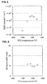
- Example 1 Wafers with the same specifications those in Example 1 were used and subjected to only the RTA treatments under conditions shown in Table 2, followed by heat treatment (800°C, 4 hrs + 1000°C, 16 hrs) to grow oxide precipitates, and thereafter evaluations ( ⁇ Oi, BMD density and DZ layer width) similar to those in Example 1 were performed and shown in graphs of FIGs. 4, 5 and 6.
- Atmosphere Atmosphere Heat treatment temperature Heat treatment time 100% nitrogen 1100°C, 1150°C, 1180°C, 1200°C, 1220°C, 1250°C 30 sec
- the maximum BMD density was increased to 4 to 6.5 ⁇ 10 10 /cm 3 , and the DZ layer width was widened to at least 11 ⁇ m. It was further found that especially at a temperature of post annealing of 900°C to 1050°C, the DZ layer width was a minimum of 15 ⁇ m and increased up to a maximum of 23 ⁇ m.
- a silicon wafer having widened DZ layer width as well as increased BMD density can be manufactured. Moreover, a silicon wafer of the present invention has large BMD density and wide DZ layer width.
Landscapes
- Crystals, And After-Treatments Of Crystals (AREA)
Abstract
Description
| Atmosphere | Heat treatment temperature | Heat treatment time | |
| RTA treatment | 100% nitrogen | 1220° | 30 sec |
| Post annealing | 100 | 700°C, 800°C, 900°C, 950°C, 1000°C, 1050° | 2 hrs |
| Atmosphere Atmosphere | Heat treatment temperature | Heat treatment time | |
| RTA treatment | 100 | 1100°C, 1150°C, 1180°C, 1200°C, 1220°C, 1250° | 30 sec |
| Evaluation items | Results of evaluation |
| ΔOi | 5.1 ppma |
| BMD density | 5.0 × 10¹⁰/cm3 |
| DZ layer width | 23 µm |
| COP density | 0.15 pieces/cm2 |
Claims (9)
- A method for manufacturing a silicon wafer comprising the steps of:performing heat treatment (RTA treatment) to a silicon wafer containing interstitial oxygen with a rapid heating-rapid cooling apparatus, thereby atomic vacancies being injected from a surface of the wafer to form a maximum position of an atomic vacancy concentration in a depth direction in the vicinity of the surface of the wafer; andperforming heat treatment (post annealing) to move the maximum position of the atomic vacancy concentration in the vicinity of the surface of the wafer into the inside of the wafer.
- The method for manufacturing a silicon wafer according to claim 1, wherein the RTA treatment is performed at a temperature higher than an optimal temperature at which an amount of precipitated oxygen or BMD density is maximized.
- The method for manufacturing a silicon wafer according to claim 2, wherein the optimal temperature at which the amount of precipitated oxygen or the BMD density is maximized is determined such that using plural silicon wafers prepared under the same conditions as the silicon wafer containing interstitial oxygen, each wafer thereof is subjected to the RTA treatment at respective plural different temperatures selected in a temperature range of 1100°C to 1350°C, and thereafter oxygen precipitation treatment is applied to the plural silicon wafers subjected to the RTA treatment to obtain a relationship between the amount of precipitated oxygen or the BMD density and an RTA treatment temperature.
- The method for manufacturing a silicon wafer according to any one of claims 1 to 3, wherein the RTA treatment is performed in atmosphere containing nitrogen at a temperature range of 1100 to 1350°C.
- The method for manufacturing a silicon wafer according to any one of claims 1 to 4, wherein the post annealing is performed at a temperature range of 700 to 1050°C.
- The method for manufacturing a silicon wafer according to claim 5, wherein the post annealing performed in the temperature range of 700 to 1050°C is performed by loading a silicon wafer into a heat treatment furnace kept at a specific temperature in the temperature range.
- The method for manufacturing a silicon wafer according to any one of claims 1 to 6, wherein a CZ silicon wafer which has the entire surface composed of an N-region is used as the silicon wafer containing interstitial oxygen.
- A silicon wafer wherein a maximum value of BMD density in the bulk is 4 × 10¹⁰/cm3 or more and DZ layer width is 15 µm or more.
- The silicon wafer according to claim 8, wherein density of COPs of 0.1 µm or more in diameter present on a surface of the silicon wafer is 0.2 pieces/cm2 or less.
Applications Claiming Priority (3)
| Application Number | Priority Date | Filing Date | Title |
|---|---|---|---|
| JP2000325986 | 2000-10-25 | ||
| JP2000325986A JP4106862B2 (en) | 2000-10-25 | 2000-10-25 | Silicon wafer manufacturing method |
| PCT/JP2001/009239 WO2002035599A1 (en) | 2000-10-25 | 2001-10-22 | Production method for silicon wafer and silicon wafer |
Publications (3)
| Publication Number | Publication Date |
|---|---|
| EP1335421A1 true EP1335421A1 (en) | 2003-08-13 |
| EP1335421A4 EP1335421A4 (en) | 2007-08-01 |
| EP1335421B1 EP1335421B1 (en) | 2010-12-29 |
Family
ID=18803262
Family Applications (1)
| Application Number | Title | Priority Date | Filing Date |
|---|---|---|---|
| EP01976791A Expired - Lifetime EP1335421B1 (en) | 2000-10-25 | 2001-10-22 | Production method for silicon wafer |
Country Status (7)
| Country | Link |
|---|---|
| US (1) | US7078357B2 (en) |
| EP (1) | EP1335421B1 (en) |
| JP (1) | JP4106862B2 (en) |
| KR (1) | KR100851127B1 (en) |
| DE (1) | DE60143761D1 (en) |
| TW (1) | TWI282637B (en) |
| WO (1) | WO2002035599A1 (en) |
Cited By (2)
| Publication number | Priority date | Publication date | Assignee | Title |
|---|---|---|---|---|
| EP1975990A4 (en) * | 2006-01-17 | 2009-12-09 | Shinetsu Handotai Kk | METHOD FOR MANUFACTURING SILICON MONOCRYSTAL WAFER |
| CN103003927A (en) * | 2010-07-14 | 2013-03-27 | 信越半导体股份有限公司 | Manufacturing method of silicon substrate and silicon substrate |
Families Citing this family (23)
| Publication number | Priority date | Publication date | Assignee | Title |
|---|---|---|---|---|
| WO2001067503A1 (en) * | 2000-03-03 | 2001-09-13 | Midwest Research Institute | A1 processing for impurity gettering in silicon |
| JP2004063685A (en) * | 2002-07-26 | 2004-02-26 | Matsushita Electric Ind Co Ltd | Method for manufacturing semiconductor device |
| US6955718B2 (en) * | 2003-07-08 | 2005-10-18 | Memc Electronic Materials, Inc. | Process for preparing a stabilized ideal oxygen precipitating silicon wafer |
| KR100531552B1 (en) * | 2003-09-05 | 2005-11-28 | 주식회사 하이닉스반도체 | Silicon wafer and method of fabricating the same |
| CN100461349C (en) * | 2003-10-21 | 2009-02-11 | 株式会社上睦可 | Method for producing high-resistance silicon wafer, epitaxial wafer, and method for producing SOI wafer |
| JP2006261632A (en) * | 2005-02-18 | 2006-09-28 | Sumco Corp | Heat treatment method for silicon wafer |
| JP5239155B2 (en) * | 2006-06-20 | 2013-07-17 | 信越半導体株式会社 | Method for manufacturing silicon wafer |
| DE102007009281B4 (en) * | 2007-02-26 | 2013-03-14 | Infineon Technologies Austria Ag | Method for producing material precipitates and semiconductor material disc and semiconductor components |
| JP5262021B2 (en) * | 2007-08-22 | 2013-08-14 | 株式会社Sumco | Silicon wafer and manufacturing method thereof |
| JPWO2009151077A1 (en) * | 2008-06-10 | 2011-11-17 | 株式会社Sumco | Manufacturing method of silicon single crystal wafer and silicon single crystal wafer |
| JP2010045247A (en) * | 2008-08-14 | 2010-02-25 | Shin Etsu Handotai Co Ltd | Silicon wafer and method of manufacturing silicon wafer |
| US7977216B2 (en) * | 2008-09-29 | 2011-07-12 | Magnachip Semiconductor, Ltd. | Silicon wafer and fabrication method thereof |
| WO2010119614A1 (en) * | 2009-04-13 | 2010-10-21 | 信越半導体株式会社 | Anneal wafer, method for manufacturing anneal wafer, and method for manufacturing device |
| US8999864B2 (en) * | 2009-06-03 | 2015-04-07 | Global Wafers Japan Co., Ltd. | Silicon wafer and method for heat-treating silicon wafer |
| US9945048B2 (en) * | 2012-06-15 | 2018-04-17 | Taiwan Semiconductor Manufacturing Company, Ltd. | Semiconductor structure and method |
| DE102012214085B4 (en) * | 2012-08-08 | 2016-07-07 | Siltronic Ag | Single crystal silicon wafer and process for its production |
| MY188961A (en) * | 2013-07-01 | 2022-01-14 | Solexel Inc | High-throughput thermal processing methods for producing high-efficiency crystalline silicon solar cells |
| US20150187597A1 (en) * | 2013-12-31 | 2015-07-02 | Texas Instruments Incorporated | Method to improve slip resistance of silicon wafers |
| JP6704781B2 (en) * | 2016-04-27 | 2020-06-03 | グローバルウェーハズ・ジャパン株式会社 | Silicon wafer |
| JP6731161B2 (en) * | 2017-04-26 | 2020-07-29 | 信越半導体株式会社 | Method for identifying defect region of silicon single crystal |
| JP6897598B2 (en) * | 2018-02-16 | 2021-06-30 | 信越半導体株式会社 | Heat treatment method for silicon single crystal wafer |
| KR102741720B1 (en) * | 2019-04-16 | 2024-12-11 | 신에쯔 한도타이 가부시키가이샤 | Method for manufacturing silicon single crystal wafer and silicon single crystal wafer |
| US11695048B2 (en) * | 2020-04-09 | 2023-07-04 | Sumco Corporation | Silicon wafer and manufacturing method of the same |
Family Cites Families (11)
| Publication number | Priority date | Publication date | Assignee | Title |
|---|---|---|---|---|
| JPH01242500A (en) * | 1988-03-25 | 1989-09-27 | Mitsubishi Metal Corp | Production of silicon substrate |
| JPH01296628A (en) * | 1988-05-25 | 1989-11-30 | Fujitsu Ltd | Equipment and method for manufacturing semiconductor device |
| IT1242014B (en) * | 1990-11-15 | 1994-02-02 | Memc Electronic Materials | PROCEDURE FOR THE TREATMENT OF SILICON SLICES TO OBTAIN IN IT CONTROLLED PRECIPITATION PROFILES FOR THE PRODUCTION OF ELECTRONIC COMPONENTS. |
| KR0139730B1 (en) * | 1993-02-23 | 1998-06-01 | 사또오 후미오 | Semiconductor substrate and manufacturing method thereof |
| JP2874834B2 (en) | 1994-07-29 | 1999-03-24 | 三菱マテリアル株式会社 | Intrinsic gettering method for silicon wafer |
| JP3085146B2 (en) * | 1995-05-31 | 2000-09-04 | 住友金属工業株式会社 | Silicon single crystal wafer and method of manufacturing the same |
| JP3886576B2 (en) * | 1996-11-06 | 2007-02-28 | 東芝セラミックス株式会社 | Silicon wafer |
| US5994761A (en) | 1997-02-26 | 1999-11-30 | Memc Electronic Materials Spa | Ideal oxygen precipitating silicon wafers and oxygen out-diffusion-less process therefor |
| JP3144631B2 (en) * | 1997-08-08 | 2001-03-12 | 住友金属工業株式会社 | Heat treatment method for silicon semiconductor substrate |
| JP3746153B2 (en) | 1998-06-09 | 2006-02-15 | 信越半導体株式会社 | Heat treatment method for silicon wafer |
| JP3711199B2 (en) | 1998-07-07 | 2005-10-26 | 信越半導体株式会社 | Heat treatment method for silicon substrate |
-
2000
- 2000-10-25 JP JP2000325986A patent/JP4106862B2/en not_active Expired - Lifetime
-
2001
- 2001-10-18 TW TW090125816A patent/TWI282637B/en not_active IP Right Cessation
- 2001-10-22 WO PCT/JP2001/009239 patent/WO2002035599A1/en not_active Ceased
- 2001-10-22 EP EP01976791A patent/EP1335421B1/en not_active Expired - Lifetime
- 2001-10-22 US US10/415,127 patent/US7078357B2/en not_active Expired - Lifetime
- 2001-10-22 DE DE60143761T patent/DE60143761D1/en not_active Expired - Lifetime
- 2001-10-22 KR KR1020037005432A patent/KR100851127B1/en not_active Expired - Fee Related
Cited By (2)
| Publication number | Priority date | Publication date | Assignee | Title |
|---|---|---|---|---|
| EP1975990A4 (en) * | 2006-01-17 | 2009-12-09 | Shinetsu Handotai Kk | METHOD FOR MANUFACTURING SILICON MONOCRYSTAL WAFER |
| CN103003927A (en) * | 2010-07-14 | 2013-03-27 | 信越半导体股份有限公司 | Manufacturing method of silicon substrate and silicon substrate |
Also Published As
| Publication number | Publication date |
|---|---|
| JP2002134515A (en) | 2002-05-10 |
| EP1335421B1 (en) | 2010-12-29 |
| KR100851127B1 (en) | 2008-08-08 |
| DE60143761D1 (en) | 2011-02-10 |
| US20040102056A1 (en) | 2004-05-27 |
| JP4106862B2 (en) | 2008-06-25 |
| EP1335421A4 (en) | 2007-08-01 |
| TWI282637B (en) | 2007-06-11 |
| US7078357B2 (en) | 2006-07-18 |
| KR20030051725A (en) | 2003-06-25 |
| WO2002035599A1 (en) | 2002-05-02 |
Similar Documents
| Publication | Publication Date | Title |
|---|---|---|
| US7078357B2 (en) | Method for manufacturing silicon wafer and silicon wafer | |
| EP2031647B1 (en) | Silicon wafer manufacturing method | |
| US8476149B2 (en) | Method of manufacturing single crystal silicon wafer from ingot grown by Czocharlski process with rapid heating/cooling process | |
| US6843847B1 (en) | Silicon single crystal wafer and production method thereof and soi wafer | |
| EP0962556B1 (en) | Nitrogen doped single crystal silicon wafer with few defects and method for its production | |
| US8187954B2 (en) | Method for manufacturing silicon single crystal wafer | |
| CA2171375C (en) | Manufacturing method of a silicon wafer having a controlled bmd concentration in the bulk and a good dz layer | |
| TWI553173B (en) | An annealing wafer, an annealing wafer, and a method of manufacturing the device | |
| EP0942077B1 (en) | A method for producing a silicon single crystal wafer and a silicon single crystal wafer | |
| JP3407629B2 (en) | Heat treatment method for silicon single crystal wafer and silicon single crystal wafer | |
| US20130093060A1 (en) | Method for producing silicon wafer and silicon wafer | |
| EP0965662B1 (en) | Method for producing low defect silicon single crystal doped with nitrogen | |
| US7189293B2 (en) | Method of producing annealed wafer and annealed wafer | |
| EP1313137A1 (en) | Method for manufacturing single-crystal silicon wafers | |
| EP1975990A1 (en) | Method for manufacturing silicon single crystal wafer | |
| US6204188B1 (en) | Heat treatment method for a silicon wafer and a silicon wafer heat-treated by the method | |
| EP0867928A2 (en) | Heat treatment method for a silicon wafer and a silicon wafer heat-treated by the method | |
| WO2005053010A1 (en) | Annealed wafer and annealed wafer manufacturing method | |
| KR100685260B1 (en) | Heat treatment method of silicon wafer | |
| Storbeck et al. | Denuded Zone Formation by High Temperature Inert Anneal of 300 mm Cz-Silicon Wafers: AEPM: Advanced Equipment, Processes and Materials |
Legal Events
| Date | Code | Title | Description |
|---|---|---|---|
| PUAI | Public reference made under article 153(3) epc to a published international application that has entered the european phase |
Free format text: ORIGINAL CODE: 0009012 |
|
| 17P | Request for examination filed |
Effective date: 20030424 |
|
| AK | Designated contracting states |
Designated state(s): AT BE CH CY DE DK ES FI FR GB GR IE IT LI LU MC NL PT SE TR |
|
| RBV | Designated contracting states (corrected) |
Designated state(s): AT BE CH CY DE FR GB IT LI |
|
| A4 | Supplementary search report drawn up and despatched |
Effective date: 20070702 |
|
| 17Q | First examination report despatched |
Effective date: 20071012 |
|
| RAP1 | Party data changed (applicant data changed or rights of an application transferred) |
Owner name: SHIN-ETSU HANDOTAI CO., LTD. |
|
| GRAP | Despatch of communication of intention to grant a patent |
Free format text: ORIGINAL CODE: EPIDOSNIGR1 |
|
| RTI1 | Title (correction) |
Free format text: PRODUCTION METHOD FOR SILICON WAFER |
|
| RBV | Designated contracting states (corrected) |
Designated state(s): DE FR GB IT |
|
| RIN1 | Information on inventor provided before grant (corrected) |
Inventor name: TOBE, SATOSHI,C/O SHIN-ETSU HANDOTAI CO., LTD Inventor name: AIHARA, KEN,C/O SHIN-ETSU HANDOTAI CO., LTD |
|
| GRAS | Grant fee paid |
Free format text: ORIGINAL CODE: EPIDOSNIGR3 |
|
| GRAA | (expected) grant |
Free format text: ORIGINAL CODE: 0009210 |
|
| AK | Designated contracting states |
Kind code of ref document: B1 Designated state(s): DE FR GB IT |
|
| REG | Reference to a national code |
Ref country code: GB Ref legal event code: FG4D |
|
| REF | Corresponds to: |
Ref document number: 60143761 Country of ref document: DE Date of ref document: 20110210 Kind code of ref document: P |
|
| REG | Reference to a national code |
Ref country code: DE Ref legal event code: R096 Ref document number: 60143761 Country of ref document: DE Effective date: 20110210 |
|
| PLBE | No opposition filed within time limit |
Free format text: ORIGINAL CODE: 0009261 |
|
| STAA | Information on the status of an ep patent application or granted ep patent |
Free format text: STATUS: NO OPPOSITION FILED WITHIN TIME LIMIT |
|
| 26N | No opposition filed |
Effective date: 20110930 |
|
| REG | Reference to a national code |
Ref country code: DE Ref legal event code: R097 Ref document number: 60143761 Country of ref document: DE Effective date: 20110930 |
|
| PG25 | Lapsed in a contracting state [announced via postgrant information from national office to epo] |
Ref country code: IT Free format text: LAPSE BECAUSE OF FAILURE TO SUBMIT A TRANSLATION OF THE DESCRIPTION OR TO PAY THE FEE WITHIN THE PRESCRIBED TIME-LIMIT Effective date: 20101229 |
|
| REG | Reference to a national code |
Ref country code: FR Ref legal event code: ST Effective date: 20120629 |
|
| PG25 | Lapsed in a contracting state [announced via postgrant information from national office to epo] |
Ref country code: FR Free format text: LAPSE BECAUSE OF NON-PAYMENT OF DUE FEES Effective date: 20111102 |
|
| GBPC | Gb: european patent ceased through non-payment of renewal fee |
Effective date: 20121022 |
|
| PG25 | Lapsed in a contracting state [announced via postgrant information from national office to epo] |
Ref country code: GB Free format text: LAPSE BECAUSE OF NON-PAYMENT OF DUE FEES Effective date: 20121022 |
|
| PGFP | Annual fee paid to national office [announced via postgrant information from national office to epo] |
Ref country code: DE Payment date: 20201006 Year of fee payment: 20 |
|
| REG | Reference to a national code |
Ref country code: DE Ref legal event code: R071 Ref document number: 60143761 Country of ref document: DE |