EP1335037A2 - Plasma cvd apparatus - Google Patents
Plasma cvd apparatus Download PDFInfo
- Publication number
- EP1335037A2 EP1335037A2 EP02019104A EP02019104A EP1335037A2 EP 1335037 A2 EP1335037 A2 EP 1335037A2 EP 02019104 A EP02019104 A EP 02019104A EP 02019104 A EP02019104 A EP 02019104A EP 1335037 A2 EP1335037 A2 EP 1335037A2
- Authority
- EP
- European Patent Office
- Prior art keywords
- high frequency
- frequency bias
- semiconductor wafer
- gas
- control signal
- Prior art date
- Legal status (The legal status is an assumption and is not a legal conclusion. Google has not performed a legal analysis and makes no representation as to the accuracy of the status listed.)
- Granted
Links
- 239000007789 gas Substances 0.000 claims abstract description 52
- 239000004065 semiconductor Substances 0.000 claims abstract description 37
- 238000006243 chemical reaction Methods 0.000 claims abstract description 20
- UFHFLCQGNIYNRP-UHFFFAOYSA-N Hydrogen Chemical compound [H][H] UFHFLCQGNIYNRP-UHFFFAOYSA-N 0.000 claims abstract description 19
- 239000001257 hydrogen Substances 0.000 claims abstract description 19
- 229910052739 hydrogen Inorganic materials 0.000 claims abstract description 19
- 238000005268 plasma chemical vapour deposition Methods 0.000 claims abstract description 18
- 238000004544 sputter deposition Methods 0.000 claims abstract description 13
- 239000010409 thin film Substances 0.000 claims abstract description 6
- BLRPTPMANUNPDV-UHFFFAOYSA-N Silane Chemical compound [SiH4] BLRPTPMANUNPDV-UHFFFAOYSA-N 0.000 abstract description 18
- 239000010408 film Substances 0.000 description 19
- 230000015572 biosynthetic process Effects 0.000 description 8
- 238000007740 vapor deposition Methods 0.000 description 5
- 230000006866 deterioration Effects 0.000 description 4
- 230000007423 decrease Effects 0.000 description 3
- 239000000463 material Substances 0.000 description 3
- 239000012808 vapor phase Substances 0.000 description 2
- VYPSYNLAJGMNEJ-UHFFFAOYSA-N Silicium dioxide Chemical compound O=[Si]=O VYPSYNLAJGMNEJ-UHFFFAOYSA-N 0.000 description 1
- 230000002411 adverse Effects 0.000 description 1
- 238000010276 construction Methods 0.000 description 1
- 230000005684 electric field Effects 0.000 description 1
- 230000005284 excitation Effects 0.000 description 1
- 238000004519 manufacturing process Methods 0.000 description 1
- 238000012986 modification Methods 0.000 description 1
- 230000004048 modification Effects 0.000 description 1
- 230000010287 polarization Effects 0.000 description 1
- 229910052814 silicon oxide Inorganic materials 0.000 description 1
- 230000001360 synchronised effect Effects 0.000 description 1
Images


Classifications
-
- C—CHEMISTRY; METALLURGY
- C23—COATING METALLIC MATERIAL; COATING MATERIAL WITH METALLIC MATERIAL; CHEMICAL SURFACE TREATMENT; DIFFUSION TREATMENT OF METALLIC MATERIAL; COATING BY VACUUM EVAPORATION, BY SPUTTERING, BY ION IMPLANTATION OR BY CHEMICAL VAPOUR DEPOSITION, IN GENERAL; INHIBITING CORROSION OF METALLIC MATERIAL OR INCRUSTATION IN GENERAL
- C23C—COATING METALLIC MATERIAL; COATING MATERIAL WITH METALLIC MATERIAL; SURFACE TREATMENT OF METALLIC MATERIAL BY DIFFUSION INTO THE SURFACE, BY CHEMICAL CONVERSION OR SUBSTITUTION; COATING BY VACUUM EVAPORATION, BY SPUTTERING, BY ION IMPLANTATION OR BY CHEMICAL VAPOUR DEPOSITION, IN GENERAL
- C23C16/00—Chemical coating by decomposition of gaseous compounds, without leaving reaction products of surface material in the coating, i.e. chemical vapour deposition [CVD] processes
- C23C16/44—Chemical coating by decomposition of gaseous compounds, without leaving reaction products of surface material in the coating, i.e. chemical vapour deposition [CVD] processes characterised by the method of coating
- C23C16/455—Chemical coating by decomposition of gaseous compounds, without leaving reaction products of surface material in the coating, i.e. chemical vapour deposition [CVD] processes characterised by the method of coating characterised by the method used for introducing gases into reaction chamber or for modifying gas flows in reaction chamber
- C23C16/45523—Pulsed gas flow or change of composition over time
-
- C—CHEMISTRY; METALLURGY
- C23—COATING METALLIC MATERIAL; COATING MATERIAL WITH METALLIC MATERIAL; CHEMICAL SURFACE TREATMENT; DIFFUSION TREATMENT OF METALLIC MATERIAL; COATING BY VACUUM EVAPORATION, BY SPUTTERING, BY ION IMPLANTATION OR BY CHEMICAL VAPOUR DEPOSITION, IN GENERAL; INHIBITING CORROSION OF METALLIC MATERIAL OR INCRUSTATION IN GENERAL
- C23C—COATING METALLIC MATERIAL; COATING MATERIAL WITH METALLIC MATERIAL; SURFACE TREATMENT OF METALLIC MATERIAL BY DIFFUSION INTO THE SURFACE, BY CHEMICAL CONVERSION OR SUBSTITUTION; COATING BY VACUUM EVAPORATION, BY SPUTTERING, BY ION IMPLANTATION OR BY CHEMICAL VAPOUR DEPOSITION, IN GENERAL
- C23C16/00—Chemical coating by decomposition of gaseous compounds, without leaving reaction products of surface material in the coating, i.e. chemical vapour deposition [CVD] processes
- C23C16/22—Chemical coating by decomposition of gaseous compounds, without leaving reaction products of surface material in the coating, i.e. chemical vapour deposition [CVD] processes characterised by the deposition of inorganic material, other than metallic material
- C23C16/30—Deposition of compounds, mixtures or solid solutions, e.g. borides, carbides, nitrides
- C23C16/40—Oxides
- C23C16/401—Oxides containing silicon
- C23C16/402—Silicon dioxide
-
- C—CHEMISTRY; METALLURGY
- C23—COATING METALLIC MATERIAL; COATING MATERIAL WITH METALLIC MATERIAL; CHEMICAL SURFACE TREATMENT; DIFFUSION TREATMENT OF METALLIC MATERIAL; COATING BY VACUUM EVAPORATION, BY SPUTTERING, BY ION IMPLANTATION OR BY CHEMICAL VAPOUR DEPOSITION, IN GENERAL; INHIBITING CORROSION OF METALLIC MATERIAL OR INCRUSTATION IN GENERAL
- C23C—COATING METALLIC MATERIAL; COATING MATERIAL WITH METALLIC MATERIAL; SURFACE TREATMENT OF METALLIC MATERIAL BY DIFFUSION INTO THE SURFACE, BY CHEMICAL CONVERSION OR SUBSTITUTION; COATING BY VACUUM EVAPORATION, BY SPUTTERING, BY ION IMPLANTATION OR BY CHEMICAL VAPOUR DEPOSITION, IN GENERAL
- C23C16/00—Chemical coating by decomposition of gaseous compounds, without leaving reaction products of surface material in the coating, i.e. chemical vapour deposition [CVD] processes
- C23C16/44—Chemical coating by decomposition of gaseous compounds, without leaving reaction products of surface material in the coating, i.e. chemical vapour deposition [CVD] processes characterised by the method of coating
- C23C16/50—Chemical coating by decomposition of gaseous compounds, without leaving reaction products of surface material in the coating, i.e. chemical vapour deposition [CVD] processes characterised by the method of coating using electric discharges
- C23C16/517—Chemical coating by decomposition of gaseous compounds, without leaving reaction products of surface material in the coating, i.e. chemical vapour deposition [CVD] processes characterised by the method of coating using electric discharges using a combination of discharges covered by two or more of groups C23C16/503 - C23C16/515
-
- C—CHEMISTRY; METALLURGY
- C23—COATING METALLIC MATERIAL; COATING MATERIAL WITH METALLIC MATERIAL; CHEMICAL SURFACE TREATMENT; DIFFUSION TREATMENT OF METALLIC MATERIAL; COATING BY VACUUM EVAPORATION, BY SPUTTERING, BY ION IMPLANTATION OR BY CHEMICAL VAPOUR DEPOSITION, IN GENERAL; INHIBITING CORROSION OF METALLIC MATERIAL OR INCRUSTATION IN GENERAL
- C23C—COATING METALLIC MATERIAL; COATING MATERIAL WITH METALLIC MATERIAL; SURFACE TREATMENT OF METALLIC MATERIAL BY DIFFUSION INTO THE SURFACE, BY CHEMICAL CONVERSION OR SUBSTITUTION; COATING BY VACUUM EVAPORATION, BY SPUTTERING, BY ION IMPLANTATION OR BY CHEMICAL VAPOUR DEPOSITION, IN GENERAL
- C23C16/00—Chemical coating by decomposition of gaseous compounds, without leaving reaction products of surface material in the coating, i.e. chemical vapour deposition [CVD] processes
- C23C16/44—Chemical coating by decomposition of gaseous compounds, without leaving reaction products of surface material in the coating, i.e. chemical vapour deposition [CVD] processes characterised by the method of coating
- C23C16/52—Controlling or regulating the coating process
-
- H—ELECTRICITY
- H01—ELECTRIC ELEMENTS
- H01J—ELECTRIC DISCHARGE TUBES OR DISCHARGE LAMPS
- H01J37/00—Discharge tubes with provision for introducing objects or material to be exposed to the discharge, e.g. for the purpose of examination or processing thereof
- H01J37/32—Gas-filled discharge tubes
- H01J37/32009—Arrangements for generation of plasma specially adapted for examination or treatment of objects, e.g. plasma sources
- H01J37/32082—Radio frequency generated discharge
-
- H—ELECTRICITY
- H01—ELECTRIC ELEMENTS
- H01J—ELECTRIC DISCHARGE TUBES OR DISCHARGE LAMPS
- H01J37/00—Discharge tubes with provision for introducing objects or material to be exposed to the discharge, e.g. for the purpose of examination or processing thereof
- H01J37/32—Gas-filled discharge tubes
- H01J37/32431—Constructional details of the reactor
- H01J37/32697—Electrostatic control
- H01J37/32706—Polarising the substrate
Definitions
- the present invention relates to a plasma CVD apparatus which can suppress the deterioration of hydrogen reduction during film formation.
- a plasma CVD apparatus which forms a thin film such as an insulating film on a semiconductor wafer using plasma vapor phase excitation has been conventionally used in semiconductor device manufacturing process.
- This plasma CVD apparatus supplies material gas which consists of elements constituting a thin film onto the, semiconductor wafer and forms a desired thin film by a vapor phase or a chemical reaction on the surface of the semiconductor wafer Plasma discharge is used to excite gas molecules.
- Fig. 4 shows the configuration of a conventional plasma CVD device.
- a reaction container 10 is a container which has an evacuated interior and which allows an insulating film to be formed on a semiconductor wafer 19 having a diameter of 12 inches.
- a nozzle 11 which emits Ar gas, a nozzle 12 which emits O 2 gas and a nozzle 13 which emits SiH 4 gas which serves as the material gas explained above are provided on the inner side face of the reaction container 10.
- An RF electrode 14 is provided on the upper section of the reaction container 10 and connected to a high frequency power supply 15. This RF electrode 14 generates a high frequency electric field to deposit SiO x on the semiconductor wafer 19. As shown in Fig. 5A, during the vapor deposition, an insulating film 19b is formed to cover wirings 19a formed on the semiconductor wafer 19. At this moment, however, the insulating film 19b does not completely reach gaps between the wirings 19a. In Fig. 5A, an RF input is a high frequency input from the RF electrode 14. In addition, the RF power of the RF electrode 14 is set at, for example, 3 kW.
- a support base 16 is provided in the reaction container 10 and supports the semiconductor wafer 19 by an electrostatic force.
- a bias electrode 17 is embedded in the support base 16 so as to be opposed to the RF electrode 14 and is connected to a high frequency power supply 18.
- the bias electrode 17 applies a bias so as to draw ionized Ar + into the semiconductor wafer 19.
- the ionized Ar + etches the insulating film 19b deposited on the upper corner sections of the wirings 19a. In this instance, therefore, the upper sections of the gaps between the wirings 19a are always opened, making it possible to evaporate the insulating film 19b compactly into the gaps between the wirings 19a.
- an LF input is a bias input from the bias electrode 17.
- the bias power of the bias electrode 17 is, for example, 1 kW.
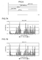
- the Ar gas, the O 2 gas and the SiH 4 gas are constantly emitted from the nozzles 11, 12 and 13 into the reaction container 10, respectively, as can be seen from “B", “C” and “E” shown in Fig. 6.
- the high frequency power supplies 15 and 18 are constantly connected to the RF electrode 14 and the bias electrode 17, respectively. That is; as can be seen from “A” and “D” shown in Fig. 6, the RF electrode 14 and the bias electrode 17 are kept in an RF input (high frequency input) state and an LF input (bias input) state, respectively. Therefore, vapor deposition due to the RF input and sputtering due to the LF input are simultaneously carried out in the reaction container 10.
- the insulating film 19b which consists of SiH 4 is evaporated on the surface of the semiconductor wafer 19 and sputtering is carried out so that Ar + is drawn into the semiconductor wafer 19 side.
- the excess insulating film 19b is scraped off and the insulating film 19b spreads into the gaps between the wirings 19a.
- the conventional plasma CVD apparatus draws Ar + into the semiconductor wafer 19 by applying a bias thereto from the bias electrode 17 shown in Fig. 4. However, when the bias is applied, hydrogen existing in the reaction container 10 is also drawn into the semiconductor wafer 19.
- Fig. 7A is a view which shows a relationship between the mass number of an element and current (drawn-in quantity) when bias is OFF.
- Fig. 7B is a view which shows a relationship between the mass number of an element and current (drawn-in quantity) when bias is ON.
- the mass number of an element 2 corresponds to that of hydrogen molecules (H 2 ).
- the quantity of hydrogen which is drawn into the semiconductor wafer 19 rapidly increases when bias is OFF and ON. In this instance, hydrogen reduction is deteriorated in the semiconductor wafer 19, which adversely influences device characteristic.
- the semiconductor wafer 19 is made of a ferroelectric material, in particular, the P(polarization)-V(applied voltage) characteristic of the semiconductor wafer 19 (semiconductor device) deteriorates as shown in Fig. 8. That is, before film formation, the P-V characteristic has an ordered before-film-formation hysteresis loop 30. After film formation, the P-V characteristic has a disordered after-film-formation hysteresis loop 31.
- the plasma CVD apparatus comprises a reaction container for allowing a reaction for forming a thin film on a semiconductor wafer to be performed, a high frequency bias unit which applies a high frequency bias for sputtering to the semiconductor wafer,'and a high frequency bias control unit which on/off-controls the high frequency bias.
- the plasma CVD apparatus also comprises a gas supply unit which supplies gas containing at least hydrogen to the reaction container, and a gas supply control unit which on/off-controls supply of the gas based on an opposite control logic to a control logic of the high frequency bias control unit.
- Fig. 1 shows the configuration of one embodiment of the apparatus according to the present invention.
- sections corresponding to those shown in Fig. 4 are denoted by the same reference symbols, respectively.
- a flow rate controller 100, a flow rate controller 101, a switch 102 and a control circuit 103 are newly provided.
- the flow rate controller 100 turns on and off the flow rate of O 2 gas emitted from a nozzle 12 based on an O 2 gas flow rate control signal S1 (see Fig. 2B) reversed from the control circuit 103.
- the O 2 gas flow rate control signal S1 shown in Fig. 2B is a signal which is repeatedly turned on and off at predetermined time intervals.
- the flow rate controller 101 turns on and off the flow rate of SiH 4 gas emitted from a nozzle 13 based on an SiH 4 gas flow rate control signal S2 (see Fig. 2C) output from the control circuit 103.
- the SiH 4 gas flow rate control signal S2 shown in Fig. 2C is a signal which is synchronized with the O 2 gas flow rate control signal S1 and which is repeatedly turned on and off at predetermined time intervals.
- the switch 102 is interposed between the bias electrode 17 and the high frequency power supply 18, and is controlled to be turned on and off based on a bias control signal S3 (see Fig. 2D) output from the control circuit 103.
- the bias control signal S3 shown in Fig. 2D is a signal which has a reversed relationship with respect to the O 2 gas flow rate control signal S1 (see Fig. 2B) and the SiH 4 gas flow rate control signal S2 (see Fig. 2C).
- the control circuit 103 outputs the O 2 gas flow rate control signal S1, the SiH 4 gas flow rate control signal S2, and the bias control signal S3 to thereby conduct flow rate control and bias control.
- the O 2 gas flow rate control signal S1 and the SiH 4 gas flow rate control signal S2 are set ON. In this instance, therefore, the O 2 gas and the SiH 4 gas are emitted from the nozzles 12 and 13 into the reaction container 10, respectively. As a result, an insulating film which consists of SiH 4 is evaporated on the surface of the semiconductor wafer 19.
- the bias control signal S3 is set OFF. In this instance, since the bias from the bias electrode 17 is set OFF, sputtering is not carried out.
- the O 2 gas flow rate control signal S1 and the SiH 4 gas flow rate control signal S2 are changed from ON to OFF. Therefore, the emission of O 2 gas and SiH 4 gas from the nozzles 12 and 13 is stopped. In this instance, therefore, no insulating film is evaporated on the semiconductor wafer 19.
- the bias control signal S3 is changed from OFF to ON.
- the bias from the bias electrode 17 is set ON and Ar + is drawn into the semiconductor wafer 19, i.e., sputtering is carried out.
- SiH 4 and the like including hydrogen are not supplied to the reaction container 10, which suppresses unnecessary hydrogen from being drawn into the semiconductor wafer 19. Thereafter, the vapor deposition and the sputtering are alternately repeated at predetermined time intervals.
- Fig. 3 shows the P-V characteristic of the semiconductor wafer 19 in one embodiment of the invention.
- an ordered before-film-formation hysteresis loop 200 and an ordered after-film-formation hysteresis loop 201 are formed, respectively. This represents that the quantity of hydrogen drawn into the semiconductor wafer 19 rapidly decreases in one embodiment of the invention.
- sputtering using the bias is carried out while the supply of SiH 4 gas including hydrogen is stopped. Therefore, rate of drawing originally unnecessary hydrogen into the semiconductor wafer 19 sharply decreases, making it possible to suppress the deterioration of hydrogen reduction in the semiconductor wafer 19 during the film formation.
- control circuit 103 adjusts the switching cycle and the duty ratio between the O 2 gas flow rate control signal S1, the SiH 4 gas flow rate control signal S2, and the bias control signal S3. In this instance, it is possible to minutely control vapor deposition time and sputtering time in accordance with the state of the semiconductor wafer. Further, in one embodiment of the invention, the instance in which the emission of O 2 gas is on/off controlled has been explained. However, since hydrogen is not contained in the O 2 gas in its ideal form, the O 2 gas may be continuously emitted.
- sputtering using the high frequency bias is carried out while the supply of gas including hydrogen is stopped. Therefore, the rate of drawing originally unnecessary' hydrogen into the semiconductor wafer sharply decreases, making it possible to suppress the deterioration of hydrogen reduction in the semiconductor wafer during the film formation.
- the switching cycle and the duty ratio between the high frequency bias control signal and the gas supply control signal are adjusted. It is, therefore, possible to minutely control vapor deposition time and sputtering time in accordance with the state of the semiconductor wafer.
Abstract
Description
- The present invention relates to a plasma CVD apparatus which can suppress the deterioration of hydrogen reduction during film formation.
- A plasma CVD apparatus which forms a thin film such as an insulating film on a semiconductor wafer using plasma vapor phase excitation has been conventionally used in semiconductor device manufacturing process. This plasma CVD apparatus supplies material gas which consists of elements constituting a thin film onto the, semiconductor wafer and forms a desired thin film by a vapor phase or a chemical reaction on the surface of the semiconductor wafer Plasma discharge is used to excite gas molecules.
- Fig. 4 shows the configuration of a conventional plasma CVD device. In Fig. 4, a
reaction container 10 is a container which has an evacuated interior and which allows an insulating film to be formed on asemiconductor wafer 19 having a diameter of 12 inches. Anozzle 11 which emits Ar gas, anozzle 12 which emits O2 gas and anozzle 13 which emits SiH4 gas which serves as the material gas explained above are provided on the inner side face of thereaction container 10. - An
RF electrode 14 is provided on the upper section of thereaction container 10 and connected to a highfrequency power supply 15. ThisRF electrode 14 generates a high frequency electric field to deposit SiOx on thesemiconductor wafer 19. As shown in Fig. 5A, during the vapor deposition, aninsulating film 19b is formed to coverwirings 19a formed on thesemiconductor wafer 19. At this moment, however, theinsulating film 19b does not completely reach gaps between thewirings 19a. In Fig. 5A, an RF input is a high frequency input from theRF electrode 14. In addition, the RF power of theRF electrode 14 is set at, for example, 3 kW. - A
support base 16 is provided in thereaction container 10 and supports thesemiconductor wafer 19 by an electrostatic force. Abias electrode 17 is embedded in thesupport base 16 so as to be opposed to theRF electrode 14 and is connected to a highfrequency power supply 18. - The
bias electrode 17 applies a bias so as to draw ionized Ar+ into thesemiconductor wafer 19. The ionized Ar+ etches theinsulating film 19b deposited on the upper corner sections of thewirings 19a. In this instance, therefore, the upper sections of the gaps between thewirings 19a are always opened, making it possible to evaporate theinsulating film 19b compactly into the gaps between thewirings 19a. In Fig. 5B, an LF input is a bias input from thebias electrode 17. The bias power of thebias electrode 17 is, for example, 1 kW. - According to the configuration explained above, the Ar gas, the O2 gas and the SiH4 gas are constantly emitted from the
nozzles reaction container 10, respectively, as can be seen from "B", "C" and "E" shown in Fig. 6. Likewise, the highfrequency power supplies RF electrode 14 and thebias electrode 17, respectively. That is; as can be seen from "A" and "D" shown in Fig. 6, theRF electrode 14 and thebias electrode 17 are kept in an RF input (high frequency input) state and an LF input (bias input) state, respectively. Therefore, vapor deposition due to the RF input and sputtering due to the LF input are simultaneously carried out in thereaction container 10. - In other words, as shown in Fig. 5B, the
insulating film 19b which consists of SiH4 is evaporated on the surface of thesemiconductor wafer 19 and sputtering is carried out so that Ar+ is drawn into thesemiconductor wafer 19 side. As a result of-this sputtering, -the excessinsulating film 19b is scraped off and theinsulating film 19b spreads into the gaps between thewirings 19a. - The conventional plasma CVD apparatus draws Ar+ into the
semiconductor wafer 19 by applying a bias thereto from thebias electrode 17 shown in Fig. 4. However, when the bias is applied, hydrogen existing in thereaction container 10 is also drawn into thesemiconductor wafer 19. Fig. 7A is a view which shows a relationship between the mass number of an element and current (drawn-in quantity) when bias is OFF. Fig. 7B is a view which shows a relationship between the mass number of an element and current (drawn-in quantity) when bias is ON. The mass number of an element = 2 corresponds to that of hydrogen molecules (H2). - The quantity of hydrogen which is drawn into the
semiconductor wafer 19 rapidly increases when bias is OFF and ON. In this instance, hydrogen reduction is deteriorated in thesemiconductor wafer 19, which adversely influences device characteristic. If thesemiconductor wafer 19 is made of a ferroelectric material, in particular, the P(polarization)-V(applied voltage) characteristic of the semiconductor wafer 19 (semiconductor device) deteriorates as shown in Fig. 8. That is, before film formation, the P-V characteristic has an ordered before-film-formation hysteresis loop 30. After film formation, the P-V characteristic has a disordered after-film-formation hysteresis loop 31. - It is an object of the present invention to provide a plasma CVD apparatus which can suppress the deterioration of hydrogen reduction in a semiconductor wafer during film formation.
- The plasma CVD apparatus according to this invention comprises a reaction container for allowing a reaction for forming a thin film on a semiconductor wafer to be performed, a high frequency bias unit which applies a high frequency bias for sputtering to the semiconductor wafer,'and a high frequency bias control unit which on/off-controls the high frequency bias. The plasma CVD apparatus also comprises a gas supply unit which supplies gas containing at least hydrogen to the reaction container, and a gas supply control unit which on/off-controls supply of the gas based on an opposite control logic to a control logic of the high frequency bias control unit.
- Other objects and features of this invention will become apparent from the following description with reference to the accompanying drawings.
-
- Fig. 1 is a view which shows the configuration of one embodiment of the invention according to the present invention,
- Fig. 2A to Fig. 2D are timing charts which explain various gas outputs, an RF input and an LF input in the embodiment of the invention,
- Fig. 3 is a view which shows P-V characteristic in the embodiment of the invention,
- Fig. 4 is a view which shows the configuration of a conventional plasma CVD apparatus,
- Fig. 5A and Fig. 5B are views which explain film formation in the conventional plasma CVD apparatus,
- Fig. 6 is a timing chart which explains various gas outputs, an RF input, and an LF input in the conventional plasma CVD apparatus,
- Fig. 7A and Fig. 7B are views which explain the problems of the conventional plasma CVD apparatus, and
- Fig. 8 is a view which shows the P-V characteristic of the conventional plasma CVD apparatus.
-
- An embodiment of the plasma CVD apparatus according to the present invention will be explained hereinafter in detail with reference to the drawings.
- Fig. 1 shows the configuration of one embodiment of the apparatus according to the present invention. In Fig. 1, sections corresponding to those shown in Fig. 4 are denoted by the same reference symbols, respectively. In Fig. 1, a
flow rate controller 100, aflow rate controller 101, aswitch 102 and acontrol circuit 103 are newly provided. - The
flow rate controller 100 turns on and off the flow rate of O2 gas emitted from anozzle 12 based on an O2 gas flow rate control signal S1 (see Fig. 2B) reversed from thecontrol circuit 103. The O2 gas flow rate control signal S1 shown in Fig. 2B is a signal which is repeatedly turned on and off at predetermined time intervals. - The
flow rate controller 101 turns on and off the flow rate of SiH4 gas emitted from anozzle 13 based on an SiH4 gas flow rate control signal S2 (see Fig. 2C) output from thecontrol circuit 103. The SiH4 gas flow rate control signal S2 shown in Fig. 2C is a signal which is synchronized with the O2 gas flow rate control signal S1 and which is repeatedly turned on and off at predetermined time intervals. - The
switch 102 is interposed between thebias electrode 17 and the highfrequency power supply 18, and is controlled to be turned on and off based on a bias control signal S3 (see Fig. 2D) output from thecontrol circuit 103. The bias control signal S3 shown in Fig. 2D is a signal which has a reversed relationship with respect to the O2 gas flow rate control signal S1 (see Fig. 2B) and the SiH4 gas flow rate control signal S2 (see Fig. 2C). Thecontrol circuit 103 outputs the O2 gas flow rate control signal S1, the SiH4 gas flow rate control signal S2, and the bias control signal S3 to thereby conduct flow rate control and bias control. - As the line "B" in Fig. 2A indicates that Ar gas is constantly emitted from the
nozzle 11 into thereaction container 10. Similarly, the line "A" in Fig. 2A indicates that the highfrequency power supply 15 is constantly connected to theRF electrode 14. - Between time t0 and time t1 (e.g., for 20 sec) shown in Fig. 2B to Fig. 2C, the O2 gas flow rate control signal S1 and the SiH4 gas flow rate control signal S2 are set ON. In this instance, therefore, the O2 gas and the SiH4 gas are emitted from the
nozzles reaction container 10, respectively. As a result, an insulating film which consists of SiH4 is evaporated on the surface of thesemiconductor wafer 19. - On the other hand, between time t0 and time t1 shown in Fig. 2D, the bias control signal S3 is set OFF. In this instance, since the bias from the
bias electrode 17 is set OFF, sputtering is not carried out. - Between time t1 and time t2, the O2 gas flow rate control signal S1 and the SiH4 gas flow rate control signal S2 are changed from ON to OFF. Therefore, the emission of O2 gas and SiH4 gas from the
nozzles semiconductor wafer 19. - On the other hand, between time t1 and time t2, the bias control signal S3 is changed from OFF to ON. In this instance, therefore, the bias from the
bias electrode 17 is set ON and Ar+ is drawn into thesemiconductor wafer 19, i.e., sputtering is carried out. In this instance, SiH4 and the like including hydrogen are not supplied to thereaction container 10, which suppresses unnecessary hydrogen from being drawn into thesemiconductor wafer 19. Thereafter, the vapor deposition and the sputtering are alternately repeated at predetermined time intervals. - Fig. 3 shows the P-V characteristic of the
semiconductor wafer 19 in one embodiment of the invention. As can be seen from Fig. 3, before and after film formation, an ordered before-film-formation hysteresis loop 200 and an ordered after-film-formation hysteresis loop 201 are formed, respectively. This represents that the quantity of hydrogen drawn into thesemiconductor wafer 19 rapidly decreases in one embodiment of the invention. - According to one- embodiment of the invention, sputtering using the bias is carried out while the supply of SiH4 gas including hydrogen is stopped. Therefore, rate of drawing originally unnecessary hydrogen into the
semiconductor wafer 19 sharply decreases, making it possible to suppress the deterioration of hydrogen reduction in thesemiconductor wafer 19 during the film formation. - Note that it is possible that the
control circuit 103 adjusts the switching cycle and the duty ratio between the O2 gas flow rate control signal S1, the SiH4 gas flow rate control signal S2, and the bias control signal S3. In this instance, it is possible to minutely control vapor deposition time and sputtering time in accordance with the state of the semiconductor wafer. Further, in one embodiment of the invention, the instance in which the emission of O2 gas is on/off controlled has been explained. However, since hydrogen is not contained in the O2 gas in its ideal form, the O2 gas may be continuously emitted. - According to the present invention, sputtering using the high frequency bias is carried out while the supply of gas including hydrogen is stopped. Therefore, the rate of drawing originally unnecessary' hydrogen into the semiconductor wafer sharply decreases, making it possible to suppress the deterioration of hydrogen reduction in the semiconductor wafer during the film formation.
- Moreover, the switching cycle and the duty ratio between the high frequency bias control signal and the gas supply control signal are adjusted. It is, therefore, possible to minutely control vapor deposition time and sputtering time in accordance with the state of the semiconductor wafer.
- Although the invention has been described with respect to a specific embodiment for a complete and clear disclosure, the appended claims are not to be thus limited but are to be construed as embodying all modifications and alternative constructions that may occur to one skilled in the art which fairly fall within the basic teaching herein set forth.
Claims (3)
- A plasma CVD apparatus comprising:a reaction container for allowing a reaction for forming a thin film on a semiconductor wafer to be performed;a high frequency bias unit which applies a high frequency bias for sputtering to the semiconductor wafer;a high frequency bias control unit which on/off-controls the high frequency bias;a gas supply unit which supplies gas containing at least hydrogen to the reaction container; anda gas supply control unit which on/off-controls supply of the gas based on an opposite control logic to a control logic of the high frequency bias control unit.
- The plasma CVD apparatus according to claim 1, wherein
the high frequency bias control unit conducts control based on a high frequency bias control signal repeatedly turned on and off at predetermined time intervals, and
the gas supply control unit conducts control based on a gas supply control signal in a reversed relationship with the high frequency bias control signal. - The plasma CVD apparatus according to claim 2, comprising an adjustment unit which adjusts a switching cycle and a duty ratio between the high frequency bias control signal and the gas supply control signal.
Applications Claiming Priority (2)
| Application Number | Priority Date | Filing Date | Title |
|---|---|---|---|
| JP2002025606 | 2002-02-01 | ||
| JP2002025606A JP3836032B2 (en) | 2002-02-01 | 2002-02-01 | Plasma CVD equipment |
Publications (3)
| Publication Number | Publication Date |
|---|---|
| EP1335037A2 true EP1335037A2 (en) | 2003-08-13 |
| EP1335037A3 EP1335037A3 (en) | 2004-09-01 |
| EP1335037B1 EP1335037B1 (en) | 2005-07-27 |
Family
ID=27606469
Family Applications (1)
| Application Number | Title | Priority Date | Filing Date |
|---|---|---|---|
| EP02019104A Expired - Fee Related EP1335037B1 (en) | 2002-02-01 | 2002-08-29 | Plasma cvd apparatus |
Country Status (6)
| Country | Link |
|---|---|
| US (1) | US7314525B2 (en) |
| EP (1) | EP1335037B1 (en) |
| JP (1) | JP3836032B2 (en) |
| KR (1) | KR100514670B1 (en) |
| DE (1) | DE60205210T2 (en) |
| TW (1) | TW557479B (en) |
Families Citing this family (2)
| Publication number | Priority date | Publication date | Assignee | Title |
|---|---|---|---|---|
| DE502005001749D1 (en) * | 2005-07-28 | 2007-11-29 | Applied Materials Gmbh & Co Kg | Vapor deposition |
| JP5022116B2 (en) * | 2007-06-18 | 2012-09-12 | 三菱重工業株式会社 | Semiconductor device manufacturing method and manufacturing apparatus |
Citations (4)
| Publication number | Priority date | Publication date | Assignee | Title |
|---|---|---|---|---|
| US6028014A (en) * | 1997-11-10 | 2000-02-22 | Lsi Logic Corporation | Plasma-enhanced oxide process optimization and material and apparatus therefor |
| US6326064B1 (en) * | 1991-05-17 | 2001-12-04 | Lam Research Corporation | Process for depositing a SiOx film having reduced intrinsic stress and/or reduced hydrogen content |
| EP1302561A1 (en) * | 1998-04-21 | 2003-04-16 | Applied Materials, Inc. | Method and apparatus for forming a layer on a substrate by high-density plasma chemical vapor deposition (HDP-CVD) |
| US6566186B1 (en) * | 2000-05-17 | 2003-05-20 | Lsi Logic Corporation | Capacitor with stoichiometrically adjusted dielectric and method of fabricating same |
Family Cites Families (9)
| Publication number | Priority date | Publication date | Assignee | Title |
|---|---|---|---|---|
| JPH06216047A (en) | 1993-01-12 | 1994-08-05 | Anelva Corp | Microwave plasma cvd film formation and device therefor |
| US5494522A (en) * | 1993-03-17 | 1996-02-27 | Tokyo Electron Limited | Plasma process system and method |
| JP2783276B2 (en) | 1995-07-04 | 1998-08-06 | 日本電気株式会社 | Method for manufacturing semiconductor device |
| JP2915357B2 (en) | 1996-03-06 | 1999-07-05 | 松下電器産業株式会社 | Semiconductor device, method of manufacturing the same, and method of forming porous film |
| JP3325793B2 (en) | 1996-03-22 | 2002-09-17 | 三洋電機株式会社 | Amorphous semiconductor, method for manufacturing the same, and photovoltaic device |
| JP3429171B2 (en) * | 1997-11-20 | 2003-07-22 | 東京エレクトロン株式会社 | Plasma processing method and semiconductor device manufacturing method |
| EP1071833B1 (en) | 1998-04-21 | 2005-09-07 | Applied Materials, Inc. | Method and apparatus for modifying the profile of high-aspect-ratio gaps using differential plasma power |
| JP2000306696A (en) * | 1999-04-21 | 2000-11-02 | Shimadzu Corp | Ecr plasma device |
| JP2001267310A (en) | 2000-03-17 | 2001-09-28 | Tokyo Electron Ltd | Method and device for film forming plasma |
-
2002
- 2002-02-01 JP JP2002025606A patent/JP3836032B2/en not_active Expired - Fee Related
- 2002-07-24 US US10/201,020 patent/US7314525B2/en not_active Expired - Lifetime
- 2002-07-30 TW TW091117021A patent/TW557479B/en not_active IP Right Cessation
- 2002-08-29 EP EP02019104A patent/EP1335037B1/en not_active Expired - Fee Related
- 2002-08-29 DE DE60205210T patent/DE60205210T2/en not_active Expired - Fee Related
-
2003
- 2003-01-29 KR KR10-2003-0005696A patent/KR100514670B1/en not_active IP Right Cessation
Patent Citations (4)
| Publication number | Priority date | Publication date | Assignee | Title |
|---|---|---|---|---|
| US6326064B1 (en) * | 1991-05-17 | 2001-12-04 | Lam Research Corporation | Process for depositing a SiOx film having reduced intrinsic stress and/or reduced hydrogen content |
| US6028014A (en) * | 1997-11-10 | 2000-02-22 | Lsi Logic Corporation | Plasma-enhanced oxide process optimization and material and apparatus therefor |
| EP1302561A1 (en) * | 1998-04-21 | 2003-04-16 | Applied Materials, Inc. | Method and apparatus for forming a layer on a substrate by high-density plasma chemical vapor deposition (HDP-CVD) |
| US6566186B1 (en) * | 2000-05-17 | 2003-05-20 | Lsi Logic Corporation | Capacitor with stoichiometrically adjusted dielectric and method of fabricating same |
Also Published As
| Publication number | Publication date |
|---|---|
| EP1335037B1 (en) | 2005-07-27 |
| US20030145788A1 (en) | 2003-08-07 |
| JP2003226980A (en) | 2003-08-15 |
| KR20030066357A (en) | 2003-08-09 |
| US7314525B2 (en) | 2008-01-01 |
| DE60205210T2 (en) | 2006-05-24 |
| JP3836032B2 (en) | 2006-10-18 |
| TW557479B (en) | 2003-10-11 |
| KR100514670B1 (en) | 2005-09-13 |
| DE60205210D1 (en) | 2005-09-01 |
| EP1335037A3 (en) | 2004-09-01 |
Similar Documents
| Publication | Publication Date | Title |
|---|---|---|
| TWI588889B (en) | Plasma processing method and plasma processing device | |
| KR101993880B1 (en) | Plasma-treatment apparatus | |
| US10056230B2 (en) | Power supply system, plasma processing apparatus and power supply control method | |
| US6610169B2 (en) | Semiconductor processing system and method | |
| US5437895A (en) | Plasma CVD process for forming amorphous silicon thin film | |
| US20050126712A1 (en) | Plasma processing method | |
| US20120145186A1 (en) | Plasma processing apparatus | |
| US20080317965A1 (en) | Plasma processing apparatus and method | |
| US20020123237A1 (en) | Plasma pulse semiconductor processing system and method | |
| JP4714166B2 (en) | Substrate plasma processing apparatus and plasma processing method | |
| US8545671B2 (en) | Plasma processing method and plasma processing apparatus | |
| EP0670666B1 (en) | Plasma generating apparatus and plasma processing apparatus | |
| US7223449B2 (en) | Film deposition method | |
| US5262001A (en) | Dry etching method for perovskite oxide film | |
| US20070020898A1 (en) | System and method for semiconductor processing | |
| US20110247995A1 (en) | Dry etching method and dry etching apparatus | |
| EP1335037B1 (en) | Plasma cvd apparatus | |
| US9548214B2 (en) | Plasma etching method of modulating high frequency bias power to processing target object | |
| KR20220044295A (en) | Three-step pulsing system and method for plasma process | |
| US6223686B1 (en) | Apparatus for forming a thin film by plasma chemical vapor deposition | |
| US6153268A (en) | Method for producing oriented piezoelectric films | |
| US6060131A (en) | Method of forming a thin film by plasma chemical vapor deposition | |
| JP2011084769A (en) | Method for producing thin-film element, film-forming apparatus, and method for operating the same | |
| JP2006089833A (en) | Ecr sputtering apparatus | |
| JPS63156536A (en) | Reactive plasma beam film forming device |
Legal Events
| Date | Code | Title | Description |
|---|---|---|---|
| PUAI | Public reference made under article 153(3) epc to a published international application that has entered the european phase |
Free format text: ORIGINAL CODE: 0009012 |
|
| 17P | Request for examination filed |
Effective date: 20020829 |
|
| AK | Designated contracting states |
Designated state(s): AT BE BG CH CY CZ DE DK EE ES FI FR GB GR IE IT LI LU MC NL PT SE SK TR |
|
| AX | Request for extension of the european patent |
Extension state: AL LT LV MK RO SI |
|
| PUAL | Search report despatched |
Free format text: ORIGINAL CODE: 0009013 |
|
| AK | Designated contracting states |
Kind code of ref document: A3 Designated state(s): AT BE BG CH CY CZ DE DK EE ES FI FR GB GR IE IT LI LU MC NL PT SE SK TR |
|
| AX | Request for extension of the european patent |
Extension state: AL LT LV MK RO SI |
|
| GRAP | Despatch of communication of intention to grant a patent |
Free format text: ORIGINAL CODE: EPIDOSNIGR1 |
|
| GRAS | Grant fee paid |
Free format text: ORIGINAL CODE: EPIDOSNIGR3 |
|
| AKX | Designation fees paid |
Designated state(s): DE FR GB |
|
| GRAA | (expected) grant |
Free format text: ORIGINAL CODE: 0009210 |
|
| AK | Designated contracting states |
Kind code of ref document: B1 Designated state(s): DE FR GB |
|
| REG | Reference to a national code |
Ref country code: GB Ref legal event code: FG4D |
|
| RIN1 | Information on inventor provided before grant (corrected) |
Inventor name: SHIMAZU, TADASHI,TAKASAGO RES. & DEV. CENTER Inventor name: INOUE, MASAHIKO,KOBE SHIPYARD & MACHINERY WORK |
|
| REF | Corresponds to: |
Ref document number: 60205210 Country of ref document: DE Date of ref document: 20050901 Kind code of ref document: P |
|
| ET | Fr: translation filed | ||
| PLBE | No opposition filed within time limit |
Free format text: ORIGINAL CODE: 0009261 |
|
| STAA | Information on the status of an ep patent application or granted ep patent |
Free format text: STATUS: NO OPPOSITION FILED WITHIN TIME LIMIT |
|
| 26N | No opposition filed |
Effective date: 20060428 |
|
| PGFP | Annual fee paid to national office [announced via postgrant information from national office to epo] |
Ref country code: FR Payment date: 20060808 Year of fee payment: 5 |
|
| PGFP | Annual fee paid to national office [announced via postgrant information from national office to epo] |
Ref country code: GB Payment date: 20060823 Year of fee payment: 5 |
|
| PGFP | Annual fee paid to national office [announced via postgrant information from national office to epo] |
Ref country code: DE Payment date: 20060824 Year of fee payment: 5 |
|
| GBPC | Gb: european patent ceased through non-payment of renewal fee |
Effective date: 20070829 |
|
| REG | Reference to a national code |
Ref country code: FR Ref legal event code: ST Effective date: 20080430 |
|
| PG25 | Lapsed in a contracting state [announced via postgrant information from national office to epo] |
Ref country code: DE Free format text: LAPSE BECAUSE OF NON-PAYMENT OF DUE FEES Effective date: 20080301 |
|
| PG25 | Lapsed in a contracting state [announced via postgrant information from national office to epo] |
Ref country code: FR Free format text: LAPSE BECAUSE OF NON-PAYMENT OF DUE FEES Effective date: 20070831 |
|
| PG25 | Lapsed in a contracting state [announced via postgrant information from national office to epo] |
Ref country code: GB Free format text: LAPSE BECAUSE OF NON-PAYMENT OF DUE FEES Effective date: 20070829 |