EP1333610A2 - Taktregelungsschaltung zur Taktphasenregelung eines Transceivers - Google Patents
Taktregelungsschaltung zur Taktphasenregelung eines Transceivers Download PDFInfo
- Publication number
- EP1333610A2 EP1333610A2 EP03000410A EP03000410A EP1333610A2 EP 1333610 A2 EP1333610 A2 EP 1333610A2 EP 03000410 A EP03000410 A EP 03000410A EP 03000410 A EP03000410 A EP 03000410A EP 1333610 A2 EP1333610 A2 EP 1333610A2
- Authority
- EP
- European Patent Office
- Prior art keywords
- signal
- phase
- control circuit
- clock
- circuit
- Prior art date
- Legal status (The legal status is an assumption and is not a legal conclusion. Google has not performed a legal analysis and makes no representation as to the accuracy of the status listed.)
- Withdrawn
Links
- 238000005070 sampling Methods 0.000 claims abstract description 64
- 230000005540 biological transmission Effects 0.000 claims description 40
- 238000012544 monitoring process Methods 0.000 claims description 10
- 238000012935 Averaging Methods 0.000 claims description 8
- 238000001914 filtration Methods 0.000 claims description 4
- 230000001681 protective effect Effects 0.000 claims description 2
- 230000001105 regulatory effect Effects 0.000 description 5
- 230000001419 dependent effect Effects 0.000 description 4
- 230000033228 biological regulation Effects 0.000 description 3
- 238000000034 method Methods 0.000 description 3
- 230000001276 controlling effect Effects 0.000 description 2
- 230000008878 coupling Effects 0.000 description 2
- 238000010168 coupling process Methods 0.000 description 2
- 238000005859 coupling reaction Methods 0.000 description 2
- 230000003247 decreasing effect Effects 0.000 description 2
- 238000012545 processing Methods 0.000 description 2
- 230000000630 rising effect Effects 0.000 description 2
- 230000001360 synchronised effect Effects 0.000 description 2
- 238000012546 transfer Methods 0.000 description 2
- RYGMFSIKBFXOCR-UHFFFAOYSA-N Copper Chemical compound [Cu] RYGMFSIKBFXOCR-UHFFFAOYSA-N 0.000 description 1
- 230000003044 adaptive effect Effects 0.000 description 1
- 239000002131 composite material Substances 0.000 description 1
- 229910052802 copper Inorganic materials 0.000 description 1
- 239000010949 copper Substances 0.000 description 1
- 238000010586 diagram Methods 0.000 description 1
- 230000009123 feedback regulation Effects 0.000 description 1
- 230000010363 phase shift Effects 0.000 description 1
- 230000002123 temporal effect Effects 0.000 description 1
Images


Classifications
-
- H—ELECTRICITY
- H04—ELECTRIC COMMUNICATION TECHNIQUE
- H04L—TRANSMISSION OF DIGITAL INFORMATION, e.g. TELEGRAPHIC COMMUNICATION
- H04L7/00—Arrangements for synchronising receiver with transmitter
- H04L7/0016—Arrangements for synchronising receiver with transmitter correction of synchronization errors
- H04L7/002—Arrangements for synchronising receiver with transmitter correction of synchronization errors correction by interpolation
- H04L7/0029—Arrangements for synchronising receiver with transmitter correction of synchronization errors correction by interpolation interpolation of received data signal
-
- H—ELECTRICITY
- H04—ELECTRIC COMMUNICATION TECHNIQUE
- H04B—TRANSMISSION
- H04B3/00—Line transmission systems
- H04B3/02—Details
- H04B3/20—Reducing echo effects or singing; Opening or closing transmitting path; Conditioning for transmission in one direction or the other
- H04B3/23—Reducing echo effects or singing; Opening or closing transmitting path; Conditioning for transmission in one direction or the other using a replica of transmitted signal in the time domain, e.g. echo cancellers
-
- H—ELECTRICITY
- H04—ELECTRIC COMMUNICATION TECHNIQUE
- H04L—TRANSMISSION OF DIGITAL INFORMATION, e.g. TELEGRAPHIC COMMUNICATION
- H04L7/00—Arrangements for synchronising receiver with transmitter
- H04L7/0054—Detection of the synchronisation error by features other than the received signal transition
- H04L7/0058—Detection of the synchronisation error by features other than the received signal transition detection of error based on equalizer tap values
-
- H—ELECTRICITY
- H04—ELECTRIC COMMUNICATION TECHNIQUE
- H04L—TRANSMISSION OF DIGITAL INFORMATION, e.g. TELEGRAPHIC COMMUNICATION
- H04L7/00—Arrangements for synchronising receiver with transmitter
- H04L7/0054—Detection of the synchronisation error by features other than the received signal transition
- H04L7/0062—Detection of the synchronisation error by features other than the received signal transition detection of error based on data decision error, e.g. Mueller type detection
Definitions
- the invention relates to a clock phase control circuit for Clock phase control of a transceiver according to the generic term of claim 1.
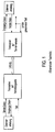
- Fig. 1 shows a data transmission system according to the prior art of the technique.
- a transceiver or a transmit and receive circuit receives and sends transmission data from a data source this as an analog transmission signal via a data transmission line to another transceiver.
- the data transmission line it is, for example, a two-wire telephone line made of copper.
- the transceiver on the switching side COT central office terminal
- the transceiver on the switching side COT central office terminal
- the transceiver on the switching side COT central office terminal
- the transceiver on the switching side COT central office terminal
- the transceiver on the subscriber side RT forms the so-called clock slave, i.e. the receiving end recovered clock signal is used as its send clock.
- the clock control circuit of the exchange side Transceivers only the exact sampling phase in the contained therein Set the receiver. The sampling phase depends on this everything depends on the signal runtime of the transmission line.
- the analog Received signal from a transceiver is made up of two Signal components together, namely from the opposite Transceiver broadcast signal and from the signal component coupled in from the own transmitting device or the echo signal component.
- the echo signal component provides is a signal interference and is in the receiver of the transceiver compensated by an echo cancellation circuit.
- the echo cancellation circuit within the transceiver is calculated the most accurate possible estimate for the Echo signal component and subtracts this from the received Signal.
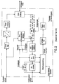
- Fig. 2 shows a conventional prior art transceiver of the technique.
- the transceiver consists of a transmit signal path and a receive signal path.
- the transmission data or transmission data symbols are first a transmission filter in the transmission signal path fed and then by means of a digital analog converter converted into an analog broadcast signal.
- the analog Transmit signal is amplified with a driver circuit submitted a hybrid hybrid.
- the hybrid hybrid system is connected to the data transmission line.
- the received analog signal is initially on the received signal path filtered by an analog receive filter EF and then sampled.
- the scanning takes place within a Sampling circuit, either from an analog to digital converter consists or, as shown in Fig. 2, of an analog-digital converter, an interpolation filter IF and a downstream one Interpolator.
- the analog-digital converter gropes the analog received signal with a free-running working clock signal from.
- the sampled signal is then fed to the digital interpolation filter IF and through the Interpolator interpolates. For this, the interpolator is used regulated sampling clock signal supplied.
- a subtraction circuit A is connected downstream of the sampling circuit, that of the sampled digital received signal the estimation signal calculated by the echo cancellation circuit by generating an echo-compensated digital Received signal subtracted.
- the echo cancellation circuit calculates the expected data based on the received data symbols Echo signal and subtracts this from the received Signal.
- the echo cancellation circuit is usually adaptively adjustable. The echo cancellation circuit becomes adaptive depending on the transmission function of the transmission line and the analog components such as the transmitter, set.
- the difference signal formed by the subtractor A becomes one Amplitude control circuit AGC (Automatic Gain Control) fed.
- AGC Automatic Gain Control
- the digital received signal regulated in amplitude is then equalized by an equalizer.
- the downstream decision maker determines from the equalized received signal an estimate of that originally from the other Transceiver broadcast data icon.
- the won Send data symbol is used for further data processing by delivered to the transceiver to the data sink.
- a subtractor makes a difference between the signal values before and after Decision maker by.
- This error or deviation signal serves as a setting signal for the echo cancellation circuit.
- the echo canceller either the subtractor A formed differential signal or that of Subtractor B formed differential signal can be used. Switching between the two setting options takes place by means of a switch.
- a clock control criterion or a by means of a control circuit Clock control signal For the regulation of the sampling phase of the received signal a clock control criterion or a by means of a control circuit Clock control signal generated.
- the timing control signal gives the phase deviation between the signal phase of the sampling clock signal and a desired target signal phase of an ideal one Sampling clock signal.
- the clock control criterion or the clock control signal is a measure of the phase error between the ideal sampling clock at which a maximum signal-to-noise ratio and the actual sampling clock.
- the timing control signal is generated from the samples before and after Decision-makers (decision-feedback regulation) and further from at least one of the coefficients of the linear equalizer EQ generated by the control circuit.
- the timing rule criterion or the timing control signal exposes itself two parts together, namely one signal part, the depends on the samples before and after the decision maker, and from a second signal component, which is both dependent of one or more coefficients of the linear equalizer as well as from a suitably specified one and to the control circuit applied phase reference signal value.
- the signal component is correct is dependent on the coefficient with the predetermined phase reference signal value match.
- the control circuit generates hence a tax variable that is a measure of the deviation represents the sampling phase from the target phase.
- the generated clock control signal is sent to a digital Loop filter delivered.
- the output signal of the loop filter directly controls the sampling phase of the sampling clock signal for the sampling circuit. This is usually done with a Realized phase counter.
- the counter reading of the phase counter defines the phase difference between the transmit and the reception phase. In the steady state the counter reading of the phase counter largely constant accordingly the constant phase difference between the phases of the transmission signal and the phase of the reception signal. This constant phase difference depends on the signal transit time Transmission line.
- the reception phase or the Phase of the digital received signal compared to the phase of the Transmitted signal changed. Since the coupled echo signal with the phase of the broadcast signal is received at each Clock phase adjustment also that sampled with the reception clock Echo signal also changed.
- the transceiver on the switching side therefore has a strong coupling of the clock phase control circuit with the echo cancellation circuit EC on. After the phase change is the echo cancellation circuit again and the equalizer EQ must be like this be resynchronized as far as possible.
- the invention provides a clock phase control circuit for clock phase control of a transceiver a sampling circuit for sampling an analog received signal with a sampling clock signal, an echo signal compensation circuit for compensating an echo signal which is caused by a transmission signal transmitted by the transceiver, the echo signal compensation circuit being adaptively adjustable as a function of a setting signal, a control circuit for generating a control signal for clock phase control, which indicates the phase deviation between the signal phase of the sampling clock signal and a desired signal phase of an ideal sampling clock signal, a loop filter for filtering the control signal, a phase counter for generating the sampling clock signal as a function of the filtered control signal, the clock phase control circuit according to the invention being characterized in that that an amplitude limiting circuit is provided between the loop filter and the phase counter, which limits the amplitude of the filtered control signal to a limiting value, the limit value depends on the setting signal for the echo signal compensation circuit.
- the sampling circuit contains an analog-digital converter for converting the analog received signal into a digital received signal, a digital interpolation filter for filtering the digital received signal and an interpolator for interpolating the filtered digital received signal.
- the analog-digital converter is preferably replaced by a free-running working clock signal clocked.
- the interpolator is preferably controlled by the sampling clock signal clocked.
- a digital output signal of the echo signal compensation circuit is preferably from the filtered digital Received signal by means of a subtractor to generate a echo-compensated digital received signal subtracted.
- Clock phase control circuit is an amplitude control circuit for amplitude control of the echo-compensated digital Received signal provided.
- Clock phase control circuit is an equalizer for signal equalization of the echo-compensated digital Received signal provided.
- the equalizer is one linear equalizer.
- the equalizer is a decision feedback equalizer.
- a decision-maker is preferably connected downstream of the equalizer, the one from the equalized digital received signal Estimated value for the received signal generated.
- a subtractor is provided, the generated by the equalized digital received signal Subtracted estimate to form a difference signal, which for setting the echo signal compensation circuit is provided.
- the timing circuit calculates the control circuit the time-averaged phase deviation between the phase of the sampling signal and a phase reference value Generation of a phase deviation signal.
- a controllable amplifier is preferably also provided, which the phase deviation signal depending on a gain setting signal for generating the setting signal amplified for the echo cancellation circuit.
- the gain adjustment signal is preferably provided by the amplitude control circuit generated.
- the limit value for the amplitude limiting circuit is preferably dependent on a calculation circuit from the setting signal for the echo cancellation circuit calculated, with increasing setting signal value the limit value is increased.
- a protective circuit is additionally provided to avoid mis-synchronization, which contains an amount calculation circuit for generating the amount of the difference signal, a downstream averaging filter and a monitoring control circuit, the monitoring control circuit controlling a phase counter for adjusting the phase of the scanning signal by a predetermined phase jump value , if the difference signal averaged by the averaging filter does not fall below an adjustable threshold value for a certain period of time.
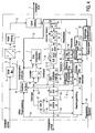
- Fig. 3 shows a transceiver 1, the inventive Includes clock phase control circuit.
- the transceiver 1 is via a hybrid hybrid circuit 2 to a data transmission line 3 connected. Via the data transmission line 3 the transceiver 1 receives an analog receive signal from another transceiver. The transceiver also transmits 1 a separate transmission signal via the data transmission line 3.
- the transceiver 1 consists of a transmission signal path and a Receive signal path.
- the transceiver 1 receives via a data line 4 from a data source transmit data symbols that a digital transmission filter 5 are supplied.
- the incoming Send data symbols are also sent via a line 6 to a echo compensation circuit 7 contained in the transceiver 1 created.
- the transmission filter 5 is a digital-to-analog converter via a line 8 9 downstream.
- the digital-to-analog converter 9 converts the filtered transmission data into an analog transmission signal um and passes this over a line 10 to a driver circuit 11 within the transceiver 1.
- the driver circuit 11 amplifies the applied analog transmission signal and places the amplified signal on a line 12 to the hybrid hybrid 2 on.
- the hybrid hybrid 2 gives that amplified transmission signal via the data transmission line 3 the remote transceiver.
- the digital transmission filter 5, the digital-to-analog converter 9 and the driver circuit 11 form the transmission signal path within the transceiver 1.
- the transceiver 1 receives via the data transmission line 3 an analog receive signal from the remote one Transceiver, this received signal via a line 13 is applied to an analog receive filter 14. Furthermore becomes an unwanted echo signal due to your own Transmitted signal of the transceiver 1 and to the analog Receive filter 14 applied.
- the composite Receive signal is sent via line 15 to a sampling circuit 16 delivered within the transceiver 1.
- the sampling circuit 16 initially contains an analog-digital converter 17, that works with a free running clock signal.
- the Analog-digital converter 17 converts the analog received signal into a digital received signal and there is a line 18 to a downstream interpolation filter 19.
- the interpolation filter 19 is an interpolator circuit via a line 20 21 downstream.
- the interpolator 21 is via a line 22 with a regulated sampling clock signal provided.
- the interpolator 21 is on the output side via a line 22 a first subtractor 23 is connected downstream.
- the subtractor 23 subtracts that from the sampled received signal the echo cancellation circuit 7 calculated echo cancellation signal.
- the compensation signal is via a line 24 supplied to the subtractor 23.
- the echo compensation circuit 7 calculates from the attached send data symbols as accurate as possible Estimated value for the expected echo signal and gives it Estimated value as an echo compensation signal via the line 24 to the subtractor 23.
- the echo-compensated received signal is from the subtractor 23 via a line 25 on an amplitude control circuit 26 is output.
- the amplitude control circuit 26 consists of a multiplier, which multiplies the signal by a regulated gain value.
- the echo-compensated difference signal which from the Subtractor 23 is released, is also via a line 27 applied to an input 28 of a controllable switch 29.
- the echo-compensated signal can be from the changeover switch 29 applied to the echo cancellation circuit 7 via a line 30 be, using it as an error or deviation criterion is used to adjust the echo cancellation circuit 7.
- Receive signal is sent via line 31 to an equalizer 32 created.
- the equalizer 32 is a first embodiment around a linear equalizer and at a second embodiment a combination of one linear equalizer and a decision feedback equalizer.
- the equalized received signal is sent via a line 33 to a Decision maker 34 submitted.
- the decision maker 34 forms from the equalized received signal value an estimate of the original received data symbol and passes this over a Line 35 for further data processing to a data sink from.
- the connecting line between the equalizer 32 and the Decision maker 34 is connected to a subtractor via line 36 37 connected.
- the other input of subtractor 37 is via a line 38 to the output line 35 of the decision maker 34 connected.
- the subtractor 37 forms a difference signal between the signal value before and after the decision maker 34 and gives this difference signal as an error or setting signal over a line 39 from.
- Line 39 is on a second input 40 of the switch 29 connected and can be sent as a setting signal to the echo cancellation circuit 7 be switched through. This is done by the subtractor 37 output differential signal as an error signal for the setting the echo cancellation circuit 7 and the equalizer 32 used.
- a clock control signal For controlling the sampling phase of the line 22 Sampling clock signal for the sampling circuit 16 generated by a control circuit 41 a clock control signal or calculated.
- the control circuit 41 is over a line 42 connected to the equalizer 32 and can Read out the coefficients of the equalizer 32 via the line 42.
- the control circuit 41 is via a Line 43 to the connecting line 33 between the equalizer 32 and the decision maker 34 connected.
- the exit of the Decision-maker 34 is also connected to the line 44 Control circuit 41 connected.
- the control circuit 41 has a further input for receiving a phase reference signal value via a line 45.
- the control circuit 41 calculates from the scanning signal values before and after the decision maker in a feedback regulation and further from at least one of the coefficients of the linear equalizer 32 a clock control signal.
- a possible generation of the clock control signal is in the patent application the official file number 100 25 566.3.
- the timing control signal generated by the control circuit 41 is connected via a control line 46 to a downstream digital loop filter 47 output.
- the loop filter 47 filters the clock control signal and gives a filtered one Control signal via line 48 to an amplitude limiting circuit 49 from.
- the amplitude limiting circuit 49 limits the signal amplitude of the controlled signal and gives the amplitude-limited control signal via a line 50 a phase counter 51.
- the phase counter 51 is on the output side connected to the interpolator 21 via the control line 22 and supplies it with the regulated sampling clock signal.
- the limit value for the amplitude limit circuit 49 is via a line 51 from a limit value setting circuit 52 provided.
- This limit value setting circuit 52 receives an echo cancellation setting signal via line 53 for the echo cancellation circuit 7 from a controllable amplifier 54.
- the controllable amplifier 54 is on the input side via a line 55 to the control circuit 41 connected.
- the control circuit 41 calculates the time-averaged phase deviation between the phases of the sampling clock signal and that applied via line 45 Phase reference signal value for generating an average phase deviation signal, that via line 45 to the controllable Amplifier 54 is applied.
- the controllable amplifier 54 amplifies the mean phase deviation signal in dependence from a gain setting signal sent to him a line 56 is fed to an echo cancellation setting signal.
- the echo cancellation setting signal serves as Control variable for the echo cancellation circuit 7 and is about the line 53 in addition to the limit value setting circuit 52 fed.
- the limit value is set by the limit value setting circuit 52 according to the current Control variable of the echo cancellation circuit 7 is set, wherein with increasing manipulated variable or increasing echo compensation setting signal also the limit value for the amplitude limiting circuit 49 increases.
- increasing echo cancellation setting becomes the echo cancellation circuit 7 set faster, i.e. the response time of the echo cancellation circuit 7 is reduced.
- the faster one Setting the echo cancellation circuit 7 becomes a higher one Own noise of the echo cancellation circuit 7 is accepted.
- the simultaneously increased limit value ensures that that the sampling phase of the sampling phase control circuit is only changed as quickly as the echo cancellation circuit 7 adapts to the changed sampling phase.
- the clock phase control circuit draws through the coupling of the sampling phase control circuit with the setting of the echo cancellation circuit 7.
- the rising echo cancellation setting becomes the limit value increased for the amplitude limiting circuit 49, so that a faster adjustment of the sampling phase is possible is.
- the rising echo cancellation setting signal causes a faster setting of the echo cancellation circuit 7, with a higher self-noise of the echo cancellation circuit 7 is accepted.
- the regulation the sampling phase is thus carried out in such a way that the echo cancellation circuit 7 can always follow, i.e. the response time is carried accordingly.
- the echo cancellation setting signal depending on the phase position controlled by setting the controllable amplifier 54. If there is a large phase offset or phase deviation, first the manipulated variable or the echo compensation setting signal for the echo cancellation circuit 7 and thus also the Limiting value for the amplitude limiting circuit 49 set large. This causes a faster clock phase change. With decreasing phase offset or decreasing phase deviation becomes the echo cancellation setting signal and the limit value for the amplitude limiting circuit 49 accordingly reduced and after reaching the optimal sampling phase corresponding to the predetermined phase reference signal value the echo cancellation setting signal value remains constant.
- the echo cancellation circuit 7 cannot be reset since the sampling phase is only changed as quickly as the echo cancellation circuit 7 adapts to the changed sampling phase.
- the Clock phase control is carried out until the phase deviation between the signal phase of the sampling clock signal and a target signal phase of an ideal sampling clock signal is minimal.
- the ideal sampling clock signal leads, for example to a maximum signal-to-noise ratio SNR of the received signal.
- Fig. 4 shows a particularly preferred embodiment of the Clock phase control circuit according to the invention with an additional Protection circuit to avoid false synchronization.
- an equalizer inlet or a settling of the equalizer 32 can not be done.
- To avoid incorrect synchronization is the from the signal values before and after the Decision maker 34 monitors detected errors.
- the difference signal formed by the subtractor 37 via a Line 56 fed to a calculation circuit 57.
- the calculation circuit calculates the amount or square of the Error or difference value.
- the calculation circuit 57 is connected to an averaging filter 59 via a line 58.
- the filtered signal becomes a via a line 60 Monitoring circuit 61 supplied.
- the monitoring circuit 61 checks whether the error amount average is within a predetermined one Time does not fall below a certain threshold.
- the monitoring circuit 61 controls the phase counter 51 for adjusting the phase scanning signal by one predetermined phase shift value if that through the averaging filter 59 averaged difference signal during a particular Time does not fall below the adjustable threshold.
- the monitoring circuit 61 transfers a control line 62 sends a corresponding control signal to the Phase counter 51 from. Falls below the mean error amount not the specific one within the predetermined period Threshold, then an unfavorable initial phase is set and a predefined phase jump, for example of half a symbol duration has to be done.
- the echo cancellation circuit 7 is via a Reset line 63 simultaneously the amplitude control circuit reset to zero.
- the amplitude control value is reset. If after there was still no convergence of the equalizer 32 is reached, the process can be carried out in another defined phase jump, for example a quarter of a data symbol duration, be repeated.
- the calculation circuit 57 form the averaging filter 59 and the monitoring circuit 61 together a protection circuit 64 to avoid a Faulty synchronization.
Landscapes
- Engineering & Computer Science (AREA)
- Computer Networks & Wireless Communication (AREA)
- Signal Processing (AREA)
- Cable Transmission Systems, Equalization Of Radio And Reduction Of Echo (AREA)
- Synchronisation In Digital Transmission Systems (AREA)
Abstract
einer Abtastschaltung (16) zum Abtasten eines analogen Empfangssignals mit einem Abtasttaktsignal;
einer Echosignalkompensationsschaltung (7) zur Kompensation eines Echosignals, das durch ein von dem Transceiver (1) gesendetes Sendesignal hervorgerufen wird,
wobei die Echosignalkompensationsschaltung (7) in Abhängigkeit von einem Einstellsignal adaptiv einstellbar ist;
einer Steuerschaltung (41) zur Erzeugung eines Steuersignales zur Taktphasenregelung, das die Phasenabweichung zwischen der Signalphase des Abtasttaktsignals und einer Soll-Signalphase eines idealen Abtasttaktsignals angibt;
einem Schleifenfilter (47) zum Filtern des Steuersignals; einem Phasenzähler (51) zur Erzeugung des Abtasttaktsignal in Abhängigkeit von dem gefilterten Steuersignal beschrieben. Zwischen dem Schleifenfilter (47) und dem Phasenzähler (51) ist eine Amplitudenbegrenzungsschaltung (49) vorgesehen, die die Amplitude des gefilterten Steuersignals auf einen Begrenzungswert begrenzt,
wobei der Begrenzungswert von dem Einstellsignal für die Echosignalkompensationsschaltung (7) abhängt.
Description
einer Abtastschaltung zum Abtasten eines analogen Empfangssignals mit einem Abtasttaktsignal,
einer Echosignalkompensationsschaltung zur Kompensation eines Echosignals, das durch ein von dem Transceiver gesendetes Sendesignal hervorgerufen wird,
wobei die Echosignalkompensationsschaltung in Abhängigkeit von einem Einstellsignal adaptiv einstellbar ist,
einer Steuerschaltung zur Erzeugung eines Steuersignals zur Taktphasenregelung, das die Phasenabweichung zwischen der Signalphase des Abtasttaktsignals und einer Soll-Signalphase eines idealen Abtasttaktsignals angibt,
einem Schleifenfilter zum Filtern des Steuersignals,
einem Phasenzähler zur Erzeugung des Abtasttaktsignals in Abhängigkeit von dem gefilterten Steuersignal,
wobei die erfindungsgemäße Taktphasenregelungsschaltung dadurch gekennzeichnet ist,
dass zwischen dem Schleifenfilter und dem Phasenzähler eine Amplitudenbegrenzungsschaltung vorgesehen ist, die die Amplitude des gefilterten Steuersignals auf einen Begrenzungswert begrenzt,
wobei der Begrenzungswert von dem Einstellsignal für die Echosignalkompensationsschaltung abhängt.
ein digitales Interpolationsfilter zum Filtern des digitalen Empfangssignals und
einen Interpolator zur Interpolation des gefilterten digitalen Empfangssignals.
das durch das Mittlungsfilter gemittelte Differenzsignal während einer bestimmten Zeitdauer einen einstellbaren Schwellenwert nicht unterschreitet.
- 1
- Transceiver
- 2
- Hybrid-Gabelschaltung
- 3
- Datenübertragungsleitung
- 4
- Datenleitung
- 5
- Sendefilter
- 6
- Leitung
- 7
- Echokompensationsschaltung
- 8
- Leitung
- 9
- Digitalanalogwandler
- 10
- Leitung
- 11
- Treiberschaltung
- 12
- Leitung
- 13
- Leitung
- 14
- Empfangsfilter
- 15
- Leitung
- 16
- Abtastschaltung
- 17
- Analogdigitalwandler
- 18
- Leitung
- 19
- Interpolationsfilter
- 20
- Leitung
- 21
- Interpolator
- 22
- Leitung
- 23
- Subtrahierer
- 24
- Leitung
- 25
- Leitung
- 26
- Amplitudenregelung
- 27
- Leitung
- 28
- Eingang
- 29
- Umschalter
- 30
- Leitung
- 31
- Leitung
- 32
- Entzerrer
- 33
- Leitung
- 34
- Entscheider
- 35
- Leitung
- 36
- Leitung
- 37
- Subtrahierer
- 38
- Leitung
- 39
- Leitung
- 40
- Eingang
- 41
- Steuerschaltung
- 42
- Leitung
- 43
- Leitung
- 44
- Leitung
- 45
- Leitung
- 46
- Leitung
- 47
- Schleifenfilter
- 48
- Leitung
- 49
- Amplitudenbegrenzungsschaltung
- 50
- Leitung
- 51
- Einstelleitung
- 52
- Begrenzungswerteinstellschaltung
- 53
- Leitung
- 54
- steuerbarer Verstärker
- 55
- Leitung
- 56
- Leitung
- 57
- Berechnungsschaltung
- 58
- Leitung
- 59
- Mittelungsfilter
- 60
- Leitung
- 61
- Überwachungsschaltung
- 62
- Leitung
- 63
- Rücksetzleitung
- 64
- Schutzschaltung
Claims (16)
- Taktphasenregelungsschaltung zur Taktphasenregelung eines Transceivers mitwobei die Echosignalkompensationsschaltung (7) in Abhängigkeit von einem Einstellsignal adaptiv einstellbar ist;(a) einer Abtastschaltung (16) zum Abtasten eines analogen Empfangssignals mit einem Abtasttaktsignal;(b) einer Echosignalkompensationsschaltung (7) zur Kompensation eines Echosignals, das durch ein von dem Transceiver (1) gesendetes Sendesignal hervorgerufen wird,(c) einer Steuerschaltung (41) zur Erzeugung eines Steuersignales zur Taktphasenregelung, das die Phasenabweichung zwischen der Signalphase des Abtasttaktsignals und einer Soll-Signalphase eines idealen Abtasttaktsignals angibt;(d) einem Schleifenfilter (47) zum Filtern des Steuersignals;(e) einem Phasenzähler (51) zur Erzeugung des Abtasttaktsignals in Abhängigkeit von dem gefilterten Steuersignal;(f) einer Amplitudenbegrenzungsschaltung (49), die zwischen dem Schleifenfilter (47) und dem Phasenzähler (51) angeordnet ist, zum Begrenzen der Amplitude des gefilterten Steuersignals auf einen Begrenzungswert;(g) wobei der Begrenzungswert von dem Einstellsignal für die Echosignalkompensationsschaltung (7) abhängt.
- Taktphasenregelungsschaltung nach Anspruch 1,
dadurch gekennzeichnet, dass die Abtastschaltung (16)
einen Analog-Digitalwandler (17) zur Umwandlung des analogen Empfangssignals in ein digitales Empfangssignal,
ein digitales Interpolationsfilter (19) zum Filtern des digitalen Empfangssignals und
einen Interpolator (21) zur Interpolation des gefilterten digitalen Empfangssignals aufweist. - Taktphasenregelungsschaltung nach Anspruch 1 oder 2,
dadurch gekennzeichnet, dass der Analog-Digitalwandler (17) durch ein freilaufendes Arbeitstaktsignal getaktet wird. - Taktphasenregelungsschaltung nach einem der vorangehenden Ansprüche,
dadurch gekennzeichnet, dass der Interpolator (21) durch das Abtasttaktsignal getaktet wird. - Taktphasenregelungsschaltung nach einem der vorangehenden Ansprüche,
dadurch gekennzeichnet, dass ein digitales Ausgangssignal der Echokompensationsschaltung (7) von dem gefilterten digitalen Empfangssignal mittels eines Subtrahierers (23) zur Erzeugung eines echokompensierten digitalen Empfangssignals subtrahiert wird. - Taktphasenregelungsschaltung nach einem der vorangehenden Ansprüche,
dadurch gekennzeichnet, dass eine Amplitudenregelungsschaltung (26) zur Amplitudenregelung des echokompensierten digitalen Empfangssignals vorgesehen ist. - Taktphasenregelungsschaltung nach einem der vorangehenden Ansprüche,
dadurch gekennzeichnet, dass ein Entzerrer (32) zur Signalentzerrung des echokompensierten digitalen Empfangssignals vorgesehen ist. - Taktphasenregelungsschaltung nach Anspruch 7,
dadurch gekennzeichnet, dass der Entzerrer (32) ein linearer Entzerrer ist. - Taktphasenregelungsschaltung nach Anspruch 7,
dadurch gekennzeichnet, dass der Entzerrer (32) ein Decision-Feedback-Entzerrer ist. - Taktphasenregelungsschaltung nach einem der vorangehenden Ansprüche,
dadurch gekennzeichnet, dass dem Entzerrer (32) ein Entscheider (34) nachgeschaltet ist, der aus dem entzerrten digitalen Empfangssignal einen Schätzwert für das Empfangssignal erzeugt. - Taktphasenregelungsschaltung nach einem der vorangehenden Ansprüche,
dadurch gekennzeichnet, dass ein zweiter Subtrahierer (37) vorgesehen ist, der von dem entzerrten digitalen Empfangssignal den erzeugten Schätzwert zur Bildung eines Differenzsignals subtrahiert, welches für die Einstellung der Echosignalkompensationsschaltung (7) vorgesehen ist. - Taktphasenregelungsschaltung nach einem der vorangehenden Ansprüche,
dadurch gekennzeichnet, dass die Steuerschaltung (41) die zeitlich gemittelte Phasenabweichung zwischen der Phase des Abtastsignals und einem Phasenreferenzwert zur Erzeugung eines Phasenabweichungssignals berechnet. - Taktphasenregelungsschaltung nach einem der vorangehenden Ansprüche,
dadurch gekennzeichnet, dass ein steuerbarer Verstärker (54) vorgesehen ist, der das Phasenabweichungssignal in Abhängigkeit von einem Verstärkungseinstellsignal zur Erzeugung des Einstellsignals für die Echokompensationsschaltung (7) verstärkt. - Taktphasenregelungsschaltung nach Anspruch 13,
dadurch gekennzeichnet, dass das Verstärkungseinstellsignal von der Amplitudenregelungsschaltung (26) abgegeben wird. - Taktphasenregelungsschaltung nach einem der vorangehenden Ansprüche,
dadurch gekennzeichnet, dass der Begrenzungswert für die Amplitudenbegrenzungsschaltung (49) durch eine Berechnungsschaltung (52) in Abhängigkeit von dem Einstellsignal für die Echokompensationsschaltung (7) berechnet wird,
wobei mit zunehmenden Einstellsignalwert der Begrenzungswert erhöht wird. - Taktphasenregelungsschaltung nach einem der vorangehenden Ansprüche,
dadurch gekennzeichnet, dass eine Schutzschaltung (64) zur Vermeidunge einer Fehlsynchronisation vorgesehen ist, die
eine Betragsberechnungsschaltung (57) zur Betragsberechnung des Differenzsignals,
ein nachgeschaltetes Mittlungsfilter (59) und
eine Überwachungsschaltung (61) enthält,
wobei die Überwachungsschaltung (61) den Phasenzähler (51) zur Verstellung der Phase des Abtastsignals um einen vorgegebenen Phasensprung ansteuert, wenn
das durch das Mittelungsfilter (59) gemittelte Differenzsignal während einer bestimmten Zeitdauer einen einstellbaren Schwellenwert nicht unterschreitet.
Applications Claiming Priority (2)
| Application Number | Priority Date | Filing Date | Title |
|---|---|---|---|
| DE10204190 | 2002-02-01 | ||
| DE10204190A DE10204190C1 (de) | 2002-02-01 | 2002-02-01 | Taktregelungsschaltung zur Taktphasenregelung eines Transceivers |
Publications (2)
| Publication Number | Publication Date |
|---|---|
| EP1333610A2 true EP1333610A2 (de) | 2003-08-06 |
| EP1333610A3 EP1333610A3 (de) | 2005-12-07 |
Family
ID=7713569
Family Applications (1)
| Application Number | Title | Priority Date | Filing Date |
|---|---|---|---|
| EP03000410A Withdrawn EP1333610A3 (de) | 2002-02-01 | 2003-01-10 | Taktregelungsschaltung zur Taktphasenregelung eines Transceivers |
Country Status (3)
| Country | Link |
|---|---|
| US (1) | US7113561B2 (de) |
| EP (1) | EP1333610A3 (de) |
| DE (1) | DE10204190C1 (de) |
Families Citing this family (3)
| Publication number | Priority date | Publication date | Assignee | Title |
|---|---|---|---|---|
| US8229706B2 (en) * | 2008-06-10 | 2012-07-24 | Advantest Corporation | Sampling apparatus, sampling method and recording medium |
| US8374813B2 (en) * | 2008-06-10 | 2013-02-12 | Advantest Corporation | Sampling apparatus, sampling method and recording medium |
| EP2506514B1 (de) | 2009-04-30 | 2014-07-23 | EqcoLogic NV | Asymmetrische Vollduplex-Kommunikation mit Geräteleistungskommunikation |
Family Cites Families (6)
| Publication number | Priority date | Publication date | Assignee | Title |
|---|---|---|---|---|
| LU85402A1 (de) * | 1983-12-01 | 1984-09-11 | Siemens Ag | Verfahren und schaltungsanordnung zur kompensation von uebersprech-u./o.echosignalen |
| GB2161676B (en) * | 1984-07-11 | 1988-05-25 | Stc Plc | Data transmission system |
| US5287182A (en) * | 1992-07-02 | 1994-02-15 | At&T Bell Laboratories | Timing recovery for variable bit-rate video on asynchronous transfer mode (ATM) networks |
| US6414990B1 (en) * | 1998-09-29 | 2002-07-02 | Conexant Systems, Inc. | Timing recovery for a high speed digital data communication system based on adaptive equalizer impulse response characteristics |
| DE10025566C2 (de) * | 2000-05-24 | 2003-04-30 | Infineon Technologies Ag | Verfahren und Vorrichtung zur Taktregelung eines digitalen Empfängers |
| DE10212913C1 (de) * | 2002-03-22 | 2003-10-23 | Infineon Technologies Ag | Berechnungsschaltung zur Berechnung eines Taktregelkriteriums |
-
2002
- 2002-02-01 DE DE10204190A patent/DE10204190C1/de not_active Expired - Fee Related
-
2003
- 2003-01-10 EP EP03000410A patent/EP1333610A3/de not_active Withdrawn
- 2003-01-27 US US10/351,900 patent/US7113561B2/en not_active Expired - Fee Related
Also Published As
| Publication number | Publication date |
|---|---|
| US20030147483A1 (en) | 2003-08-07 |
| US7113561B2 (en) | 2006-09-26 |
| DE10204190C1 (de) | 2003-06-18 |
| EP1333610A3 (de) | 2005-12-07 |
Similar Documents
| Publication | Publication Date | Title |
|---|---|---|
| DE60028983T2 (de) | Doppelte automatische verstärkungsregelung in einem qam-demodulator | |
| DE69632975T2 (de) | Taktrückgewinnung in einem netzwerksynchronisierten Modem | |
| DE69730418T2 (de) | Digitaler empfänger | |
| DE2740141B2 (de) | ||
| DE3242577A1 (de) | Endeinrichtung zur digitalen duplexuebertragung ueber eine zweidrahtleitung | |
| EP1082845A1 (de) | Pegelregelung und adaptive filterung in cap-empfängern | |
| DE69826439T2 (de) | Verfahren und vorrichtung zur ausführung von taktrückgewinnung | |
| DE10141597B4 (de) | Verfahren zum Rekonstruieren von über eine Übertragungsstrecke übertragenen Daten in einem Empfänger und entsprechende Vorrichtung | |
| DE102010004178A1 (de) | Vorrichtung und Verfahren zur Kompensation und Identifikation von Nebensprechen | |
| DE69225268T2 (de) | Endgerät für Vollduplexdatenübertragung mit Echokompensator | |
| EP1284064B1 (de) | Verfahren und vorrichtung zur taktregelung eines digitalen empfängers | |
| DE69937940T2 (de) | Signalträgerruckgewinnungsverfahren | |
| EP1333610A2 (de) | Taktregelungsschaltung zur Taktphasenregelung eines Transceivers | |
| DE60215344T2 (de) | Gemeinsame taktrückgewinnung und entzerrung für ein system von n antennen | |
| US5065412A (en) | Process and circuit arrangement for digital control of the phase of scanning clock pulses | |
| DE10101950C1 (de) | Entscheidungsrückgekoppelte Entzerrervorrichtung | |
| DE3752233T2 (de) | Datenendgerät zur Übertragung über einer analoge Zweiwegleitung mit an den Empfangstakt gekoppelter Echokompensation | |
| DE4036959A1 (de) | Verfahren und vorrichtung zur signaluebertragung | |
| EP0219537B1 (de) | Verfahren und einrichtung zur einstellung eines digitalen entzerrungsfilters bei gleichzeitiger adaptiver echolöschung und adaptiven intersymbolinterferenzstörungsbeseitigung | |
| EP1175760B1 (de) | Verfahren und schaltungsanordnung zur regelung des abtasttakts eines phasenmodulierten signals | |
| DE60022146T2 (de) | Vorrichtung zur Taktrückgewinnung unter Verwendung eines festen Entzerrers | |
| DE69333835T2 (de) | Scrambler in einem Vollduplexmodem | |
| DE3120434A1 (de) | Adaptive echokompensationseinrichtung zur digitalen duplexuebertragung auf zweidrahtleitungen | |
| EP0540946B1 (de) | Verfahren zur digitalen Nachrichtenübertragung | |
| DE10212913C1 (de) | Berechnungsschaltung zur Berechnung eines Taktregelkriteriums |
Legal Events
| Date | Code | Title | Description |
|---|---|---|---|
| PUAI | Public reference made under article 153(3) epc to a published international application that has entered the european phase |
Free format text: ORIGINAL CODE: 0009012 |
|
| AK | Designated contracting states |
Designated state(s): AT BE BG CH CY CZ DE DK EE ES FI FR GB GR HU IE IT LI LU MC NL PT SE SI SK TR |
|
| AX | Request for extension of the european patent |
Extension state: AL LT LV MK RO |
|
| PUAL | Search report despatched |
Free format text: ORIGINAL CODE: 0009013 |
|
| AK | Designated contracting states |
Kind code of ref document: A3 Designated state(s): AT BE BG CH CY CZ DE DK EE ES FI FR GB GR HU IE IT LI LU MC NL PT SE SI SK TR |
|
| AX | Request for extension of the european patent |
Extension state: AL LT LV MK RO |
|
| 17P | Request for examination filed |
Effective date: 20051228 |
|
| GRAP | Despatch of communication of intention to grant a patent |
Free format text: ORIGINAL CODE: EPIDOSNIGR1 |
|
| AKX | Designation fees paid |
Designated state(s): FR GB |
|
| REG | Reference to a national code |
Ref country code: DE Ref legal event code: 8566 |
|
| STAA | Information on the status of an ep patent application or granted ep patent |
Free format text: STATUS: THE APPLICATION IS DEEMED TO BE WITHDRAWN |
|
| 18D | Application deemed to be withdrawn |
Effective date: 20061205 |