EP1333454A1 - Überspannungsschutzvorrichtung - Google Patents
Überspannungsschutzvorrichtung Download PDFInfo
- Publication number
- EP1333454A1 EP1333454A1 EP03001457A EP03001457A EP1333454A1 EP 1333454 A1 EP1333454 A1 EP 1333454A1 EP 03001457 A EP03001457 A EP 03001457A EP 03001457 A EP03001457 A EP 03001457A EP 1333454 A1 EP1333454 A1 EP 1333454A1
- Authority
- EP
- European Patent Office
- Prior art keywords
- coil
- protection device
- surge protection
- tapered part
- ground potential
- Prior art date
- Legal status (The legal status is an assumption and is not a legal conclusion. Google has not performed a legal analysis and makes no representation as to the accuracy of the status listed.)
- Granted
Links
- 239000004020 conductor Substances 0.000 claims abstract description 3
- 238000004804 winding Methods 0.000 claims description 7
- RYGMFSIKBFXOCR-UHFFFAOYSA-N Copper Chemical compound [Cu] RYGMFSIKBFXOCR-UHFFFAOYSA-N 0.000 claims description 2
- 230000003071 parasitic effect Effects 0.000 description 6
- 229910000679 solder Inorganic materials 0.000 description 5
- 238000009434 installation Methods 0.000 description 3
- 238000005192 partition Methods 0.000 description 3
- 230000001681 protective effect Effects 0.000 description 2
- 230000006978 adaptation Effects 0.000 description 1
- 230000015572 biosynthetic process Effects 0.000 description 1
- 230000015556 catabolic process Effects 0.000 description 1
- 238000011161 development Methods 0.000 description 1
- 230000018109 developmental process Effects 0.000 description 1
- 230000003340 mental effect Effects 0.000 description 1
- 230000003716 rejuvenation Effects 0.000 description 1
- 239000007858 starting material Substances 0.000 description 1
Images

Classifications
-
- H—ELECTRICITY
- H01—ELECTRIC ELEMENTS
- H01Q—ANTENNAS, i.e. RADIO AERIALS
- H01Q1/00—Details of, or arrangements associated with, antennas
- H01Q1/50—Structural association of antennas with earthing switches, lead-in devices or lightning protectors
-
- H—ELECTRICITY
- H01—ELECTRIC ELEMENTS
- H01F—MAGNETS; INDUCTANCES; TRANSFORMERS; SELECTION OF MATERIALS FOR THEIR MAGNETIC PROPERTIES
- H01F17/00—Fixed inductances of the signal type
- H01F17/04—Fixed inductances of the signal type with magnetic core
- H01F17/045—Fixed inductances of the signal type with magnetic core with core of cylindric geometry and coil wound along its longitudinal axis, i.e. rod or drum core
-
- H—ELECTRICITY
- H01—ELECTRIC ELEMENTS
- H01F—MAGNETS; INDUCTANCES; TRANSFORMERS; SELECTION OF MATERIALS FOR THEIR MAGNETIC PROPERTIES
- H01F5/00—Coils
- H01F2005/006—Coils with conical spiral form
-
- H—ELECTRICITY
- H01—ELECTRIC ELEMENTS
- H01F—MAGNETS; INDUCTANCES; TRANSFORMERS; SELECTION OF MATERIALS FOR THEIR MAGNETIC PROPERTIES
- H01F27/00—Details of transformers or inductances, in general
- H01F27/34—Special means for preventing or reducing unwanted electric or magnetic effects, e.g. no-load losses, reactive currents, harmonics, oscillations, leakage fields
Definitions
- the invention relates to a surge protection device to protect a high frequency connection z.
- the invention has for its object a surge protection device to create that in a wide Frequency range is effective and a low component and Requires installation space.
- a coil is used according to the invention, which tapers towards one end. By the tapered End of the coil is reached because of this associated reduction in the parasitic capacitance of the coil the resonance frequency is increased. The work area of the so Surge protection device generated is thus too higher frequencies increased.
- a sufficient high inductance is ensured and thus the Reactive resistance of the coil significantly above the nominal impedance of the high-frequency connection (usually 50 ⁇ ).
- the overall height of the coil can be low are held so that when arranged on a circuit board to house the entire circuit in a flat housing is what is particularly important in aviation radio applications from Meaning is.
- the Lengths of the cylindrical and the conical part approximately are the same.
- the overvoltage protection device so in the housing surrounding the circuit to arrange that the coil axis is as symmetrical as possible between those used for shielding, with a Ground potential connected areas.
- the so caused Reduction of parasitic capacities also causes an increase in the resonance frequency of the A surge protection device.
- FIG. 1 is a perspective view of a coil 1 the surge protection device according to the invention shown.
- the coil 1 is with respect to a coil axis 2 wrapped symmetrically, the coil 1 in one front section towards a first end 3 rejuvenated.
- the coil 1 has at its first end 3 first connector 4 on, at its end facing away from it a second connector 5.
- the starting material for winding the coil 1 is, for example Enamelled copper wire is used with a wire diameter sufficient conductivity of approx. 0.8 mm has a sufficient level even in the event of a lightning strike To ensure current supply.
- the individual windings of the coil 1, as shown in FIG. 2, are wound tightly.
- the coil 1 has a cylindrical part 7 and an adjoining tapering part 6.
- the tapering part 6 is wound so that its envelope forms a lateral surface of a truncated cone.
- the coil 1 has a first diameter D 1 at its first end 3 and a second diameter D 2 at the opposite end.
- the ratio of the first area A 1 1 ⁇ 4D 1 2 ⁇ , which is defined by the first diameter D 1
- the length l 1 of the tapered part 6 in the exemplary embodiment is approximately the same as the length l 2 of the cylindrical part 7, the lengths l 1 and l 2 being able to differ by a maximum of 1/3 of the total length 1.
- the first or second connecting piece 4 or 5 of the coil 1 is led out at the respective coil end so that the first connecting piece 4 is oriented parallel to the second connecting piece 5, but is led out from the coil 1 in the opposite direction with respect to the coil axis 2. This is clearly shown again in FIG. 3. It can also be seen that the central axes of the first connector 4 and the second connector 5 can be at a different distance from an assembly plane 10 in which the coil axis 2 of the coil 1 lies.
- An offset ⁇ h is thus formed between the central axes of the first connector 4 and the second connector 5.
- the offset ⁇ h can be adapted by varying the length of a first leg 8 or a second leg 9, so that an adaptation to different installation situations, for example in an amplifier, is possible. If the leg lengths are changed together, on the other hand, the relative position of the mounting plane 10 of the coil 1 is varied in a circuit, as will be explained with reference to FIG. 4.
- the tapering part 6 is conical, it is also possible that another on the tapered part 6 cylindrical part connects or more tapered sections with different opening angles consecutive. It is also e.g. conceivable that to wrap tapered part 6 so that the envelope one has a curved contour.
- the tapered part 6 can also by using a sequence of sections sectionally constant and changing from level to level reducing diameter are formed.
- One possibility to change the resonance frequency of the coil 1 is to vary the pitch H n over the length of the coil 1 and thus to change the inductance and the parasitic capacitance for individual sections while the length ratio remains unchanged.
- the reduction in parasitic capacitances thus brought about can also cause an increase in the resonance frequency.
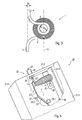
- the amplifier 20 is an amplifier 20 as the circuit to be protected shown as a perspective section in which the Surge protection device according to the invention arranged is.
- the amplifier 20 has a housing with Side walls 21.1 and 21.3, and a housing cover 21.2, where all housing components with a ground potential are connected. There is still one inside the case Partition 21.4 shown with the inside of the housing is divided into individual chambers. The partition 21.4 is also connected to the ground potential.
- the amplifier 20 has one arranged in the side wall 21.3 High-frequency connection 22 on which, for example, a Antenna is connected.
- the coaxial high frequency connection 22 consists of a shield 24, which also, preferably over the side wall 21.3, with the Ground potential is connected.
- the actual signal line takes place via a contact 23, which is inside the Housing is carried out and carried out there Contact 23 'is designated.
- the coil 1 is with the tapered part 6, that is first end 3 of the coil 1, in the direction of the performed Contact 23 'oriented.
- the first connector 4 is by means of a solder connection 30 with the carried out Contact 23 'conductively connected.
- the solder joint 30 is to be arranged so that the length of the performed Contact 23 'is as small as possible.
- Another one Solder connection 29 is the second connector 5 with a Ground potential 28 connected.
- the ground potential 28 can, for example the metallic back of a circuit board 25, on which the components of the amplifier circuit are arranged. Examples are components 26.1 and 26.2 in partial elevation shown. On the circuit board 25 are in itself known high-frequency conductor 27 is formed.
- the ground potential 28 forms with the partition 21.4 and the rest also connected to the ground potential 28 Components of a conductive unit.
- the ground potential 28 and the housing cover 21.2 parallel surfaces, both of which are at ground potential.
- the assembly plane 10 becomes symmetrical between the surface of the housing cover 21.2 and the area of the ground potential 28 arranged.
- the distance is the Coil axis 2 of the side wall 21.3 approximately as large as the distance of the mounting plane 10 from the ground potential 28 or the housing cover 21.2.
- the illustrated high-frequency connection 22 has one Nominal impedance of 50 ⁇ , the coil 1 should already be at the lowest operating frequency of z. B. 30 MHz of Amplifier 20 has a reactance of e.g. 500 ⁇ exhibit. With a mental breakdown of the coil 1 in several successive sections in the axial direction on the other hand, the first windings on the first End 3 of the coil 1 has a sufficiently high inductance achieves a reactance of for high frequencies Ensure 500 ⁇ . Because for the high frequencies only that so-called "hot end" of the coil is relevant, due to the small winding diameter in this Range, a sufficiently high resonance frequency of more than 400 MHz ensures that outside the useful bandwidth lies.
Landscapes
- Engineering & Computer Science (AREA)
- Power Engineering (AREA)
- Microelectronics & Electronic Packaging (AREA)
- Emergency Protection Circuit Devices (AREA)
Abstract
Description
- Fig. 1
- eine perspektivische Darstellung einer Spule mit einem sich verjüngenden Teil;
- Fig. 2
- eine Seitenansicht der Spule der erfindungsgemäßen Überspannungsschutzvorrichtung;
- Fig. 3
- eine stirnseitige Ansicht der Spule; und
- Fig. 4
- einen Ausschnitt eines Verstärkers mit einer darin angeordneten erfindungsgemäßen Überspannungsschutzvorrichtung in perspektivischer Darstellung.
Claims (11)
- Überspannungsschutzvorrichtung zum Schutz eines Hochfrequenzanschlusses (22) gegen Überspannung, die eine aus einem elektrisch leitfähigen Draht gewickelte Spule (1) umfaßt, wobei die Spule (1) in Richtung einer Spulenachse (2) zumindest einen sich in Richtung auf ein mit dem Hochfrequenzanschluß (22) verbundenes Endes (3) der Spule (1) verjüngenden Teil (6) aufweist.
- Überspannungsschutzvorrichtung nach Anspruch 1,
dadurch gekennzeichnet, daß die Spule einen zylindrischen Teil (7) aufweist. - Überspannungsschutzvorrichtung nach Anspruch 2,
dadurch gekennzeichnet, daß die Einhüllende des sich verjüngenden Teils (6) der Spule (1) eine Mantelfläche eines Kegelstumpfs bildet. - Überspannungsschutzvorrichtung nach Anspruch 2 oder 3,
dadurch gekennzeichnet, daß die Länge (l1) des sich verjüngenden Teils (6) der Spule (1) und die Länge (l2) des zylindrischen Teils (7) der Spule (1) jeweils in Richtung der Spulenachse (2) betrachtet sich um höchstens 1/3 der Gesamtlänge (1) unterscheiden. - Überspannungsschutzvorrichtung nach einem der Ansprüche 1 bis 4,
dadurch gekennzeichnet, daß das Verhältnis der kleinsten zu der größten von jeweils einer Wicklung umgebenen Fläche (¼D1 2π; ¼D2 2π) zwischen 2 und 10, bevorzugt zwischen 3 und 6, besonders bevorzugt zwischen 4 und 5, liegt. - Überspannungsschutzvorrichtung nach einem der Ansprüche 1 bis 5,
dadurch gekennzeichnet, daß die Spule (1) als Luftspule ausgebildet ist. - Überspannungsschutzvorrichtung nach einem der Ansprüche 1 bis 6,
dadurch gekennzeichnet, daß die Spule (1) aus einem Kupferlackdraht gewickelt ist. - Überspannungsschutzvorrichtung nach einem der Ansprüche 1 bis 7,
dadurch gekennzeichnet, daß die einzelnen Wicklungen der Spule (1) eng aneinander anliegend gewickelt sind. - Überspannungsschutzvorrichtung nach einem der Ansprüche 1 bis 8,
dadurch gekennzeichnet, daß der sich verjüngende Teil (6) über eine erste Kontaktstelle (30) mit einem Hochfrequenzleiter (23', 27) einer Schaltung (20) verbunden ist, und das entgegengesetzte Ende der Spule (1) über eine zweite Kontaktstelle (29) mit einem Massepotential (28) verbunden ist. - Überspannungsschutzvorrichtung nach einem der Ansprüche 1 bis 9,
dadurch gekennzeichnet, daß der sich verjüngende Teil (6) der Spule (1) direkt mit einem Kontakt (23) eines Hochfrequenzanschlusses (22) verbunden ist. - Überspannungsschutzvorrichtung nach einem der Ansprüche 1 bis 10,
dadurch gekennzeichnet, daß die Spulenachse (2) symmetrisch zwischen zumindest zwei mit einem Massepotential (28) verbundenen Flächen (21.1, 21.3, 28) angeordnet ist.
Applications Claiming Priority (2)
| Application Number | Priority Date | Filing Date | Title |
|---|---|---|---|
| DE10203850 | 2002-01-31 | ||
| DE2002103850 DE10203850A1 (de) | 2002-01-31 | 2002-01-31 | Überspannungsschutzvorrichtung |
Publications (2)
| Publication Number | Publication Date |
|---|---|
| EP1333454A1 true EP1333454A1 (de) | 2003-08-06 |
| EP1333454B1 EP1333454B1 (de) | 2010-01-13 |
Family
ID=7713477
Family Applications (1)
| Application Number | Title | Priority Date | Filing Date |
|---|---|---|---|
| EP20030001457 Expired - Lifetime EP1333454B1 (de) | 2002-01-31 | 2003-01-22 | Überspannungsschutzvorrichtung |
Country Status (2)
| Country | Link |
|---|---|
| EP (1) | EP1333454B1 (de) |
| DE (2) | DE10203850A1 (de) |
Cited By (1)
| Publication number | Priority date | Publication date | Assignee | Title |
|---|---|---|---|---|
| WO2013017366A2 (de) | 2011-08-04 | 2013-02-07 | Rohde & Schwarz Gmbh & Co. Kg | Überspannungsschutzvorrichtung mit spulenanordnung |
Citations (2)
| Publication number | Priority date | Publication date | Assignee | Title |
|---|---|---|---|---|
| EP0443173A1 (de) | 1989-12-26 | 1991-08-28 | Tektronix, Inc. | Durchstimmbarer monolithischer Breitbandinduktor |
| GB2293058A (en) | 1994-09-08 | 1996-03-13 | Gen Instrument Corp | Surge arrestor for RF devices |
Family Cites Families (4)
| Publication number | Priority date | Publication date | Assignee | Title |
|---|---|---|---|---|
| DE2409901C3 (de) * | 1974-03-01 | 1978-05-03 | Siemens Ag, 1000 Berlin Und 8000 Muenchen | Schaltungsanordnung zum Überlastungsschutz von spannungsempfindlichen Einrichtungen |
| DE3431537A1 (de) * | 1984-08-28 | 1986-03-13 | Gebhard 5880 Lüdenscheid Auth | Ueberspannungsfilter fuer antennensteckdosen |
| US5053910A (en) * | 1989-10-16 | 1991-10-01 | Perma Power Electronics, Inc. | Surge suppressor for coaxial transmission line |
| CH690150A5 (de) * | 1994-12-23 | 2000-05-15 | Huber+Suhner Ag | EMP-Filter. |
-
2002
- 2002-01-31 DE DE2002103850 patent/DE10203850A1/de not_active Withdrawn
-
2003
- 2003-01-22 EP EP20030001457 patent/EP1333454B1/de not_active Expired - Lifetime
- 2003-01-22 DE DE50312332T patent/DE50312332D1/de not_active Expired - Lifetime
Patent Citations (2)
| Publication number | Priority date | Publication date | Assignee | Title |
|---|---|---|---|---|
| EP0443173A1 (de) | 1989-12-26 | 1991-08-28 | Tektronix, Inc. | Durchstimmbarer monolithischer Breitbandinduktor |
| GB2293058A (en) | 1994-09-08 | 1996-03-13 | Gen Instrument Corp | Surge arrestor for RF devices |
Cited By (4)
| Publication number | Priority date | Publication date | Assignee | Title |
|---|---|---|---|---|
| WO2013017366A2 (de) | 2011-08-04 | 2013-02-07 | Rohde & Schwarz Gmbh & Co. Kg | Überspannungsschutzvorrichtung mit spulenanordnung |
| DE102011080411A1 (de) | 2011-08-04 | 2013-02-07 | Rohde & Schwarz Gmbh & Co. Kg | Überspannungsschutzvorrichtung mit Spulenanordnung |
| WO2013017366A3 (de) * | 2011-08-04 | 2013-04-04 | Rohde & Schwarz Gmbh & Co. Kg | Überspannungsschutzvorrichtung mit spulenanordnung |
| US9640970B2 (en) | 2011-08-04 | 2017-05-02 | Rohde & Schwarz Gmbh & Co. Kg | Over-voltage protection device having a coil assembly |
Also Published As
| Publication number | Publication date |
|---|---|
| DE10203850A1 (de) | 2003-08-14 |
| EP1333454B1 (de) | 2010-01-13 |
| DE50312332D1 (de) | 2010-03-04 |
Similar Documents
| Publication | Publication Date | Title |
|---|---|---|
| EP1516390B1 (de) | Störschutzfilter- und blitzstromableiter-einrichtung | |
| EP1329005B1 (de) | Störschutzfilter- und blitzstromableiter-einrichtung | |
| EP0978157B1 (de) | Breitband emp-ableiter | |
| CH696099A5 (de) | Überspannungsschutzvorrichtung. | |
| DE60107313T2 (de) | Überspannungsschutz für Breitband-Anpassungszweig | |
| CH675933A5 (en) | Triaxial electromagnetic pulse conductor - has inner conductor and two screening conductors with unit to maintain contact with overload conductor | |
| EP0855756A1 (de) | EMP-Ableiter | |
| DE10241431B4 (de) | Überspannungsschutzsystem für eine koaxiale Übertragungsleitung | |
| EP1333454B1 (de) | Überspannungsschutzvorrichtung | |
| DE102005053689A1 (de) | ESD-Schutzvorrichtung für ein elektrisches Bauelement | |
| EP1650843B1 (de) | Zündkerzenstecker | |
| DE3431537C2 (de) | ||
| CH660261A5 (en) | EMP suppressor in a coaxial conductor | |
| EP2740180B1 (de) | Überspannungsschutzvorrichtung mit spulenanordnung | |
| DE3212684A1 (de) | Kupplungsglied fuer elektrische koaxial-kabel oder -leitungen mit ueberspannungsschutz | |
| EP1665451B1 (de) | Richtkoppler in koaxialleitungstechnik | |
| DE10301982A1 (de) | Wellenleiter | |
| DE4222378C2 (de) | Überspannungsschutz-Zwischenstecker für Antennenanlagen | |
| DE102004056991B4 (de) | Bauelement zur Störwellenunterdrückung in Zündanlagen und Verfahren zu dessen Herstellung | |
| DE112021006782B4 (de) | Überspannungsschutzschaltung und überspannungsschutzverfahren | |
| DE9217814U1 (de) | Überspannungsschutzgerät | |
| EP1351345B1 (de) | Koaxialverbinder mit Überspannungsschutz | |
| CN115377710B (zh) | 一种具有短线路结构的平行堆叠型避雷器 | |
| DE4238328A1 (de) | Kapazitives Trennstück | |
| CH690150A5 (de) | EMP-Filter. |
Legal Events
| Date | Code | Title | Description |
|---|---|---|---|
| PUAI | Public reference made under article 153(3) epc to a published international application that has entered the european phase |
Free format text: ORIGINAL CODE: 0009012 |
|
| AK | Designated contracting states |
Designated state(s): AT BE BG CH CY CZ DE DK EE ES FI FR GB GR HU IE IT LI LU MC NL PT SE SI SK TR |
|
| AX | Request for extension of the european patent |
Extension state: AL LT LV MK RO |
|
| 17P | Request for examination filed |
Effective date: 20030709 |
|
| AKX | Designation fees paid |
Designated state(s): DE FR GB IT |
|
| 17Q | First examination report despatched |
Effective date: 20080819 |
|
| GRAP | Despatch of communication of intention to grant a patent |
Free format text: ORIGINAL CODE: EPIDOSNIGR1 |
|
| GRAS | Grant fee paid |
Free format text: ORIGINAL CODE: EPIDOSNIGR3 |
|
| GRAA | (expected) grant |
Free format text: ORIGINAL CODE: 0009210 |
|
| AK | Designated contracting states |
Kind code of ref document: B1 Designated state(s): DE FR GB IT |
|
| REG | Reference to a national code |
Ref country code: GB Ref legal event code: FG4D Free format text: NOT ENGLISH |
|
| REF | Corresponds to: |
Ref document number: 50312332 Country of ref document: DE Date of ref document: 20100304 Kind code of ref document: P |
|
| PLBE | No opposition filed within time limit |
Free format text: ORIGINAL CODE: 0009261 |
|
| STAA | Information on the status of an ep patent application or granted ep patent |
Free format text: STATUS: NO OPPOSITION FILED WITHIN TIME LIMIT |
|
| 26N | No opposition filed |
Effective date: 20101014 |
|
| REG | Reference to a national code |
Ref country code: FR Ref legal event code: PLFP Year of fee payment: 14 |
|
| REG | Reference to a national code |
Ref country code: FR Ref legal event code: PLFP Year of fee payment: 15 |
|
| REG | Reference to a national code |
Ref country code: FR Ref legal event code: PLFP Year of fee payment: 16 |
|
| PGFP | Annual fee paid to national office [announced via postgrant information from national office to epo] |
Ref country code: GB Payment date: 20220125 Year of fee payment: 20 Ref country code: DE Payment date: 20220120 Year of fee payment: 20 |
|
| PGFP | Annual fee paid to national office [announced via postgrant information from national office to epo] |
Ref country code: IT Payment date: 20220124 Year of fee payment: 20 Ref country code: FR Payment date: 20220120 Year of fee payment: 20 |
|
| REG | Reference to a national code |
Ref country code: DE Ref legal event code: R071 Ref document number: 50312332 Country of ref document: DE |
|
| REG | Reference to a national code |
Ref country code: GB Ref legal event code: PE20 Expiry date: 20230121 |
|
| PG25 | Lapsed in a contracting state [announced via postgrant information from national office to epo] |
Ref country code: GB Free format text: LAPSE BECAUSE OF EXPIRATION OF PROTECTION Effective date: 20230121 |