EP1333309A2 - Dispersionskompensator mit flacher Durchlasskurve - Google Patents
Dispersionskompensator mit flacher Durchlasskurve Download PDFInfo
- Publication number
- EP1333309A2 EP1333309A2 EP03000628A EP03000628A EP1333309A2 EP 1333309 A2 EP1333309 A2 EP 1333309A2 EP 03000628 A EP03000628 A EP 03000628A EP 03000628 A EP03000628 A EP 03000628A EP 1333309 A2 EP1333309 A2 EP 1333309A2
- Authority
- EP
- European Patent Office
- Prior art keywords
- dispersion compensator
- mirror
- wavelength
- distribution
- light
- Prior art date
- Legal status (The legal status is an assumption and is not a legal conclusion. Google has not performed a legal analysis and makes no representation as to the accuracy of the status listed.)
- Granted
Links
- 239000006185 dispersion Substances 0.000 title claims abstract description 79
- 230000005540 biological transmission Effects 0.000 title claims abstract description 39
- 238000003780 insertion Methods 0.000 claims abstract description 45
- 230000037431 insertion Effects 0.000 claims abstract description 45
- 238000009826 distribution Methods 0.000 claims description 60
- 230000003287 optical effect Effects 0.000 claims description 33
- BJQHLKABXJIVAM-UHFFFAOYSA-N bis(2-ethylhexyl) phthalate Chemical compound CCCCC(CC)COC(=O)C1=CC=CC=C1C(=O)OCC(CC)CCCC BJQHLKABXJIVAM-UHFFFAOYSA-N 0.000 claims description 14
- 238000004891 communication Methods 0.000 claims description 11
- 239000000758 substrate Substances 0.000 claims description 11
- 238000005457 optimization Methods 0.000 claims description 8
- 239000000470 constituent Substances 0.000 claims description 5
- 239000002245 particle Substances 0.000 claims description 5
- 230000002093 peripheral effect Effects 0.000 claims description 5
- 150000001875 compounds Chemical class 0.000 claims description 4
- 239000000835 fiber Substances 0.000 abstract description 7
- 229910052751 metal Inorganic materials 0.000 description 33
- 239000002184 metal Substances 0.000 description 33
- 238000000034 method Methods 0.000 description 16
- 238000004519 manufacturing process Methods 0.000 description 12
- 238000002834 transmittance Methods 0.000 description 12
- VYPSYNLAJGMNEJ-UHFFFAOYSA-N Silicium dioxide Chemical compound O=[Si]=O VYPSYNLAJGMNEJ-UHFFFAOYSA-N 0.000 description 6
- 230000015556 catabolic process Effects 0.000 description 4
- 238000006731 degradation reaction Methods 0.000 description 4
- 239000011521 glass Substances 0.000 description 4
- 229910052804 chromium Inorganic materials 0.000 description 3
- 229910052681 coesite Inorganic materials 0.000 description 3
- 229910052906 cristobalite Inorganic materials 0.000 description 3
- 239000000377 silicon dioxide Substances 0.000 description 3
- 229910052682 stishovite Inorganic materials 0.000 description 3
- 229910052905 tridymite Inorganic materials 0.000 description 3
- 150000002500 ions Chemical class 0.000 description 2
- 230000031700 light absorption Effects 0.000 description 2
- 229910052759 nickel Inorganic materials 0.000 description 2
- 229910052723 transition metal Inorganic materials 0.000 description 2
- 239000012780 transparent material Substances 0.000 description 2
- 229910052691 Erbium Inorganic materials 0.000 description 1
- 229910052779 Neodymium Inorganic materials 0.000 description 1
- 239000011358 absorbing material Substances 0.000 description 1
- 238000010521 absorption reaction Methods 0.000 description 1
- 229910052782 aluminium Inorganic materials 0.000 description 1
- PNEYBMLMFCGWSK-UHFFFAOYSA-N aluminium oxide Inorganic materials [O-2].[O-2].[O-2].[Al+3].[Al+3] PNEYBMLMFCGWSK-UHFFFAOYSA-N 0.000 description 1
- 230000008033 biological extinction Effects 0.000 description 1
- 238000005094 computer simulation Methods 0.000 description 1
- 229910052802 copper Inorganic materials 0.000 description 1
- 229910052593 corundum Inorganic materials 0.000 description 1
- 230000008878 coupling Effects 0.000 description 1
- 238000010168 coupling process Methods 0.000 description 1
- 238000005859 coupling reaction Methods 0.000 description 1
- 230000007423 decrease Effects 0.000 description 1
- 230000000694 effects Effects 0.000 description 1
- 238000005516 engineering process Methods 0.000 description 1
- 239000010419 fine particle Substances 0.000 description 1
- 229910052742 iron Inorganic materials 0.000 description 1
- MRELNEQAGSRDBK-UHFFFAOYSA-N lanthanum oxide Inorganic materials [O-2].[O-2].[O-2].[La+3].[La+3] MRELNEQAGSRDBK-UHFFFAOYSA-N 0.000 description 1
- 229910001635 magnesium fluoride Inorganic materials 0.000 description 1
- 229910052748 manganese Inorganic materials 0.000 description 1
- 239000000463 material Substances 0.000 description 1
- 150000002739 metals Chemical class 0.000 description 1
- KTUFCUMIWABKDW-UHFFFAOYSA-N oxo(oxolanthaniooxy)lanthanum Chemical compound O=[La]O[La]=O KTUFCUMIWABKDW-UHFFFAOYSA-N 0.000 description 1
- 230000000644 propagated effect Effects 0.000 description 1
- 230000001902 propagating effect Effects 0.000 description 1
- 229910052761 rare earth metal Inorganic materials 0.000 description 1
- 229910052709 silver Inorganic materials 0.000 description 1
- 238000003892 spreading Methods 0.000 description 1
- 238000004544 sputter deposition Methods 0.000 description 1
- 150000003624 transition metals Chemical class 0.000 description 1
- 229910052720 vanadium Inorganic materials 0.000 description 1
- 238000007740 vapor deposition Methods 0.000 description 1
- 229910001845 yogo sapphire Inorganic materials 0.000 description 1
Images


Classifications
-
- G—PHYSICS
- G02—OPTICS
- G02B—OPTICAL ELEMENTS, SYSTEMS OR APPARATUS
- G02B6/00—Light guides; Structural details of arrangements comprising light guides and other optical elements, e.g. couplings
- G02B6/24—Coupling light guides
- G02B6/26—Optical coupling means
- G02B6/28—Optical coupling means having data bus means, i.e. plural waveguides interconnected and providing an inherently bidirectional system by mixing and splitting signals
- G02B6/293—Optical coupling means having data bus means, i.e. plural waveguides interconnected and providing an inherently bidirectional system by mixing and splitting signals with wavelength selective means
- G02B6/29346—Optical coupling means having data bus means, i.e. plural waveguides interconnected and providing an inherently bidirectional system by mixing and splitting signals with wavelength selective means operating by wave or beam interference
- G02B6/29358—Multiple beam interferometer external to a light guide, e.g. Fabry-Pérot, etalon, VIPA plate, OTDL plate, continuous interferometer, parallel plate resonator
-
- G—PHYSICS
- G02—OPTICS
- G02B—OPTICAL ELEMENTS, SYSTEMS OR APPARATUS
- G02B6/00—Light guides; Structural details of arrangements comprising light guides and other optical elements, e.g. couplings
- G02B6/24—Coupling light guides
- G02B6/26—Optical coupling means
- G02B6/28—Optical coupling means having data bus means, i.e. plural waveguides interconnected and providing an inherently bidirectional system by mixing and splitting signals
- G02B6/293—Optical coupling means having data bus means, i.e. plural waveguides interconnected and providing an inherently bidirectional system by mixing and splitting signals with wavelength selective means
- G02B6/29379—Optical coupling means having data bus means, i.e. plural waveguides interconnected and providing an inherently bidirectional system by mixing and splitting signals with wavelength selective means characterised by the function or use of the complete device
- G02B6/29392—Controlling dispersion
- G02B6/29394—Compensating wavelength dispersion
Definitions
- the present invention relates to a dispersion compensator of optical communications technology.
- a wavelength dispersion compensator which compensates for wavelength dispersion in an optical communication by using an optical element called a VIPA element, has been studied and developed.
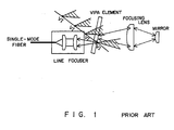
- Fig. 1 shows the basic configuration of a wavelength dispersion compensator using a VIPA element.
- the VIPA element is configured by forming reflection planes on both sides of a parallel flat plate of glass, etc., and by arranging an irradiation window for inputting light to part of a reflection plane.
- one of reflectances of the reflected planes is approximately 100%, whereas the other is equal to or lower than 100%, typically, 95% or so.
- An optical signal used in an optical communication is input from a single-mode fiber to a line focuser.
- the line focuser the light output and spread from the single-mode fiber is once made into parallel light beams, and then collected into linear light with a cylindrical lens, etc.
- the light collected by the line focuser passes through the irradiation window of the VIPA element, and is collected on the inside of the VIPA element.
- This light beam is collected by a focusing lens, and reflected on a mirror.
- the light beam then passes through the focusing lens and the VIPA element, and is coupled by the single-mode fiber that forms the line focuser.
- attention is paid to one light beam.
- the light beam is reflected on the mirror, passes through the focusing lens, and again enters the VIPA element, a difference exists between the optical distances of virtual image VIs as is known from Fig. 1 if the virtual image VI from which the light beam is output is made to differ from the virtual image VI to which the light beam that again enters the VIPA element is input, depending on a wavelength of a light beam. Therefore, an optical distance traveled by a light beam differs depending on a wavelength.
- a dispersion compensator implemented by using this phenomenon is a wavelength dispersion compensator using a VIPA element.
- a level of an optical signal differs depending on a wavelength and is output if such a wavelength dispersion compensator is used for an optical signal like wavelength-multiplexed light.
- an insertion loss transmission characteristic of the VIPA element is not flat.
- optimization such as flattening of an insertion loss wavelength characteristic of a transmission channel band of an optical element, and by extension, flattening, etc. of an insertion loss of a transmission channel bandwidth of the periphery of the dispersion compensator, its system, and entire network must be performed.
- An object of the present invention is to provide a dispersion compensator that can flatten or can make into a desired characteristic the transmission band of light.
- a dispersion compensator comprises: a wavelength dispersion compensating unit composed of an angular dispersing unit outputting input light in a different direction depending on each wavelength, and a mirror unit reflecting the light output from the angular dispersing unit, and again inputting the light to the angular dispersing unit; and an optimizing unit optimizing an insertion loss wavelength characteristic of the wavelength dispersion compensating unit.
- the insertion loss wavelength characteristic of the dispersion compensator into a desired characteristic, and especially, to easily flatten an insertion loss wavelength characteristic having steep wavelength dependency. It is also possible to make the insertion loss wavelength characteristic of not only the dispersion compensator but also peripheral devices including the dispersion compensator, an optical communications system or network including the dispersion compensator into a desired characteristic with the optimizing unit.
- the insertion loss wavelength characteristic of the dispersion compensator, its peripheral devices, optical communications system or network, etc. steeply changes over a bandwidth where an optical signal is propagated, it can be corrected to a characteristic suitable for propagating the optical signal.
- Preferred embodiments according to the present invention provide the following configurations and their operations.
- a space filter whose transmittance distributes two-dimensionally is inserted between a VIPA plate (or a VIPA element) and a focusing lens, or between the focusing lens and a mirror. Or, a two-dimensional reflectance is made to distribute on the surface of the mirror. Furthermore, a periodical characteristic filter whose transmission loss characteristic has periodicity, such as an etalon filter, etc. is inserted in a line focuser.
- the insertion loss characteristic of the dispersion compensator and the transmission loss characteristic of the space filter or the periodical characteristic filter are superimposed, so that an optimized insertion loss wavelength characteristic of a transmission channel band can be obtained.
- the mirror reflectance characteristic and the original insertion loss characteristic of the wavelength dispersion compensation are superimposed, so that an optimized insertion loss wavelength characteristic of a transmission channel band can be obtained.
- an insertion loss wavelength characteristic of a transmission channel band which is optimized by superimposing the insertion loss characteristic of the dispersion compensator on the transmission loss characteristic of the etalon filter, can be obtained.
- optimizations such as flattening, etc. of the insertion loss wavelength characteristic of a transmission channel band of the periphery of the wavelength dispersion compensator, its system and entire network can be performed.
- Control of the space filter or the mirror reflectance is performed as follows.
- a mirror having a two-dimensional reflectance distribution is formed by imparting a two-dimensional thickness distribution to the metal reflection film.
- the shape of the surface of the mirror differs from a designed shape, leading to a degradation of optical characteristics such as dispersion, a group delay, etc. in some cases . Therefore, the shape of a mirror substrate is formed by expecting the thickness distribution of the metal film, and a desired mirror shape is obtained, so that the degradation of the optical characteristics can be prevented.
- the shape of the surface of the mirror differs from a designed shape, and optical characteristics such as wavelength dispersion, a group delay, etc. are sometimes degraded.
- the metal reflection film having the two-dimensional thickness distribution is formed as two layers (or more), and a two-dimensional thickness distribution is imparted to the first layer metal reflection film on the input side of light, so that a reflectance distribution is made to occur.
- a thickness distribution reverse to the first layer metal film is imparted to the second layer metal film or a dielectric film on the input side of light, so that the shape of the surface of the mirror substrate can be maintained as a designed value unchanged, and the degradation of the optical characteristics can be prevented.
- the metal reflection film can be formed with a film forming technique such as sputtering, vapor deposition, etc.
- a thickness distribution is generated by changing the probability that the constituent particles of the film adhere to the substrate with the use of a mask preventing the proceeding of constituent particles of a film.
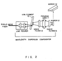
- Fig. 2 exemplifies a first configuration using the space filter according to the preferred embodiment of the present invention.
- a space filter 13 is arranged between a VIPA element 10, which is explained with reference to Fig. 1, and a focusing lens 11, or between the focusing lens 11 and a mirror 12 of an angular dispersion compensator.
- the mirror 12 is a mirror whose curved surface continually changes in a way such that one end has a concave surface, the central part has a plain surface, and the other end has a convex surface.
- the curved surface of the mirror 12 is continually changed in the direction orthogonal to the direction of the paper (the direction where angular dispersion is given by the VIPA), so that a wavelength dispersion amount can be adjusted to an arbitrary value.
- the space filter 13 is moved in correspondence with the mirror 12.
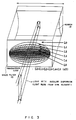
- Fig. 3 shows the relationship between the transmission loss distribution of the space filter and the mirror.
- the transmission loss gradually increases from L0 to L5.
- This figure assumes the case where the insertion loss characteristic of the VIPA element or the entire wavelength dispersion compensator is small in the proximity of the center of the transmission band, and sharply increases as apart from the center.
- the loss is the largest in the L5 region in the proximity of the center of the space filter, which corresponds to the proximity of the center of the transmission band, and gradually decreases toward the periphery of the space filter.
- the filter is configured so that its transmission loss distribution converges in the form of an ellipse in the left and the right direction of the sheet of paper.
- the loss distribution to be given to a light beam that passes through the space filter differs for the light (a light beam from the VIPA element) which is given an angular dispersion according to a position where the mirror 12 moves (the mirror 12 moves according to the dispersion amount in the direction indicated by an arrow).
- the ends of the mirror 12 in the move direction are shaped like convex and concave so that a loss distribution of the space filter 13 is narrow in the direction of the angular dispersion, and the loss distribution of the space filter 13 where the shape of the mirror 12 is flat, largely distributes outside in the direction of the angular dispersion of a light beam. Therefore, the space filter 13 has a loss distribution in the form of an ellipse in the move direction of the mirror 12 in correspondence with the curved surface of the mirror 12.
- the loss distribution can be arbitrarily configured in correspondence with the shape of the curved surface of the mirror.
- Fig. 4 exemplifies a second configuration according to a preferred embodiment of the present invention.
- the reflectance of the surface of a mirror 12a is changed two-dimensionally. Namely, a loss is made large on the surface where strong light is irradiated, and made small on the surface where weak light is irradiated.
- the mirror 12a whose reflection plane continually changes from concave to convex, is moved in the direction perpendicular to the sheet of paper in a similar manner as in Fig. 2.
- Fig. 5 shows the reflectance distribution of a mirror having a two-dimensional reflectance distribution.
- the reflectance is configured to gradually increase from R5 to R0.
- an assumed loss insertion characteristic of the VIPA element or the wavelength dispersion compensator is similar to that in the case shown in Fig. 4. Accordingly, the reflectance is the smallest in the R5 region that is the proximity of the center of the transmission band where the intensity of input light is the highest, and the largest in the RO region where the intensity of input light is the lowest.
- a distribution of this reflectance is configured in correspondence with the shape of the curved surface of the reflection plane similar to the distribution of the transmission loss of the space filter 13 shown in Fig. 2.
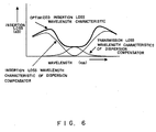
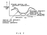
- Figs. 6 and 7 explain the effects of the configuration examples of the preferred embodiments shown in Figs. 2 to 5.
- Fig. 6 shows an optimized insertion loss wavelength characteristic when the space filter is used.
- the insertion loss wavelength characteristic of the wavelength dispersion compensator is optimized by being superimposed on the transmission loss wavelength characteristic of the space filter, so that the optimized insertion loss wavelength characteristic is implemented.
- the optimization is not limited to the widening of a flattened transmission channel band, and indicates the equalization of the transmission channel band of the periphery of the wavelength dispersion compensator (peripheral devices including the wavelength dispersion compensator), and an optical communications system and an entire optical communications network, which include the wavelength dispersion compensator, and also indicates the optimization of the insertion loss wavelength characteristic by adjusting the transmittance of the space filter, for the insertion loss wavelength characteristic of the wavelength dispersion compensator.
- Fig. 7 shows an optimized insertion loss wavelength characteristic in the case where the reflectance of the mirror is changed two-dimensionally.
- the insertion loss wavelength characteristic of the wavelength dispersion compensator is optimized by being superimposed on the reflectance wavelength characteristic of the mirror having a two-dimensional reflectance distribution, so that the optimized insertion loss wavelength characteristic is implemented.
- the optimization is not limited to the widening of a flattened transmission channel band, and indicates the equalization of the transmission channel band of the periphery of the wavelength dispersion compensator (peripheral devices including the wavelength dispersion compensator), and an optical communication system and an entire optical communications network, which include the wavelength dispersion compensator, and also indicates the optimization of the insertion loss characteristic by adjusting the transmittance of a space filter, for the insertion loss wavelength characteristic of the wavelength dispersion compensator.
- the insertion loss wavelength characteristic of the wavelength dispersion compensator can be flattened with the space filter having a suitable transmission loss characteristic or the mirror having a suitable reflectance.
- the insertion loss wavelength characteristic of the wavelength dispersion compensator can be controlled in a variety of ways by changing the transmission loss of the space filter or the reflectance of the mirror, and the object to vary the insertion loss wavelength characteristic is not necessarily limited to the flattening of the transmission band.
- a device having the transmission loss wavelength characteristic of the space filter that is shown in Fig. 5 and is repeated periodically in a wavelength dimension which is disclosed by a known technique such as the U.S. Patent No. 5,809,190, etc., is connected in series, so that the optimized insertion loss wavelength characteristic shown in Fig. 5 can be implemented.
- Fig. 8 explains a space filter having a two-dimensional transmittance distribution.
- the space filter having the two-dimensional transmittance distribution shown in Fig. 3 can be obtained by spreading, for example, Co being a transition metal as an element which absorbs light within a plate composed of a transparent material such as glass, and by making its concentration distribute two-dimensionally.
- a transparent material such as plastic, etc.
- Cr, Cu, Fe, Ni, Mn, V, etc. which are transition metal elements other than Co, or their ions, a compound such as an oxide, an organic metal, etc., Al being a typical metal element, and Er, Nd, etc. being rare-earth elements may be available.
- space filter having the two-dimensional transmittance distribution is arranged between the VIPA element and the mirror within the dispersion compensator, whereby the optimized insertion loss wavelength characteristic shown in Fig. 6 can be implemented. Additionally, at this time, a light beam passes through the space filter twice. Therefore, its transmission characteristic must be designed to become the characteristic shown in Fig. 6 after passing through the space filter twice. It is desirable from the principle of a VIPA dispersion compensator to arrange the space filter as close as possible to the mirror between the focusing lens 11 and the mirror 12 in Fig. 2. This is because a position of the space filter through which a light beam passes significantly varies depending on a wavelength
- This preferred embodiment refers to the example where the material absorbing light is made to two-dimensionally distribute on a transparent substrate of glass, etc.
- a film having an extinction distribution which is generated by making the concentration of such a light absorbing material distribute two-dimensionally, or a film having an absorption distribution, which is generated by making the thickness of a light absorbing film distribute two-dimensionally, may be available.
- Fig. 9 exemplifies another configuration using the etalon filter according to the preferred embodiment of the present invention.
- the optimized insertion loss wavelength characteristic shown in Fig. 6 can be implemented also by inserting the etalon filter having a periodical transmission characteristic in between a collimate lens 16 and a cylindrical lens 17 within a line focuser of a wavelength dispersion compensator, between which a collimated light beam travels.
- the light beam passes through the etalon filter twice from when it enters from a single-mode fiber till when it again enters the single-mode fiber after being reflected off a mirror. Therefore, its transmission characteristic must be designed to become the characteristic shown in Fig. 6 after passing through the etalon filter twice.
- the insertion loss wavelength characteristic of the dispersion compensator which is shown in Fig. 6, is flattened, an adjustment is made in such a way that a low portion of the transmittance of the etalon filter is positioned in a portion corresponding to a small loss of the insertion loss wavelength characteristic of the dispersion compensator.
- the etalon filter is not moved in correspondence with the move of the mirror 12 as in the previous preferred embodiment, but fixed.
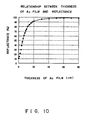
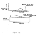
- Figs. 10 to 14 explain a method manufacturing a mirror whose reflectance exhibits a two-dimensional distribution.
- a metal used as a metal reflection film of the mirror for example, Au is available.
- the thickness of an Au film is equal to or thinner than 80 nm as shown in Fig. 10
- the thickness of the Au film is adjusted within the range of equal to or thinner than 80 nm as shown in Fig. 11, a mirror whose reflectance distributes spatially is obtained.
- a Au metal reflection film whose central thickness is thin is arranged on a mirror substrate. If the thickness of the Au metal film varies within the range of 80 nm as shown in an upper stage of Fig. 11, it exerts an influence on the reflectance of the mirror.
- a reflection loss is large in the proximity of the center of the Au film, and accordingly, its reflectance can be set to a small value. Furthermore, the thickness of the Au film is made to two-dimensionally distribute as shown in Fig. 12, whereby it becomes possible make the reflectance two-dimensionally distribute as shown in Fib. 5.
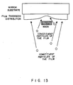
- the film thickness distribution shown in Fig. 11 can be generated by changing the probability that the constituent particles of a film (Au fine particles, atoms, etc.) adhere to the substrate, for example, with the use of a mask which prevents the proceeding of constituent particles of a film as shown in Fig. 13. Furthermore, a two-dimensional film thickness distribution shown in Fig. 12 can be imparted by using a two-dimensional mask shown in Fig. 14.
- This preferred embodiment refers to the case where Au is used.
- other metals such as Ag, Al, Cr, etc. may be available, and a used metal is not limited particularly.
- mirror having the two-dimensional reflectance is used for the wavelength dispersion compensator as shown in Fig. 4, whereby the optimized insertion loss wavelength characteristic shown in Fig. 7 can be implemented.
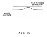
- Fig. 15 explains another method manufacturing a mirror whose reflectance distributes two-dimensionally.
- the shape of the mirror substantially becomes the surface of the metal film as shown in Fig. 11. Therefore, it can possibly differ from the original shape of the surface of the mirror substrate due to the thickness distribution of the metal film.
- optical characteristics such as wavelength dispersion, a group delay, etc., which the wavelength dispersion compensator gives to light, are determined depending on the shape of the mirror. Therefore, the optical characteristics such as wavelength dispersion, a group delay, etc. are sometimes degraded because the shape of the mirror differs from the original shape.
- the shape of the mirror is formed by taking into account a film thickness distribution as shown in Fig. 15, so that a desired mirror shape can be obtained, and the optical characteristics can be prevented from being degraded.
- Figs. 16 and 17 explain a further method manufacturing a mirror whose reflectance distributes two-dimensionally.
- the manufacturing method shown in Fig. 15 can prevent the optical characteristics from being degraded due to a film thickness distribution. However, this method makes the process of a mirror complex.
- a metal reflection film having a two-dimensional thickness distribution is configured as two layers as shown in Fig. 16, and a two-dimensional thickness distribution is imparted to the first layer metal reflection film on the input side of light, so that a reflectance distribution is made to occur.
- a thickness distribution reverse to that of the first layer metal film may be imparted to the second layer metal film on the input side of light so as to make the thickness of the entire reflection film uniform.
- reflection from the surface of the Cr film cannot be ignored, but a positive correlation exists between the thickness of the Au film and the reflectance as shown in Fig. 17. Therefore, such a mirror can be designed.
- a protection film of a dielectric film of SiO 2 , etc. is coated on the metal reflection film, or Cr, Ni, etc. may be undercoated on the lower side of the metal reflection film, and the number of layers may be equal to or larger than 2.
- the characteristics of an ultrahigh-speed, an ultralarge-capacity, and an ultralong-haul optical wavelength multiplexing transmitting device can be improved.
Applications Claiming Priority (2)
| Application Number | Priority Date | Filing Date | Title |
|---|---|---|---|
| JP2002006824A JP4030763B2 (ja) | 2002-01-16 | 2002-01-16 | 透過帯域平坦化された分散補償器 |
| JP2002006824 | 2002-01-16 |
Publications (3)
| Publication Number | Publication Date |
|---|---|
| EP1333309A2 true EP1333309A2 (de) | 2003-08-06 |
| EP1333309A3 EP1333309A3 (de) | 2004-12-08 |
| EP1333309B1 EP1333309B1 (de) | 2006-04-26 |
Family
ID=19191275
Family Applications (1)
| Application Number | Title | Priority Date | Filing Date |
|---|---|---|---|
| EP03000628A Expired - Fee Related EP1333309B1 (de) | 2002-01-16 | 2003-01-15 | Dispersionskompensator mit flacher Durchlasskurve |
Country Status (4)
| Country | Link |
|---|---|
| US (1) | US6909537B2 (de) |
| EP (1) | EP1333309B1 (de) |
| JP (1) | JP4030763B2 (de) |
| DE (1) | DE60304750T2 (de) |
Families Citing this family (5)
| Publication number | Priority date | Publication date | Assignee | Title |
|---|---|---|---|---|
| US6714705B1 (en) * | 2002-05-07 | 2004-03-30 | Avanex Corporation | Tunable chromatic dispersion and dispersion slope compensator utilizing a virtually imaged phased array and a rotating grating |
| JP4518825B2 (ja) * | 2004-03-31 | 2010-08-04 | 富士通株式会社 | 可変波長分散補償器 |
| JP2006243500A (ja) | 2005-03-04 | 2006-09-14 | Fujitsu Ltd | 波長分散補償器 |
| JP4613814B2 (ja) * | 2005-12-26 | 2011-01-19 | 日立金属株式会社 | 可変分散補償器 |
| CN111712980B (zh) * | 2018-02-14 | 2023-06-06 | 古河电气工业株式会社 | 光模块、其波长控制方法以及其校准方法 |
Citations (5)
| Publication number | Priority date | Publication date | Assignee | Title |
|---|---|---|---|---|
| WO1996031961A1 (en) * | 1995-04-05 | 1996-10-10 | Jds Fitel Inc. | Chromatic dispersion compensation device |
| US6028706A (en) * | 1995-07-26 | 2000-02-22 | Fujitsu Limited | Virtually imaged phased array (VIPA) having a varying reflectivity surface to improve beam profile |
| US6332689B1 (en) * | 1999-12-14 | 2001-12-25 | Fujitsu Limited | Optical apparatus which uses a virtually imaged phased array to produce chromatic dispersion |
| WO2002023234A1 (fr) * | 2000-09-14 | 2002-03-21 | Oyokoden Lab Co., Ltd. | Dispositif de compensation de la dispersion optique, dispositif composite de compensation de la dispersion optique comportant ledit dispositif et procede de compensation de la dispersion optique a l'aide de ce dispositif |
| US20030128431A1 (en) * | 2002-01-09 | 2003-07-10 | Nobuaki Mitamura | Optical device |
Family Cites Families (8)
| Publication number | Priority date | Publication date | Assignee | Title |
|---|---|---|---|---|
| JP3464081B2 (ja) * | 1995-07-26 | 2003-11-05 | 富士通株式会社 | 波長分波器 |
| US5969865A (en) * | 1995-07-26 | 1999-10-19 | Fujitsu Limited | Optical apparatus which uses a virtually imaged phased array to produce chromatic dispersion |
| US5930045A (en) * | 1995-07-26 | 1999-07-27 | Fujitsu, Ltd. | Optical apparatus which uses a virtually imaged phased array to produce chromatic dispersion |
| US5973838A (en) * | 1995-07-26 | 1999-10-26 | Fujitsu Limited | Apparatus which includes a virtually imaged phased array (VIPA) in combination with a wavelength splitter to demultiplex wavelength division multiplexed (WDM) light |
| US6556320B1 (en) * | 2000-05-19 | 2003-04-29 | Avanex Corporation | Tunable chromatic dispersion, dispersion slope, and polarization mode dispersion compensator utilizing a virtually imaged phased array |
| US6744991B1 (en) * | 2000-05-19 | 2004-06-01 | Avanex Corporation | Tunable chromatic dispersion and polarization mode dispersion compensator utilizing a virtually imaged phased array |
| US6668115B2 (en) * | 2000-12-22 | 2003-12-23 | Avanex Corporation | Method, apparatus, and system for compensation of amplifier gain slope and chromatic dispersion utilizing a virtually imaged phased array |
| US6714705B1 (en) * | 2002-05-07 | 2004-03-30 | Avanex Corporation | Tunable chromatic dispersion and dispersion slope compensator utilizing a virtually imaged phased array and a rotating grating |
-
2002
- 2002-01-16 JP JP2002006824A patent/JP4030763B2/ja not_active Expired - Fee Related
-
2003
- 2003-01-13 US US10/340,842 patent/US6909537B2/en not_active Expired - Fee Related
- 2003-01-15 DE DE60304750T patent/DE60304750T2/de not_active Expired - Fee Related
- 2003-01-15 EP EP03000628A patent/EP1333309B1/de not_active Expired - Fee Related
Patent Citations (6)
| Publication number | Priority date | Publication date | Assignee | Title |
|---|---|---|---|---|
| WO1996031961A1 (en) * | 1995-04-05 | 1996-10-10 | Jds Fitel Inc. | Chromatic dispersion compensation device |
| US6028706A (en) * | 1995-07-26 | 2000-02-22 | Fujitsu Limited | Virtually imaged phased array (VIPA) having a varying reflectivity surface to improve beam profile |
| US6332689B1 (en) * | 1999-12-14 | 2001-12-25 | Fujitsu Limited | Optical apparatus which uses a virtually imaged phased array to produce chromatic dispersion |
| WO2002023234A1 (fr) * | 2000-09-14 | 2002-03-21 | Oyokoden Lab Co., Ltd. | Dispositif de compensation de la dispersion optique, dispositif composite de compensation de la dispersion optique comportant ledit dispositif et procede de compensation de la dispersion optique a l'aide de ce dispositif |
| US20020044738A1 (en) * | 2000-09-14 | 2002-04-18 | Jablonski Mark Kenneth | Completely thin-film based composite dispersion compensating structure and its method of use |
| US20030128431A1 (en) * | 2002-01-09 | 2003-07-10 | Nobuaki Mitamura | Optical device |
Also Published As
| Publication number | Publication date |
|---|---|
| EP1333309B1 (de) | 2006-04-26 |
| EP1333309A3 (de) | 2004-12-08 |
| JP2003207618A (ja) | 2003-07-25 |
| DE60304750T2 (de) | 2007-05-16 |
| DE60304750D1 (de) | 2006-06-01 |
| US6909537B2 (en) | 2005-06-21 |
| JP4030763B2 (ja) | 2008-01-09 |
| US20030147121A1 (en) | 2003-08-07 |
Similar Documents
| Publication | Publication Date | Title |
|---|---|---|
| US6296361B1 (en) | Optical apparatus which uses a virtually imaged phased array to produced chromatic dispersion | |
| US7193778B2 (en) | Optical apparatus which uses a virtually imaged phased array to produce chromatic dispersion | |
| US7075723B2 (en) | Optical apparatus which uses a virtually imaged phased array to produce chromatic dispersion | |
| CN100363769C (zh) | 光纤中的色散补偿 | |
| US6668115B2 (en) | Method, apparatus, and system for compensation of amplifier gain slope and chromatic dispersion utilizing a virtually imaged phased array | |
| CA2279712C (en) | An optical filter for use in or with an optical amplifier | |
| EP1703307B1 (de) | VIPA basierte Vorrichtung zur Kompensation der chromatischen Dispersion und des Dispersionsgradienten | |
| US6956700B1 (en) | Wavelength dispersion compensating apparatus | |
| US6909537B2 (en) | Dispersion compensator whose transmission band is flattened | |
| JP4095866B2 (ja) | 波長分散発生装置 | |
| US7161739B2 (en) | Optical system, optical device including the same, and optical device designing method | |
| JPH0651113A (ja) | 光バンドパスフィルタモジュール | |
| JP2006221075A (ja) | 可変分散補償器 |
Legal Events
| Date | Code | Title | Description |
|---|---|---|---|
| PUAI | Public reference made under article 153(3) epc to a published international application that has entered the european phase |
Free format text: ORIGINAL CODE: 0009012 |
|
| AK | Designated contracting states |
Designated state(s): AT BE BG CH CY CZ DE DK EE ES FI FR GB GR HU IE IT LI LU MC NL PT SE SI SK TR |
|
| AX | Request for extension of the european patent |
Extension state: AL LT LV MK RO |
|
| PUAL | Search report despatched |
Free format text: ORIGINAL CODE: 0009013 |
|
| AK | Designated contracting states |
Kind code of ref document: A3 Designated state(s): AT BE BG CH CY CZ DE DK EE ES FI FR GB GR HU IE IT LI LU MC NL PT SE SI SK TR |
|
| AX | Request for extension of the european patent |
Extension state: AL LT LV MK RO |
|
| 17P | Request for examination filed |
Effective date: 20050113 |
|
| 17Q | First examination report despatched |
Effective date: 20050429 |
|
| AKX | Designation fees paid |
Designated state(s): DE FR GB |
|
| GRAP | Despatch of communication of intention to grant a patent |
Free format text: ORIGINAL CODE: EPIDOSNIGR1 |
|
| GRAS | Grant fee paid |
Free format text: ORIGINAL CODE: EPIDOSNIGR3 |
|
| GRAA | (expected) grant |
Free format text: ORIGINAL CODE: 0009210 |
|
| AK | Designated contracting states |
Kind code of ref document: B1 Designated state(s): DE FR GB |
|
| REG | Reference to a national code |
Ref country code: GB Ref legal event code: FG4D |
|
| REF | Corresponds to: |
Ref document number: 60304750 Country of ref document: DE Date of ref document: 20060601 Kind code of ref document: P |
|
| ET | Fr: translation filed | ||
| PLBE | No opposition filed within time limit |
Free format text: ORIGINAL CODE: 0009261 |
|
| STAA | Information on the status of an ep patent application or granted ep patent |
Free format text: STATUS: NO OPPOSITION FILED WITHIN TIME LIMIT |
|
| 26N | No opposition filed |
Effective date: 20070129 |
|
| PGFP | Annual fee paid to national office [announced via postgrant information from national office to epo] |
Ref country code: DE Payment date: 20090108 Year of fee payment: 7 |
|
| PGFP | Annual fee paid to national office [announced via postgrant information from national office to epo] |
Ref country code: GB Payment date: 20090114 Year of fee payment: 7 |
|
| PGFP | Annual fee paid to national office [announced via postgrant information from national office to epo] |
Ref country code: FR Payment date: 20090113 Year of fee payment: 7 |
|
| GBPC | Gb: european patent ceased through non-payment of renewal fee |
Effective date: 20100115 |
|
| REG | Reference to a national code |
Ref country code: FR Ref legal event code: ST Effective date: 20100930 |
|
| PG25 | Lapsed in a contracting state [announced via postgrant information from national office to epo] |
Ref country code: FR Free format text: LAPSE BECAUSE OF NON-PAYMENT OF DUE FEES Effective date: 20100201 |
|
| PG25 | Lapsed in a contracting state [announced via postgrant information from national office to epo] |
Ref country code: DE Free format text: LAPSE BECAUSE OF NON-PAYMENT OF DUE FEES Effective date: 20100803 |
|
| PG25 | Lapsed in a contracting state [announced via postgrant information from national office to epo] |
Ref country code: GB Free format text: LAPSE BECAUSE OF NON-PAYMENT OF DUE FEES Effective date: 20100115 |