EP1332247B1 - Method and device for cutting single crystals, in addition to an adjusting device and a test method for determining a crystal orientation - Google Patents
Method and device for cutting single crystals, in addition to an adjusting device and a test method for determining a crystal orientation Download PDFInfo
- Publication number
- EP1332247B1 EP1332247B1 EP01960587A EP01960587A EP1332247B1 EP 1332247 B1 EP1332247 B1 EP 1332247B1 EP 01960587 A EP01960587 A EP 01960587A EP 01960587 A EP01960587 A EP 01960587A EP 1332247 B1 EP1332247 B1 EP 1332247B1
- Authority
- EP
- European Patent Office
- Prior art keywords
- single crystal
- cutting
- longitudinal axis
- angle
- cutting tool
- Prior art date
- Legal status (The legal status is an assumption and is not a legal conclusion. Google has not performed a legal analysis and makes no representation as to the accuracy of the status listed.)
- Expired - Lifetime
Links
Images


Classifications
-
- C—CHEMISTRY; METALLURGY
- C30—CRYSTAL GROWTH
- C30B—SINGLE-CRYSTAL GROWTH; UNIDIRECTIONAL SOLIDIFICATION OF EUTECTIC MATERIAL OR UNIDIRECTIONAL DEMIXING OF EUTECTOID MATERIAL; REFINING BY ZONE-MELTING OF MATERIAL; PRODUCTION OF A HOMOGENEOUS POLYCRYSTALLINE MATERIAL WITH DEFINED STRUCTURE; SINGLE CRYSTALS OR HOMOGENEOUS POLYCRYSTALLINE MATERIAL WITH DEFINED STRUCTURE; AFTER-TREATMENT OF SINGLE CRYSTALS OR A HOMOGENEOUS POLYCRYSTALLINE MATERIAL WITH DEFINED STRUCTURE; APPARATUS THEREFOR
- C30B33/00—After-treatment of single crystals or homogeneous polycrystalline material with defined structure
-
- B—PERFORMING OPERATIONS; TRANSPORTING
- B28—WORKING CEMENT, CLAY, OR STONE
- B28D—WORKING STONE OR STONE-LIKE MATERIALS
- B28D5/00—Fine working of gems, jewels, crystals, e.g. of semiconductor material; apparatus or devices therefor
-
- B—PERFORMING OPERATIONS; TRANSPORTING
- B28—WORKING CEMENT, CLAY, OR STONE
- B28D—WORKING STONE OR STONE-LIKE MATERIALS
- B28D5/00—Fine working of gems, jewels, crystals, e.g. of semiconductor material; apparatus or devices therefor
- B28D5/0058—Accessories specially adapted for use with machines for fine working of gems, jewels, crystals, e.g. of semiconductor material
- B28D5/0082—Accessories specially adapted for use with machines for fine working of gems, jewels, crystals, e.g. of semiconductor material for supporting, holding, feeding, conveying or discharging work
- B28D5/0088—Accessories specially adapted for use with machines for fine working of gems, jewels, crystals, e.g. of semiconductor material for supporting, holding, feeding, conveying or discharging work the supporting or holding device being angularly adjustable
-
- Y—GENERAL TAGGING OF NEW TECHNOLOGICAL DEVELOPMENTS; GENERAL TAGGING OF CROSS-SECTIONAL TECHNOLOGIES SPANNING OVER SEVERAL SECTIONS OF THE IPC; TECHNICAL SUBJECTS COVERED BY FORMER USPC CROSS-REFERENCE ART COLLECTIONS [XRACs] AND DIGESTS
- Y10—TECHNICAL SUBJECTS COVERED BY FORMER USPC
- Y10S—TECHNICAL SUBJECTS COVERED BY FORMER USPC CROSS-REFERENCE ART COLLECTIONS [XRACs] AND DIGESTS
- Y10S125/00—Stone working
- Y10S125/901—Stone working forming piezoelectric crystals
Definitions
- the invention relates to a method and a device for Separating single crystals, an adjusting device and a Test method for determining an orientation of a single crystal for such a procedure.
- the object is achieved by a method according to claim 1, a device according to claim 8, a device for adjusting according to claim 12 and a test method according to claim 16.
- the method and the device have the advantage that the Quality of the wafer is increased and that when separating higher Feed rates are possible. Thereby leaves especially for GaAs inner hole sawing also for wafers of 6 inches in diameter and possibly larger. By the Improved quality of the produced wafers can be otherwise usual Post-processing steps largely eliminated.
- an inventive Device according to a first embodiment
- the invention relates to a mecaniclochsägevorraum.
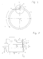
- a single crystal 1 of substantially cylindrical shape with a central longitudinal axis M is from a holder, not shown held.
- An inner hole cutting disc 2 which in known Way of a metal disk with a concentric hole at the boundary by applying diamond grains a cutting edge 3 is formed, is about an axis of rotation R rotatably supported relative to the single crystal, that the center longitudinal axis M of the single crystal and the axis of rotation R of the cutting disc parallel to each other.
- It is an unillustrated drive provided with the blade 2 at a defined speed about the rotation axis R in the direction shown in Fig. 1 A is rotatable.
- the single crystal 1 is via a drive a feed unit in the feed direction shown in Fig. 2 V in the direction of the cutting disc 2 so movable, that the cutting disc 2, the single crystal 1 completely in a plane perpendicular to its central longitudinal axis M cut through can. Furthermore, a drive is provided for moving of the single crystal 1 perpendicular to the cutting disk 2 or along the direction of its central longitudinal axis at a speed w.
- the single crystal is 1 not completely cylindrical, but has a flat Outside surface section 4, the so-called flat, the so after culturing the single crystal 1 in a defined manner has been that an angle ⁇ , a certain crystallographic direction K, for GaAs, for example, one [011] direction, with the normal N on the flat outer surface portion 4, in a plane perpendicular to the central longitudinal axis M is known.
- the angle ⁇ is known is, therefore, is also an angle ⁇ between the particular crystallographic Direction K and the feed direction V of Single crystal in a plane perpendicular to the center longitudinal axis M of the single crystal and thus in the parting plane T known.
- a notch was named instead of the flats Incision provided on the outside of the single crystal can be. Decisive is only an external feature, its arrangement to the particular crystallographic direction is known.
- the apparatus further instructs the end of the single crystal 1 facing away from the cutting disk 2 a device 5 for rotating the single crystal 1 around its Center longitudinal axis M on. Furthermore, a sensor 6 is provided for measuring a deflection X of the cutting disk 2 from the Parting plane T out when separating a disc-shaped portion 1a of the single crystal 1, the later wafer forms.
- the sensor 6 and the device 5 for rotating the Monocrystal 1 are connected via a control device 7 with each other connected, which is designed such that in dependence from the measured deflection X of the cutting wheel 2, the rotating device 5 is actuated, so that the single crystal 1 in a predetermined azimuthal position is rotated so that the specific crystallographic direction K with the feed direction V one of the measured deflection X of the cutting disc. 2 corresponding predefined angle ⁇ occupies.
- the device For separating a single crystal a wire sawing device, such as is shown in Figures 3 and 4.
- the in Figures 1 and 2 shown device corresponding parts are with the provided the same reference numerals.
- the wire saw 8 consists of a variety of parallel wires 8a, 8b, 8c, not shown above Rollers are stretched and in planes perpendicular to Center longitudinal axis M of the single crystal 1 in the direction shown by arrows Directions A and B are movable.
- the device comprises a device 9 for applying a paste, which contains diamond grains, on the wires 8a, 8b, 8c a side of the single crystal 1 and a device 10 for Cleaning the wires after passing through the monocrystal and for discharging the Abtragages when passing the wires through the single crystal.
- a device 10 for Cleaning the wires after passing through the monocrystal and for discharging the Abtragages when passing the wires through the single crystal.
- the diamond grain is already solid embedded in the wire and applying by means of a Paste is not required.
- Analogous to that shown in Fig. 2 Device has this embodiment, as shown in FIG. 4, also means 5 for turning of the single crystal 1 and a sensor, the deflection of a Wire 8a, 8b and 8c detected, and a control device 7th for controlling the device 5 for rotating the single crystal 1 depending on the detected wire deflection.
- the holder After the assembly of the single crystal 1 in the holder, the holder is advanced in the direction W shown in Fig. 2 via the drive so that between the free end 1a of the single crystal and the cutting disc 2 remains a distance a, which is slightly more than the thickness of a wafer to be produced. Then, the single crystal 1 is moved via the drive in the feed direction V shown in FIGS. 2 and 5 at a feed rate v against the cutting disk 2, which in turn rotates about its axis of rotation in the direction A shown in FIG. The rotating cutting disk 2 engages the single crystal 1 for separating a portion 1a, which forms the later wafer, from the single crystal 1.
- the diamond grains of the cutting edge 3 of the cutting disk 2 generate microcracks in the separation process after reaching a critical penetration depth into the single crystal 1, which lead through cross-linking to material removal.
- This critical penetration depends on the direction of movement of the grain to the particular crystallographic direction K.
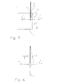
- the critical depth of penetration depends on the angle p, which includes the particular crystallographic direction K with the feed direction V in a plane perpendicular to the central longitudinal axis M of the single crystal. It has been found that the critical penetration depth on respective opposite sides S, S 'of the engaging blade 2 is different.
- FIG. 7 shows the critical penetration depth on the front side S opposite the cutting disk 2 and the rear side S 'for different angular settings p of the determined crystallographic direction K relative to the feed direction V.
- the resultant force F resulting from the sum of the constraining forces F x - , F x + and Fz is dependent on the feed direction V relative to the determined crystallographic direction K, ie the angle ⁇ include these two directions with each other in the parting plane perpendicular to the central longitudinal axis of the single crystal 1.
- the angle ⁇ include these two directions with each other in the parting plane perpendicular to the central longitudinal axis of the single crystal 1.
- the aforementioned constraining forces are used to correct the transverse deflection X of the cutting wheel during the cut.
- the deflection X of the cutting disk or the axial cutting force component F a or F b is measured by means of the sensor 6.
- the device 5 for rotating the monocrystal 1 is actuated via the control device 7 such that the angle p between the determined crystallographic direction K and the feed direction V is set so that the transverse deflection by means of the constraining forces F x - , F x + is controlled at substantially zero.
- the method is for the wire cutting apparatus shown in Figs. 3 and 4 equally applicable, in which case then the Deflection of one or more wires is measured.
- the preferred angles of particular crystallographic Direction K to the feed direction V, where the deflection of the cutting tool to cut to zero, are of the Material of the single crystal dependent. These angles are for each material of a single crystal empirically by means of a Test method determined.
- Fig. 11 is a single crystal 20 of a particular material in a plurality of discs 20a to 20e separated, the thickness thereof a plurality of thicknesses of the wafers to be produced later equivalent.
- the discs are then placed on a holder 21 glued so that their flat outer surface portions (Flats) 40a to 40e e.g. in a wire saw device in each case different angles to the feed direction V are arranged.
- the procedure is repeated until the preferred angles have been determined for optimal cutting are.
- the angles thus determined serve as a starting point for the Separation process later to be separated single crystals in the in the Fig. 1 to 4 shown devices, wherein the readjustment the adjustment of the angle on the device 5 and the Control device 7 for correction during the separation process serve.
- the apparatus shown in FIG. 12 is the adjusting device shown in FIG intended.
- the adjusting device has a base plate 50 and a vertically from this upwardly extending support 51 on.
- a Tab 52 provided, for example, on a non-illustrated Rail can be moved up and down in the vertical direction is and by means of a fastening device 53 in a predetermined height can be locked.
- the rider 52 points a projection 54 in the form of an angle, the lower edge 54a with the vertical includes a predetermined angle ⁇ .
- the single crystal 1 By pushing the single crystal 1 together the connector 55 and the bar 56 at the angle 54, the single crystal 1 is adjusted so that its level Outer surface portion 4 at the lower edge 54a of the angular Approach 54 is applied.
- the angle ⁇ , the lower edge 54a of the neck 54 forms with the vertical, is doing so chosen that for this specific single crystal 1 a certain preferred angle p between the particular crystallographic Set direction K to the vertical becomes.
- the feed direction V corresponds to the vertical, so that the angle ⁇ is defined.
- the invention described above has the particular advantage on that in particular GaAs wafer with a diameter of 6 inches or possibly even more easily with the inner hole saws can be disconnected because of an increased feed rate is possible.
- the invention is not for the separation of semiconductor single crystals (pure elements, semiconductors, semiconducting compounds) limited.
- inventive method and the Rather, devices can also be used to separate any single crystals, used as optical single crystals or ceramics become.
Abstract
Description
Die Erfindung betrifft ein Verfahren und eine Vorrichtung zum Trennen von Einkristallen, eine Justiervorrichtung und ein Testverfahren zum Ermitteln einer Orientierung eines Einkristalls für ein derartiges Verfahren.The invention relates to a method and a device for Separating single crystals, an adjusting device and a Test method for determining an orientation of a single crystal for such a procedure.
Zur Anwendung in der Halbleitertechnologie werden durch Kristallzüchten erzeugte Einkristalle in einzelne Scheiben, die als Wafer bezeichnet werden, getrennt. Bekannte Trennverfahren sind das Innenlochsägen und das Drahtsägen. Die beim Trennen der Einkristalle auftretenden Schnittkräfte führen zu einer seitlichen Auslenkung der Trennscheibe im Fall des Innenlochsägens bzw. des Drahtes im Fall des Drahtsägens. Dadurch wird eine ungleichmäßige Dicke des Wafers erzeugt oder die Oberfläche weist andere Ungleichmäßigkeiten z.B. Warp und Bow auf. Bei Siliziumeinkristallen tritt vor allen Dingen das Problem der Welligkeit der Oberfläche auf. Dies führt zu einer verminderten Qualität der erzeugten Wafer und somit zu einer geringeren Ausbeute an hochqualitativen Wafern. For use in semiconductor technology, crystal growing produced single crystals in individual disks, the as wafers, separated. Known separation process are inner hole sawing and wire sawing. The at Separating the single crystals occurring cutting forces lead to a lateral deflection of the cutting disc in the case of Innenlochsägens or the wire in the case of wire sawing. Thereby an uneven thickness of the wafer is produced or the surface has other irregularities, e.g. Warp and Bow up. In the case of silicon single crystals, this is especially true Problem of waviness of the surface. this leads to a reduced quality of the wafers produced and thus too a lower yield of high quality wafers.
Zur Lösung dieses Problemes ist es bekannt, beim Innenlochsägen die Auslenkung der Trennscheibe zu messen und durch Einwirkung von Druckluft zu korrigieren. Dieses Verfahren weist aber den Nachteil auf, daß ein zum Kühlen der Trennscheibe aufgebrachter Kühlmittelfilm durch die Druckluft beeinflußt wird, was sich wiederum auf die Kühlung beim Trennen auswirkt. Ferner ist es bekannt, den Einkristall in eine Halterung zu setzen, die speziell geformt ist, um den bei der Auslenkung der Trennscheibe auftretenden Kräften entsprechende Gegenkräfte zur Kompensation entgegen zu setzen. Beim Drahtsägen ist keine aktive Beeinflussung der Auslenkung des Drahtes möglich.To solve this problem, it is known in inner hole sawing to measure the deflection of the cutting disc and by action to correct for compressed air. This method points but the disadvantage that a for cooling the blade applied coolant film influenced by the compressed air which in turn affects the cooling during separation. Furthermore, it is known, the single crystal in a holder To put, which is specially shaped to the at the deflection corresponding to the blade occurring forces Counter forces to compensate. When wire sawing is not an active influence on the deflection of the wire possible.
Es ist Aufgabe der Erfindung, ein Verfahren und eine Vorrichtung zum Trennen von Einkristallen, eine Justiervorrichtung und ein Testverfahren zum Ermitteln einer Orientierung eines Einkristalls für ein derartiges Verfahren bereit zu stellen, mit dem bzw. mit der die oben genannten Probleme vermieden werden.It is an object of the invention, a method and an apparatus for separating single crystals, an adjusting device and a test method for determining an orientation of a Single crystal for such a process to provide with or with the above problems avoided become.
Die Aufgabe wird gelöst durch ein Verfahren nach Patentanspruch
1, eine Vorrichtung nach Patentanspruch 8, eine Vorrichtung
zum Justieren nach Patentanspruch 12 und ein Testverfahren
nach Patentanspruch 16.The object is achieved by a method according to
Weiterbildungen der Erfindung sind in den Unteransprüchen angegeben.Further developments of the invention are specified in the subclaims.
Das Verfahren und die Vorrichtung haben den Vorteil, daß die Qualität der Wafer erhöht wird und daß beim Trennen höhere Vorschubgeschwindigkeiten ermöglicht werden. Dadurch läßt sich insbesondere für GaAs das Innenlochsägen auch für Wafer von 6 Zoll Durchmesser und ggf. größer anwenden. Durch die verbesserte Qualität der erzeugten Wafer können sonst übliche Nachbearbeitungsschritte weitgehend entfallen.The method and the device have the advantage that the Quality of the wafer is increased and that when separating higher Feed rates are possible. Thereby leaves especially for GaAs inner hole sawing also for wafers of 6 inches in diameter and possibly larger. By the Improved quality of the produced wafers can be otherwise usual Post-processing steps largely eliminated.
Weitere Merkmale und Zweckmäßigkeiten der Erfindung ergeben sich aus der Beschreibung von Ausführungsbeispielen anhand der Figuren.Other features and advantages of the invention will be apparent from the description of embodiments based the figures.
Von den Figuren zeigen:
- Fig. 1
- eine schematische Darstellung in der Draufsicht in Richtung der Mittenlängsachse des Einkristalls einer Vorrichtung zum Innenlochsägen;
- Fig. 2
- eine schematische Seitenansicht einer Vorrichtung zum Innenlochsägen gemäß einer Ausführungsform der Erfindung;
- Fig. 3
- eine schematische Darstellung einer Vorrichtung zum Drahtsägen aus perspektivischer Sicht;
- Fig. 4
- eine schematische Darstellung einer Vorrichtung zum Drahtsägen entsprechend einer Ausführungsform der Erfindung in Seitenansicht;
- Fig. 5
- eine schematische Darstellung in Seitenansicht eines Wafers beim Innenlochsägen;
- Fig. 6
- eine Darstellung der beim Innenlochsägen auftretenden Kräfte;
- Fig. 7
- eine Darstellung kritischer Eindringtiefen für die Vernetzung von Mikrorissen in Abhängigkeit von einer Vorschubrichtung eines Trennwerkzeuges beim Trennen eines GaAs Einkristalls;
- Fig. 8
- eine Darstellung der Extremwerte der resultierenden Kraft der axialen Zwangskraftkomponenten, die zur Querauslenkung eines Trennwerkzeuges führt, in Abhängigkeit von der Vorschubrichtung des Trennwerkzeuges beim Trennen eines GaAs Einkristalls mittels Innenlochsägen;
- Fig. 9
- eine Darstellung des Warps des Wafers in Abhängigkeit von der Einstellung einer bestimmten Kristallrichtung zu einer Vorschubrichtung des Trennwerkzeuges am Beispiel von GaAs mittels Innenlochsägen;
- Fig. 10
- eine Darstellung der Rauhigkeit des Wafers in Abhängigkeit von der Einstellung der bestimmten Kristallrichtung zu einer Vorschubrichtung des Trennwerkzeuges am Beispiel von GaAs;
- Fig. 11
- eine schematische Darstellung eines Schrittes des erfindungsgemäßen Testverfahrens zum Ermitteln des optimalen Winkels der bestimmten Kristallrichtung zur Vorschubrichtung des Trennwerkzeuges für das Drahtsägen;
- Fig. 12
- eine schematische perspektivische Darstellung der Vorrichtung zum Justieren des Einkristalls.
- Fig. 1
- a schematic representation in plan view in the direction of the central longitudinal axis of the single crystal of a device for Innenlochsägen;
- Fig. 2
- a schematic side view of an apparatus for Innenlochsägen according to an embodiment of the invention;
- Fig. 3
- a schematic representation of a device for wire sawing from a perspective view;
- Fig. 4
- a schematic representation of a device for wire sawing according to an embodiment of the invention in side view;
- Fig. 5
- a schematic representation in side view of a wafer in Innenlochsägen;
- Fig. 6
- a representation of the forces occurring during Innenlochsägen;
- Fig. 7
- a representation of critical penetration depths for the crosslinking of microcracks in dependence on a feed direction of a separating tool when separating a GaAs single crystal;
- Fig. 8
- a representation of the extreme values of the resulting force of the axial force components that leads to the transverse deflection of a cutting tool, depending on the feed direction of the cutting tool when separating a GaAs single crystal by means of Innenlochsägen;
- Fig. 9
- a representation of the warp of the wafer as a function of the setting of a specific crystal direction to a feed direction of the cutting tool using the example of GaAs means Innenlochchsägen;
- Fig. 10
- a representation of the roughness of the wafer as a function of the setting of the specific crystal direction to a feed direction of the cutting tool using the example of GaAs;
- Fig. 11
- a schematic representation of a step of the test method according to the invention for determining the optimum angle of the determined crystal direction to the feed direction of the cutting tool for wire sawing;
- Fig. 12
- a schematic perspective view of the device for adjusting the single crystal.
Wie aus den Figuren 1 und 2 ersichtlich ist, weist eine erfindungsgemäße
Vorrichtung gemäß einer ersten Ausführungsform
der Erfindung eine Innenlochsägevorrichtung auf. Ein Einkristall
1 vom im wesentlichen zylindrischer Form mit einer Mittenlängsachse
M ist von einer nicht dargestellten Halterung
gehalten. Eine Innenlochtrennscheibe 2, die in bekannter
Weise aus einer Metallscheibe mit einem konzentrischen Loch
besteht, an dessen Begrenzung durch Aufbringen von Diamantkörnern
eine Schneidkante 3 gebildet ist, ist um eine Rotationsachse
R relativ zu dem Einkristall derart drehbar gelagert,
daß die Mittenlängsachse M des Einkristalls und die Rotationsachse
R der Trennscheibe parallel zueinander verlaufen.
Es ist ein nicht dargestellter Antrieb vorgesehen, mit
der die Trennscheibe 2 mit einer definierten Geschwindigkeit
um die Rotationsachse R in der in Fig. 1 dargestellten Richtung
A drehbar ist. Der Einkristall 1 ist über einen Antrieb
einer Vorschubeinheit in der in Fig. 2 dargestellten Vorschubrichtung
V in Richtung auf die Trennscheibe 2 derart bewegbar,
daß die Trennscheibe 2 den Einkristall 1 vollständig
in einer Ebene senkrecht zu seiner Mittenlängsachse M durchtrennen
kann. Ferner ist ein Antrieb vorgesehen zum Bewegen
des Einkristalls 1 senkrecht zur Trennscheibe 2 bzw. entlang
der Richtung seiner Mittenlängsachse mit einer Geschwindigkeit
w.As can be seen from Figures 1 and 2, an inventive
Device according to a first embodiment
The invention relates to a Innenlochsägevorrichtung. A
Wie insbesondere aus Fig. 1 ersichtlich ist, ist der Einkristall
1 nicht ganz zylinderförmig, sondern weist einen ebenen
Außenflächenabschnitt 4 auf, den sogenannten Flat, der derart
nach dem Züchten des Einkristalls 1 in definierter Weise angebracht
worden ist, daß ein Winkel α, den eine bestimmte
kristallographische Richtung K, für GaAs beispielsweise eine
[011]-Richtung, mit der Normalen N auf den ebenen Außenflächenabschnitt
4, in einer Ebene senkrecht zur Mittenlängsachse
M einschließt, bekannt ist. Da der Winkel α bekannt
ist, ist somit auch ein Winkel ρ zwischen der bestimmten kristallographischen
Richtung K und der Vorschubrichtung V des
Einkristalls in einer Ebene senkrecht zur Mittenlängsachse M
des Einkristalls und somit in der Trennebene T bekannt. Es
ist anzumerken, daß anstelle des Flats auch ein Notch genannter
Einschnitt an der Außenseite des Einkristalls vorgesehen
sein kann. Entscheidend ist lediglich ein äußeres Merkmal,
dessen Anordnung zur bestimmten kristallographischen Richtung
bekannt ist.As can be seen in particular from FIG. 1, the single crystal is
1 not completely cylindrical, but has a flat
Outside surface section 4, the so-called flat, the so
after culturing the
Wie in Fig. 2 gezeigt ist, weist die Vorrichtung ferner an
dem der Trennscheibe 2 abgewandten Ende des Einkristalls 1
eine Einrichtung 5 zum Drehen des Einkristalls 1 um seine
Mittenlängsachse M auf. Ferner ist ein Sensor 6 vorgesehen
zum Messen einer Auslenkung X der Trennscheibe 2 aus der
Trennebene T heraus beim Trennen eines scheibenförmigen Abschnitts
1a von dem Einkristall 1, der den späteren Wafer
bildet. Der Sensor 6 und die Einrichtung 5 zum Drehen des
Einkristalls 1 sind über eine Regeleinrichtung 7 miteinander
verbunden, die derart ausgebildet ist, daß in Abhängigkeit
von der gemessenen Auslenkung X der Trennscheibe 2 die Dreheinrichtung
5 betätigt wird, so daß der Einkristall 1 in eine
vorgegebenen azimutale Position gedreht wird, so daß die bestimmte
kristallographische Richtung K mit der Vorschubrichtung
V einen der gemessenen Auslenkung X der Trennscheibe 2
entsprechenden vordefinierten Winkel ρ einnimmt.As shown in Fig. 2, the apparatus further instructs
the end of the
In einer abgewandelten Ausführungsform ist die Vorrichtung
zum Trennen eines Einkristalls eine Drahtsägevorrichtung, wie
in den Figuren 3 und 4 gezeigt ist. Der in den Figuren 1 und
2 gezeigten Vorrichtung entsprechende Teile sind mit den
gleichen Bezugszeichen versehen. Wie in Fig. 3 gezeigt ist,
ist der Einkristall 1 in einer nicht dargestellten Halterung
gehalten, die über einen Antrieb einer Vorschubeinheit auf
das Drahtfeld einer Drahtsäge 8 hin und wieder zurück bewegbar
ist. Die Drahtsäge 8 besteht aus einer Vielzahl von
parallel verlaufenden Drähten 8a, 8b, 8c, die über nicht dargestellte
Rollen gespannt sind und in Ebenen senkrecht zur
Mittenlängsachse M des Einkristalls 1 in den durch Pfeile gezeigten
Richtungen A und B bewegbar sind. Die Vorrichtung umfaßt
ferner eine Vorrichtung 9 zum Aufbringen einer Paste,
welche Diamantkörner enthält, auf die Drähte 8a, 8b, 8c auf
einer Seite des Einkristalls 1 und eine Vorrichtung 10 zum
Reinigen der Drähte nach Durchtritt durch den Einkristall und
zum Austragen des Abtrages beim Durchgang der Drähte durch
den Einkristall. Alternativ ist das Diamantkorn bereits fest
in den Draht eingebunden und ein Aufbringen mittels einer
Paste ist nicht erforderlich. Analog zu der in Fig. 2 dargestellten
Vorrichtung weist diese Ausführungsform, wie in Fig.
4 dargestellt ist, ebenfalls eine Einrichtung 5 zum Drehen
des Einkristalls 1 und einen Sensor, der die Auslenkung eines
Drahtes 8a, 8b bzw. 8c erfaßt, und eine Regeleinrichtung 7
zum Steuern der Einrichtung 5 zum Drehen des Einkristalls 1
in Abhängigkeit von der erfaßten Drahtauslenkung auf.In a modified embodiment, the device
For separating a single crystal, a wire sawing device, such as
is shown in Figures 3 and 4. The in Figures 1 and
2 shown device corresponding parts are with the
provided the same reference numerals. As shown in FIG. 3,
is the
Der Betrieb der Vorrichtung gemäß den Figuren 1 und 2 wird nun im folgenden im Zusammenhang mit den Figuren 5 bis 10 beschrieben.The operation of the device according to Figures 1 and 2 is now in the following in connection with the figures 5 to 10 described.
Nach der Montage des Einkristalls 1 in der Halterung wird die
Halterung in der in Fig. 2 gezeigten Richtung W über den Antrieb
derart vorgeschoben, daß zwischen dem freien Ende 1a
des Einkristalls und der Trennscheibe 2 ein Abstand a verbleibt,
der etwas mehr als die Dicke eines zu erzeugenden Wafers
beträgt. Dann wird der Einkristall 1 über den Antrieb in
der in den Figuren 2 und 5 dargestellten Vorschubrichtung V
mit einer Vorschubgeschwindigkeit v gegen die Trennscheibe 2
bewegt, welche ihrerseits um ihre Rotationsachse in der in
Fig. 1 dargestellten Richtung A rotiert. Die rotierende
Trennscheibe 2 greift in den Einkristall 1 ein zum Abtrennen
eines Abschnittes 1a, der den späteren Wafer bildet, von dem
Einkristall 1. Die Diamantkörner der Schneidkante 3 der
Trennscheibe 2 erzeugen beim Trennvorgang nach dem Erreichen
einer kritischen Eindringtiefe in den Einkristall 1 Mikrorisse,
die durch gegenseite Vernetzung zum Materialabtrag
führen. Diese kritische Eindringtiefe hängt von der Bewegungsrichtung
des Korns zur bestimmten kristallographischen
Richtung K ab. Makroskopisch gesehen hängt die kritische Eindringtiefe
von dem Winkel p, den die bestimmte kristallographische
Richtung K mit der Vorschubrichtung V in einer Ebene
senkrecht zur Mittenlängsachse M des Einkristalls einschließt,
ab. Es wurde herausgefunden, daß die kritische Eindringtiefe
auf jeweils gegenüberliegenden Seiten S, S' der
eingreifenden Trennscheibe 2 liegen, unterschiedlich ist.
Fig. 7 zeigt die kritische Eindringtiefe auf der in Fig. 5
dargestellten, der Trennscheibe 2 gegenüberliegenden Vorderseite
S und der Rückseite S' für verschiedene Winkeleinstellungen
p der bestimmten kristallographischen Richtung K zur
Vorschubrichtung V. Diese unterschiedliche Eindringtiefe auf
Vorderseite S und Rückseite S' relativ zu der Trennscheibe 2
führt zu unterschiedlichen kritischen Lasten Lx - für die Vorderseite
S und Lx + für die Rückseite S'. Somit erfährt die
Schneidkante 3 unterschiedliche Zwangskräfte Fx -, Fx + von
Vorderseite S und Rückseite S', zusätzlich zu der in Vorschubrichtung
V wirkenden Zwangskraft Fz beim Auftreffen auf
das Material des Einkristalls 1, wie in Fig. 6 gezeigt ist.
Diese unterschiedlich großen richtungsabhängigen Zwangskräfte
Fx -, Fx + führen zu einer resultierenden Kraft F, die zu einer
richtungsabhängigen Querauslenkung X führt. After the assembly of the
Wie in Fig. 8 dargestellt ist, ist die resultierende Kraft F,
die aus der Summe der Zwangskräfte Fx -, Fx + und Fz entsteht,
abhängig von der Vorschubrichtung V relativ zu der bestimmten
kristallographischen Richtung K, d.h. dem Winkel ρ, den diese
beiden Richtungen miteinander in der Trennebene senkrecht zur
Mittenlängsachse des Einkristalls 1 einschließen. In Abhängigkeit
von dem Material des Einkristalls, bzw. bei Halbleitern
auch von der Dotierung, und von anderen Faktoren gibt es
bevorzugte Winkel, bei denen sich die o.g. Zwangskräfte kompensieren
und die Trennscheibe 2 ohne Querauslenkung in den
Einkristall 1 eindringt.As shown in FIG. 8, the resultant force F resulting from the sum of the constraining forces F x - , F x + and Fz is dependent on the feed direction V relative to the determined crystallographic direction K, ie the angle ρ include these two directions with each other in the parting plane perpendicular to the central longitudinal axis of the
Bei dem erfindungsgemäßen Verfahren werden die o.g. Zwangskräfte
zur Korrektur der Querauslenkung X der Trennscheibe
während des Schnittes genutzt. Hierzu wird, wie in Fig. 2
dargestellt ist, die Auslenkung X der Trennscheibe oder die
axiale Schnittkraftkomponente Fa bzw. Fb mittels des Sensors 6
gemessen. In Abhängigkeit von dem gemessenen Wert wird die
Einrichtung 5 zum Drehen des Einkristalls 1 über die Regeleinrichtung
7 derart betätigt, daß der Winkel p zwischen der
bestimmten kristallographischen Richtung K und der Vorschubrichtung
V so eingestellt wird, daß die Querauslenkung mittels
der Zwangskräfte Fx -, Fx + auf im wesentlichen Null geregelt
wird. In bestimmten Fällen ist es auch von Vorteil, die
Trennscheibe bzw. das Trennwerkzeug in definierter Weise
leicht auszulenken. Dies erfolgt ebenso durch Einstellen des
Winkels p.In the method according to the invention, the aforementioned constraining forces are used to correct the transverse deflection X of the cutting wheel during the cut. For this purpose, as shown in FIG. 2, the deflection X of the cutting disk or the axial cutting force component F a or F b is measured by means of the
Das Verfahren ist für die in den Fig. 3 und 4 gezeigte Drahtschneidevorrichtung genauso anwendbar, wobei dabei dann die Auslenkung eines oder mehrerer Drähte gemessen wird. The method is for the wire cutting apparatus shown in Figs. 3 and 4 equally applicable, in which case then the Deflection of one or more wires is measured.
Im Ergebnis erhält man, wie in den Fig. 9 und 10 gezeigt ist, mit Hilfe der Nutzung der Zwangskräfte für die aktive Beeinflussung der Querauslenkung eine Korrektur des Warps und der Rauhigkeit ra durch Drehen des Einkristalls um seine Mittenlängsachse M zur Einstellung eines bestimmten Winkels p zwischen der bestimmten kristallographischen Richtung K und der Vorschubrichtung V.As a result, as shown in Figs. 9 and 10, with the help of the use of coercive forces for active influence the transverse deflection a correction of the warps and the Roughness ra by turning the single crystal around its central longitudinal axis M for setting a certain angle p between the particular crystallographic direction K and the Feed direction V.
Die bevorzugten Winkel der bestimmten kristallographischen
Richtung K zur Vorschubrichtung V, bei denen die Auslenkung
des Trennwerkzeugs beim Schnitt zu Null wird, sind von dem
Material des Einkristalls abhängig. Diese Winkel werden für
jedes Material eines Einkristalls empirisch mittels eines
Testverfahrens ermittelt. Dabei wird, wie in Fig. 11 dargestellt
ist, ein Einkristall 20 eines bestimmten Materials in
eine Mehrzahl von Scheiben 20a bis 20e getrennt, deren Dicke
einer Mehrzahl von Dicken der später herzustellenden Wafer
entspricht. Die Scheiben werden anschließend auf eine Halterung
21 derart aufgeklebt, daß ihre ebenen Außenflächenabschnitte
(Flats) 40a bis 40e z.B. in einer Drahtsägevorrichtung
in jeweils unterschiedlichen Winkeln zur Vorschubrichtung
V angeordnet sind. Anschließend wird der so aus den
Scheiben 20a bis 20e zusammengesetzte Einkristall 20 in der
Trennvorrichtung gleichzeitig in einzelne Wafer getrennt und
die Waferoberflächen der so erhaltenen Wafer auf Rauhigkeit
und Warp vermessen. Das Verfahren wird so oft wiederholt, bis
die bevorzugten Winkel für optimales Trennen ermittelt worden
sind. Die so ermittelten Winkel dienen als Startgröße für den
Trennvorgang später zu trennender Einkristalle in den in den
Fig. 1 bis 4 gezeigten Vorrichtungen, wobei die Nachregelung
der Einstellung des Winkels über die Einrichtung 5 und die
Regeleinrichtung 7 zur Korrektur während des Trennvorganges
dienen. The preferred angles of particular crystallographic
Direction K to the feed direction V, where the deflection
of the cutting tool to cut to zero, are of the
Material of the single crystal dependent. These angles are for
each material of a single crystal empirically by means of a
Test method determined. In this case, as shown in Fig. 11
is a
Zum Einsetzen des Einkristalles 1 unter einem vorgegebenen
Winkel p zwischen der bestimmten kristallographischen Richtung
K und der Vorschubrichtung V in die in den Fig. 1 bis 4
gezeigten Vorrichtungen ist die in Fig. 12 dargestellte Justiervorrichtung
vorgesehen. Die Justiervorrichtung weist
eine Basisplatte 50 und einen sich von dieser vertikal nach
oben erstreckenden Träger 51 auf. Auf dem Träger 51 ist ein
Reiter 52 vorgesehen, der beispielsweise auf einer nicht dargestellten
Schiene in vertikaler Richtung auf und ab verschiebbar
ist und mittels einer Befestigungsvorrichtung 53 in
einer vorbestimmten Höhe arretierbar ist. Der Reiter 52 weist
einen Ansatz 54 in Form eines Winkels auf, dessen Unterkante
54a mit der Vertikalen einen vorbestimmten Winkel γ einschließt.
Beim Justieren wird der Einkristall 1, der mit
einem Verbindungsstück 55 zum Einsetzen des Einkristalls in
eine der in den Fig. 1 bis 4 gezeigten Trennvorrichtung fest
verbunden ist, auf eine Leiste 56, beispielsweise aus Graphit,
aufgeklebt, wobei der verwendete Klebstoff ein Klebstoff
ist, der erst nach einer vorbestimmten Zeit aushärtet,
so daß der Einkristall 1 auf der Leiste 56 noch für eine gewisse
Zeit um seine Mittenlängsachse M drehbar ist. Der Einkristall
1 wird sodann samt dem Verbindungsstück 55 und der
Leiste 56 in die Justiervorrichtung eingebracht, wobei der
Reiter 52 zuvor auf der für diesen Einkristalltyp erforderlichen
Höhe fixiert ist. Durch Schieben des Einkristalls 1 mitsamt
dem Verbindungsstück 55 und der Leiste 56 unter den Winkel
54 wird der Einkristall 1 so justiert, daß sein ebener
Außenflächenabschnitt 4 an der Unterkante 54a des winkelförmigen
Ansatzes 54 anliegt. Der Winkel γ, den die Unterkante
54a des Ansatzes 54 mit der Vertikalen bildet, ist dabei derart
gewählt, daß für diesen spezifischen Einkristall 1 ein
bestimmter bevorzugter Winkel p zwischen der bestimmten kristallographischen
Richtung K zu der Vertikalen eingestellt
wird. Nachdem der Einkristall 1 fest auf der Leiste 56 angekettet
ist, wird er in die Vorrichtung zum Trennen eingesetzt.
Die Vorschubrichtung V stimmt mit der Vertikalen überein,
so daß der Winkel ρ definiert ist.For inserting the
Die oben beschriebene Erfindung weist den besonderen Vorteil auf, daß damit insbesondere GaAs Wafer mit einem Durchmesser von 6 Zoll oder ggf. mehr noch problemlos mit dem Innenlochsägen getrennt werden können, weil eine erhöhte Vorschubgeschwindigkeit möglich ist.The invention described above has the particular advantage on that in particular GaAs wafer with a diameter of 6 inches or possibly even more easily with the inner hole saws can be disconnected because of an increased feed rate is possible.
Die Erfindung ist nicht auf das Trennen von Halbleitereinkristallen (reinen Elementen, Halbleitern, halbleitenden Verbindungen) beschränkt. Das erfindungsgemäße Verfahren und die Vorrichtung können vielmehr auch zum Trennen beliebiger Einkristalle, wie optischen Einkristallen oder Keramik eingesetzt werden.The invention is not for the separation of semiconductor single crystals (pure elements, semiconductors, semiconducting compounds) limited. The inventive method and the Rather, devices can also be used to separate any single crystals, used as optical single crystals or ceramics become.
Claims (17)
- A method for cutting single-crystal materials, in which a single crystal (1) to be cut into at least two parts and a cutting tool (2, 3; 8, 8a, 8b, 8c) are moved relative to one another in a direction of feed (V), and in which the single crystal (1) is oriented such that a particular crystallographic direction (K) lies in the plane (T) of cutting, characterised in that an angle (ρ) between the particular crystallographic direction (K) and the direction of feed (V) is selected such that forces which during cutting act on the cutting tool in a direction perpendicular to the plane (T) of cutting compensate one another or add up to a predetermined force.
- A method according to Claim 1, characterised in that a deflection (X) of the cutting tool (2, 3; 8, 8a, 8b, 8c) is measured during cutting and the single crystal (1) is rotated as a function of the measured value with respect to the particular crystallographic direction (K) in the plane (T) of cutting.
- A method according to Claim 1 or 2, characterised in that the cutting is performed by means of inner diameter sawing.
- A method according to Claim 1 or 2, characterised in that the cutting is performed by means of wire sawing.
- A method according to one of Claims 1 to 4, characterised in that the angle (p) is determined empirically before cutting.
- A method according to one of Claims 1 to 5, characterised in that the angle (ρ is adjusted by way of an adjustment device outside the actual cutting device.
- A method according to one of Claims 1 to 6, characterised in that the method is used to cut single crystals (1) of III-V semiconductors, in particular GaAs.
- A device for cutting single crystals, having a cutting tool (2, 3; 8, 8a, 8b, 8c), a holder for the single crystal (1), a drive for moving the holder and the cutting tool relative to one another in a direction of feed (V) which extends perpendicular to the centre longitudinal axis (M) of the single crystal (1), and a rotation device (5) for rotating the holder, by means of which the holder is rotatable such that the single crystal (1) can be rotated about its centre longitudinal axis (M), characterised by a measuring device (6) for measuring a deflection (X) of the cutting tool in a direction perpendicular to the direction of feed (V).
- A device according to Claim 8, characterised by a regulating device which is connected to the measuring device (6) and the rotation device (5) and which controls the rotation device (5) such that the single crystal is rotated such that the deflection of the cutting tool substantially reaches 0 or a predetermined value.
- A device according to Claim 8 or 9, characterised in that the device is an inner diameter sawing device.
- A device according to Claim 8 or 9, characterised in that the device is a wire sawing device.
- A device for adjusting a single crystal, in which the single crystal (1) is constructed to be substantially cylindrical and has a centre longitudinal axis (M), and in which the single crystal has a planar outer face portion (4), and a particular crystallographic direction (K) of the single crystal is at a known angle (α) to the normal (N) on the planar outer face portion in a plane perpendicular to the centre longitudinal axis (M), having a stop which is provided on a vertically aligned support (51) and has a lower edge (54) which forms a predetermined angle (γ) with the vertical.
- A device according to Claim 12, characterised in that the stop is adjustable in height.
- A device according to Claim 12 or 13, characterised in that different exchangeable stops having different angles (γ) are provided.
- A device according to one of Claims 12 to 14, characterised in that the device is an adjustment device for carrying out the method according to one of Claims 1 to 8.
- A test method for determining the optimum angle between the particular crystallographic direction (K) and the direction of feed (V) of the method according to one of Claims 1o to 8, having the steps of
cutting a single crystal, in which the single crystal is constructed to be substantially cylindrical and has a centre longitudinal axis (M), and in which the single crystal has an external feature (4) whereof the orientation with respect to a particular crystallographic direction (K) of the single crystal is known, into a plurality of portions (20a to 20e) of predetermined thickness perpendicular to the centre longitudinal axis, connecting the portions such that the external feature of each portion adopts a different azimuthal position with respect to the centre longitudinal axis (M),
in a cutting device, simultaneously cutting the single crystal (20) composed in this way into slices having the thickness of a wafer to be made later,
measuring the surface planarity and/or thickness of the slices thus produced, determining the optimum angle (p) of the particular crystallographic direction (K) in relation to a direction of feed (V) of a cutting tool. - A test method according to Claim 16, characterised in that the external feature is a flat or a notch.
Applications Claiming Priority (3)
| Application Number | Priority Date | Filing Date | Title |
|---|---|---|---|
| DE10052154 | 2000-10-20 | ||
| DE10052154A DE10052154A1 (en) | 2000-10-20 | 2000-10-20 | Method and device for separating single crystals, adjusting device and test method for determining an orientation of a single crystal for such a method |
| PCT/EP2001/008800 WO2002034973A1 (en) | 2000-10-20 | 2001-07-30 | Method and device for cutting single crystals, in addition to an adjusting device and a test method for determining a crystal orientation |
Publications (2)
| Publication Number | Publication Date |
|---|---|
| EP1332247A1 EP1332247A1 (en) | 2003-08-06 |
| EP1332247B1 true EP1332247B1 (en) | 2004-09-29 |
Family
ID=7660519
Family Applications (1)
| Application Number | Title | Priority Date | Filing Date |
|---|---|---|---|
| EP01960587A Expired - Lifetime EP1332247B1 (en) | 2000-10-20 | 2001-07-30 | Method and device for cutting single crystals, in addition to an adjusting device and a test method for determining a crystal orientation |
Country Status (11)
| Country | Link |
|---|---|
| US (1) | US7137865B2 (en) |
| EP (1) | EP1332247B1 (en) |
| JP (1) | JP5087202B2 (en) |
| CN (1) | CN1270000C (en) |
| AT (1) | ATE278052T1 (en) |
| CZ (1) | CZ297783B6 (en) |
| DE (2) | DE10052154A1 (en) |
| RU (1) | RU2251598C2 (en) |
| SK (1) | SK286535B6 (en) |
| TW (1) | TW521340B (en) |
| WO (1) | WO2002034973A1 (en) |
Families Citing this family (20)
| Publication number | Priority date | Publication date | Assignee | Title |
|---|---|---|---|---|
| DE10128630A1 (en) | 2001-06-13 | 2003-01-02 | Freiberger Compound Mat Gmbh | Device and method for determining the orientation of a crystallographic plane relative to a crystal surface and device and method for separating a single crystal in a separating machine |
| JP4525353B2 (en) * | 2005-01-07 | 2010-08-18 | 住友電気工業株式会社 | Method for manufacturing group III nitride substrate |
| DE102005040343A1 (en) | 2005-08-25 | 2007-03-01 | Freiberger Compound Materials Gmbh | Wire saw for cutting glass has device for presetting water content of gas surrounding at least part of slurry |
| EP1757419B1 (en) | 2005-08-25 | 2012-10-17 | Freiberger Compound Materials GmbH | Method, apparatus and slurry for wire sawing |
| KR101230276B1 (en) * | 2007-06-25 | 2013-02-06 | 생-고뱅 세라믹스 앤드 플라스틱스, 인코포레이티드 | Methods of crystallographically reorienting single crystal bodies |
| JP5152199B2 (en) * | 2007-12-19 | 2013-02-27 | 旭硝子株式会社 | Ether composition |
| WO2010006148A2 (en) * | 2008-07-11 | 2010-01-14 | Saint-Gobain Abrasives. Inc. | Wire slicing system |
| CN101486231B (en) * | 2009-01-22 | 2011-12-07 | 四川大学 | Oriented cutting method for preparing infrared non-linear optics element from yellow copper uniaxial negative crystal |
| DE102010018570B4 (en) * | 2010-04-28 | 2017-06-08 | Siltronic Ag | A method of manufacturing a plurality of semiconductor wafers by processing a single crystal |
| US8259901B1 (en) | 2010-05-25 | 2012-09-04 | Rubicon Technology, Inc. | Intelligent machines and process for production of monocrystalline products with goniometer continual feedback |
| JP2012045682A (en) * | 2010-08-27 | 2012-03-08 | Tokuriki Honten Co Ltd | Fixed abrasive grain wire saw device |
| CN102152410A (en) * | 2010-12-23 | 2011-08-17 | 万向硅峰电子股份有限公司 | Cutting method for adjusting crystal orientation excursion by rotating single crystal rod |
| DE112012002299T5 (en) * | 2011-06-02 | 2014-05-15 | Sumitomo Electric Industries, Ltd. | Method for producing a silicon carbide substrate |
| US10052848B2 (en) | 2012-03-06 | 2018-08-21 | Apple Inc. | Sapphire laminates |
| US9154678B2 (en) | 2013-12-11 | 2015-10-06 | Apple Inc. | Cover glass arrangement for an electronic device |
| JP6000235B2 (en) | 2013-12-24 | 2016-09-28 | 信越半導体株式会社 | Work cutting method and work holding jig |
| US10406634B2 (en) | 2015-07-01 | 2019-09-10 | Apple Inc. | Enhancing strength in laser cutting of ceramic components |
| JP6613482B2 (en) * | 2015-09-03 | 2019-12-04 | 日本電波工業株式会社 | Crystal oscillator |
| CN111638305B (en) * | 2020-06-08 | 2023-09-22 | 郑州磨料磨具磨削研究所有限公司 | Method for determining optimal processing direction of monocrystalline material |
| CN112590032B (en) * | 2020-12-03 | 2022-12-02 | 天津市环智新能源技术有限公司 | Solar silicon wafer and roughness control method thereof |
Family Cites Families (21)
| Publication number | Priority date | Publication date | Assignee | Title |
|---|---|---|---|---|
| GB628508A (en) * | 1947-05-06 | 1949-08-30 | Standard Telephones Cables Ltd | Improvements in or relating to machines for cutting crystalline material |
| JPS56129114A (en) * | 1980-03-17 | 1981-10-09 | Tokyo Shibaura Electric Co | Method of cutting monocrystal |
| JPH0761647B2 (en) * | 1985-06-11 | 1995-07-05 | 日立電線株式会社 | Slicing method of semiconductor crystal ingot |
| DE3640645A1 (en) | 1986-11-28 | 1988-06-09 | Wacker Chemitronic | METHOD FOR SAWING CRYSTAL RODS OR BLOCKS BY MEANS OF INTERNAL HOLE SAWS IN THIN WINDOWS |
| JPH0635107B2 (en) * | 1987-12-26 | 1994-05-11 | 株式会社タカトリハイテック | Wire saw |
| JP2655677B2 (en) * | 1988-04-26 | 1997-09-24 | トーヨーエイテック株式会社 | Slicing machine |
| DE3826698A1 (en) * | 1988-08-05 | 1990-02-08 | Wacker Chemitronic | METHOD AND DEVICE FOR CONTROLLING THE CUTTING PROCESS WHEN DISCONNECTING DISKS FROM NON-MAGNETIZABLE WORKPIECES |
| US5131975A (en) * | 1990-07-10 | 1992-07-21 | The Regents Of The University Of California | Controlled growth of semiconductor crystals |
| CH690845A5 (en) * | 1994-05-19 | 2001-02-15 | Tokyo Seimitsu Co Ltd | A method for positioning a workpiece, and apparatus therefor. |
| CH690422A5 (en) | 1995-04-22 | 2000-09-15 | Hct Shaping Systems Sa | Monocrystal positioning procedure for cutting, e.g. for optical applications or semi-conductors |
| EP0738572B1 (en) * | 1995-04-22 | 2004-01-21 | HCT Shaping Systems SA | Method for orienting monocrystals for cutting in a cutting machine and device for performing the method |
| JP2842307B2 (en) | 1995-06-30 | 1999-01-06 | 住友電気工業株式会社 | Method for cutting III-V compound semiconductor crystal |
| JPH0985736A (en) * | 1995-09-22 | 1997-03-31 | Toray Eng Co Ltd | Wire type cutting device |
| CH691045A5 (en) | 1996-04-16 | 2001-04-12 | Hct Shaping Systems Sa | A method for the orientation of several crystalline parts placed side by side on a cutting support for a simultaneous cutting in a cutting machine and device for |
| CH690907A5 (en) * | 1996-05-23 | 2001-02-28 | Hct Shaping Systems Sa | Wire sawing device |
| CH692331A5 (en) * | 1996-06-04 | 2002-05-15 | Tokyo Seimitsu Co Ltd | Wire saw and cutting method using the same. |
| JPH1110510A (en) * | 1997-06-19 | 1999-01-19 | Nippei Toyama Corp | Wire saw device and method for cutting workpiece |
| US5878737A (en) * | 1997-07-07 | 1999-03-09 | Laser Technology West Limited | Apparatus and method for slicing a workpiece utilizing a diamond impregnated wire |
| JP3205718B2 (en) | 1997-08-29 | 2001-09-04 | 株式会社スーパーシリコン研究所 | Wire saw cutting method and device |
| JPH11235718A (en) * | 1998-02-20 | 1999-08-31 | Hitachi Cable Ltd | Method for cutting semiconductor ingot |
| DE19825051A1 (en) * | 1998-06-04 | 1999-12-09 | Wacker Siltronic Halbleitermat | Method and device for producing a cylindrical single crystal and method for separating semiconductor wafers |
-
2000
- 2000-10-20 DE DE10052154A patent/DE10052154A1/en not_active Ceased
-
2001
- 2001-07-30 DE DE50103912T patent/DE50103912D1/en not_active Expired - Lifetime
- 2001-07-30 US US10/399,672 patent/US7137865B2/en not_active Expired - Lifetime
- 2001-07-30 SK SK450-2003A patent/SK286535B6/en not_active IP Right Cessation
- 2001-07-30 CZ CZ20031102A patent/CZ297783B6/en not_active IP Right Cessation
- 2001-07-30 EP EP01960587A patent/EP1332247B1/en not_active Expired - Lifetime
- 2001-07-30 RU RU2003114430/15A patent/RU2251598C2/en active
- 2001-07-30 AT AT01960587T patent/ATE278052T1/en not_active IP Right Cessation
- 2001-07-30 CN CNB018176313A patent/CN1270000C/en not_active Expired - Lifetime
- 2001-07-30 WO PCT/EP2001/008800 patent/WO2002034973A1/en active IP Right Grant
- 2001-07-30 JP JP2002537937A patent/JP5087202B2/en not_active Expired - Lifetime
- 2001-10-04 TW TW090124464A patent/TW521340B/en not_active IP Right Cessation
Also Published As
| Publication number | Publication date |
|---|---|
| RU2251598C2 (en) | 2005-05-10 |
| US20040118338A1 (en) | 2004-06-24 |
| US7137865B2 (en) | 2006-11-21 |
| SK286535B6 (en) | 2008-12-05 |
| ATE278052T1 (en) | 2004-10-15 |
| WO2002034973A1 (en) | 2002-05-02 |
| SK4502003A3 (en) | 2003-11-04 |
| CZ297783B6 (en) | 2007-03-28 |
| DE10052154A1 (en) | 2002-05-08 |
| CZ20031102A3 (en) | 2003-09-17 |
| JP2004512251A (en) | 2004-04-22 |
| TW521340B (en) | 2003-02-21 |
| DE50103912D1 (en) | 2004-11-04 |
| CN1270000C (en) | 2006-08-16 |
| CN1469942A (en) | 2004-01-21 |
| EP1332247A1 (en) | 2003-08-06 |
| JP5087202B2 (en) | 2012-12-05 |
Similar Documents
| Publication | Publication Date | Title |
|---|---|---|
| EP1332247B1 (en) | Method and device for cutting single crystals, in addition to an adjusting device and a test method for determining a crystal orientation | |
| DE69734414T2 (en) | Process for cutting a single crystal ingot of semiconductor material | |
| DE102008051673B4 (en) | A method for simultaneously separating a composite rod of silicon into a plurality of disks | |
| EP1568457A1 (en) | Device and method for determining the orientation of a crystallographic plane in relation to a crystal surface | |
| DE102005047114A1 (en) | Grinding process and apparatus with an arrangement for grinding with a constant grinding load | |
| DE3906091A1 (en) | METHOD FOR SAWING ROD-SHAPED WORKPIECES IN DISKS BY MEANS OF INTERNAL HOLE SAWS, AND ITS IMPLEMENTATION | |
| DE3613132A1 (en) | METHOD FOR DIVIDING HARD, NON-METAL MATERIALS | |
| DE19825051A1 (en) | Method and device for producing a cylindrical single crystal and method for separating semiconductor wafers | |
| DE2355339B2 (en) | Precision holding device for cylindrical workpieces | |
| DE102012017662A1 (en) | Sample holder for grinding device of sample preparation device, comprises replaceable sacrificial stop elements vertically adjustable in normal direction, where grinding plane lying parallel to plane is formed by sacrificial stop elements | |
| DE102007028439A1 (en) | Separating flat-parallel silicon wafers from cuboid crystalline or polycrystalline silicon ingot using wire saw for photo-voltaic applications, comprises moving wire around rolls, and attaching the ingot to reception of the wire saw | |
| EP0432637B1 (en) | Device for dressing the cutting edge of a cutting-off tool for severing slices from an ingot or block-like workpiece, especially semiconductor material, use and sewing method for the same | |
| DE212017000282U1 (en) | Cutter with cassette and an improved cassette attachment device therefor | |
| DE102010007459B4 (en) | A method of separating a plurality of slices from a crystal of semiconductor material | |
| DE19526711A1 (en) | Silicon@ wafer mfr. for VLSI mfr. | |
| EP0464668B1 (en) | Tensioning device for an inner diameter saw blade and its use for sawing rods, in particular from semiconductor material, into wafers | |
| EP0204958B1 (en) | Apparatus for grinding and lapping sealing surfaces of gate valves and the like in-situ or in the shop | |
| EP0791444B1 (en) | Wafer manufacturing process | |
| DE19825050C2 (en) | Method for arranging and orienting single crystals for cutting off wafers on a wire saw having a wire frame | |
| EP2765617A2 (en) | Method for producing wafers, in particular wafers for solar cells, and device for producing wafers | |
| DE4321048C2 (en) | Holding device and method for producing glazing beads | |
| DE102012220952A1 (en) | Method of machining edge of semiconductor wafer, involves using grinding tool with abrasive having grain size that is less than first particle size, and processing semiconductor wafer with grinding wheel pf specific rotational speed | |
| EP0014270B1 (en) | Method and device for forming cutter-head edges on a tempered tool | |
| DE102005038639B4 (en) | Method and device for measuring, aligning and fixing and fixing single crystals on a common carrier | |
| DE2052386A1 (en) | Cutting body, in particular for a machine tool, and method for its production |
Legal Events
| Date | Code | Title | Description |
|---|---|---|---|
| PUAI | Public reference made under article 153(3) epc to a published international application that has entered the european phase |
Free format text: ORIGINAL CODE: 0009012 |
|
| 17P | Request for examination filed |
Effective date: 20030307 |
|
| AK | Designated contracting states |
Designated state(s): AT BE CH CY DE DK ES FI FR GB GR IE IT LI LU MC NL PT SE TR |
|
| GRAP | Despatch of communication of intention to grant a patent |
Free format text: ORIGINAL CODE: EPIDOSNIGR1 |
|
| GRAS | Grant fee paid |
Free format text: ORIGINAL CODE: EPIDOSNIGR3 |
|
| GRAA | (expected) grant |
Free format text: ORIGINAL CODE: 0009210 |
|
| AK | Designated contracting states |
Kind code of ref document: B1 Designated state(s): AT BE CH CY DE DK ES FI FR GB GR IE IT LI LU MC NL PT SE TR |
|
| PG25 | Lapsed in a contracting state [announced via postgrant information from national office to epo] |
Ref country code: TR Free format text: LAPSE BECAUSE OF FAILURE TO SUBMIT A TRANSLATION OF THE DESCRIPTION OR TO PAY THE FEE WITHIN THE PRESCRIBED TIME-LIMIT Effective date: 20040929 Ref country code: NL Free format text: LAPSE BECAUSE OF FAILURE TO SUBMIT A TRANSLATION OF THE DESCRIPTION OR TO PAY THE FEE WITHIN THE PRESCRIBED TIME-LIMIT Effective date: 20040929 Ref country code: IE Free format text: LAPSE BECAUSE OF FAILURE TO SUBMIT A TRANSLATION OF THE DESCRIPTION OR TO PAY THE FEE WITHIN THE PRESCRIBED TIME-LIMIT Effective date: 20040929 Ref country code: FI Free format text: LAPSE BECAUSE OF FAILURE TO SUBMIT A TRANSLATION OF THE DESCRIPTION OR TO PAY THE FEE WITHIN THE PRESCRIBED TIME-LIMIT Effective date: 20040929 |
|
| REG | Reference to a national code |
Ref country code: GB Ref legal event code: FG4D Free format text: NOT ENGLISH |
|
| REG | Reference to a national code |
Ref country code: CH Ref legal event code: EP |
|
| REG | Reference to a national code |
Ref country code: CH Ref legal event code: NV Representative=s name: NOVAGRAAF INTERNATIONAL SA |
|
| GBT | Gb: translation of ep patent filed (gb section 77(6)(a)/1977) | ||
| REG | Reference to a national code |
Ref country code: IE Ref legal event code: FG4D Free format text: GERMAN |
|
| REF | Corresponds to: |
Ref document number: 50103912 Country of ref document: DE Date of ref document: 20041104 Kind code of ref document: P |
|
| PG25 | Lapsed in a contracting state [announced via postgrant information from national office to epo] |
Ref country code: SE Free format text: LAPSE BECAUSE OF FAILURE TO SUBMIT A TRANSLATION OF THE DESCRIPTION OR TO PAY THE FEE WITHIN THE PRESCRIBED TIME-LIMIT Effective date: 20041229 Ref country code: GR Free format text: LAPSE BECAUSE OF FAILURE TO SUBMIT A TRANSLATION OF THE DESCRIPTION OR TO PAY THE FEE WITHIN THE PRESCRIBED TIME-LIMIT Effective date: 20041229 Ref country code: DK Free format text: LAPSE BECAUSE OF FAILURE TO SUBMIT A TRANSLATION OF THE DESCRIPTION OR TO PAY THE FEE WITHIN THE PRESCRIBED TIME-LIMIT Effective date: 20041229 |
|
| PG25 | Lapsed in a contracting state [announced via postgrant information from national office to epo] |
Ref country code: ES Free format text: LAPSE BECAUSE OF FAILURE TO SUBMIT A TRANSLATION OF THE DESCRIPTION OR TO PAY THE FEE WITHIN THE PRESCRIBED TIME-LIMIT Effective date: 20050109 |
|
| NLV1 | Nl: lapsed or annulled due to failure to fulfill the requirements of art. 29p and 29m of the patents act | ||
| REG | Reference to a national code |
Ref country code: IE Ref legal event code: FD4D |
|
| ET | Fr: translation filed | ||
| PGFP | Annual fee paid to national office [announced via postgrant information from national office to epo] |
Ref country code: AT Payment date: 20050628 Year of fee payment: 5 |
|
| PG25 | Lapsed in a contracting state [announced via postgrant information from national office to epo] |
Ref country code: LU Free format text: LAPSE BECAUSE OF NON-PAYMENT OF DUE FEES Effective date: 20050730 Ref country code: CY Free format text: LAPSE BECAUSE OF FAILURE TO SUBMIT A TRANSLATION OF THE DESCRIPTION OR TO PAY THE FEE WITHIN THE PRESCRIBED TIME-LIMIT Effective date: 20050730 |
|
| PG25 | Lapsed in a contracting state [announced via postgrant information from national office to epo] |
Ref country code: MC Free format text: LAPSE BECAUSE OF NON-PAYMENT OF DUE FEES Effective date: 20050731 |
|
| PLBE | No opposition filed within time limit |
Free format text: ORIGINAL CODE: 0009261 |
|
| STAA | Information on the status of an ep patent application or granted ep patent |
Free format text: STATUS: NO OPPOSITION FILED WITHIN TIME LIMIT |
|
| 26N | No opposition filed |
Effective date: 20050630 |
|
| PG25 | Lapsed in a contracting state [announced via postgrant information from national office to epo] |
Ref country code: AT Free format text: LAPSE BECAUSE OF NON-PAYMENT OF DUE FEES Effective date: 20060730 |
|
| PG25 | Lapsed in a contracting state [announced via postgrant information from national office to epo] |
Ref country code: PT Free format text: LAPSE BECAUSE OF NON-PAYMENT OF DUE FEES Effective date: 20050228 |
|
| REG | Reference to a national code |
Ref country code: CH Ref legal event code: PFA Owner name: FREIBERGER COMPOUND MATERIALS GMBH Free format text: FREIBERGER COMPOUND MATERIALS GMBH#AM JUNGER LOEWE SCHACHT 5#09599 FREIBERG (DE) -TRANSFER TO- FREIBERGER COMPOUND MATERIALS GMBH#AM JUNGER LOEWE SCHACHT 5#09599 FREIBERG (DE) |
|
| REG | Reference to a national code |
Ref country code: FR Ref legal event code: PLFP Year of fee payment: 16 |
|
| REG | Reference to a national code |
Ref country code: FR Ref legal event code: PLFP Year of fee payment: 17 |
|
| REG | Reference to a national code |
Ref country code: FR Ref legal event code: PLFP Year of fee payment: 18 |
|
| PGFP | Annual fee paid to national office [announced via postgrant information from national office to epo] |
Ref country code: DE Payment date: 20200729 Year of fee payment: 20 Ref country code: FR Payment date: 20200727 Year of fee payment: 20 Ref country code: GB Payment date: 20200724 Year of fee payment: 20 |
|
| PGFP | Annual fee paid to national office [announced via postgrant information from national office to epo] |
Ref country code: BE Payment date: 20200722 Year of fee payment: 20 Ref country code: CH Payment date: 20200724 Year of fee payment: 20 Ref country code: IT Payment date: 20200731 Year of fee payment: 20 |
|
| REG | Reference to a national code |
Ref country code: DE Ref legal event code: R071 Ref document number: 50103912 Country of ref document: DE |
|
| REG | Reference to a national code |
Ref country code: CH Ref legal event code: PL |
|
| REG | Reference to a national code |
Ref country code: BE Ref legal event code: MK Effective date: 20210730 Ref country code: GB Ref legal event code: PE20 Expiry date: 20210729 |
|
| PG25 | Lapsed in a contracting state [announced via postgrant information from national office to epo] |
Ref country code: GB Free format text: LAPSE BECAUSE OF EXPIRATION OF PROTECTION Effective date: 20210729 |