EP1331664A1 - Semiconductor device and its manufacturing method - Google Patents
Semiconductor device and its manufacturing method Download PDFInfo
- Publication number
- EP1331664A1 EP1331664A1 EP01980950A EP01980950A EP1331664A1 EP 1331664 A1 EP1331664 A1 EP 1331664A1 EP 01980950 A EP01980950 A EP 01980950A EP 01980950 A EP01980950 A EP 01980950A EP 1331664 A1 EP1331664 A1 EP 1331664A1
- Authority
- EP
- European Patent Office
- Prior art keywords
- layer
- underlying layer
- copper
- semiconductor device
- underlying
- Prior art date
- Legal status (The legal status is an assumption and is not a legal conclusion. Google has not performed a legal analysis and makes no representation as to the accuracy of the status listed.)
- Withdrawn
Links
Images





Classifications
-
- H—ELECTRICITY
- H10—SEMICONDUCTOR DEVICES; ELECTRIC SOLID-STATE DEVICES NOT OTHERWISE PROVIDED FOR
- H10W—GENERIC PACKAGES, INTERCONNECTIONS, CONNECTORS OR OTHER CONSTRUCTIONAL DETAILS OF DEVICES COVERED BY CLASS H10
- H10W20/00—Interconnections in chips, wafers or substrates
- H10W20/01—Manufacture or treatment
-
- H—ELECTRICITY
- H10—SEMICONDUCTOR DEVICES; ELECTRIC SOLID-STATE DEVICES NOT OTHERWISE PROVIDED FOR
- H10W—GENERIC PACKAGES, INTERCONNECTIONS, CONNECTORS OR OTHER CONSTRUCTIONAL DETAILS OF DEVICES COVERED BY CLASS H10
- H10W20/00—Interconnections in chips, wafers or substrates
- H10W20/01—Manufacture or treatment
- H10W20/031—Manufacture or treatment of conductive parts of the interconnections
- H10W20/032—Manufacture or treatment of conductive parts of the interconnections of conductive barrier, adhesion or liner layers
- H10W20/033—Manufacture or treatment of conductive parts of the interconnections of conductive barrier, adhesion or liner layers in openings in dielectrics
- H10W20/035—Manufacture or treatment of conductive parts of the interconnections of conductive barrier, adhesion or liner layers in openings in dielectrics combinations of barrier, adhesion or liner layers, e.g. multi-layered barrier layers
-
- H—ELECTRICITY
- H10—SEMICONDUCTOR DEVICES; ELECTRIC SOLID-STATE DEVICES NOT OTHERWISE PROVIDED FOR
- H10W—GENERIC PACKAGES, INTERCONNECTIONS, CONNECTORS OR OTHER CONSTRUCTIONAL DETAILS OF DEVICES COVERED BY CLASS H10
- H10W20/00—Interconnections in chips, wafers or substrates
- H10W20/01—Manufacture or treatment
- H10W20/031—Manufacture or treatment of conductive parts of the interconnections
- H10W20/032—Manufacture or treatment of conductive parts of the interconnections of conductive barrier, adhesion or liner layers
- H10W20/042—Manufacture or treatment of conductive parts of the interconnections of conductive barrier, adhesion or liner layers the barrier, adhesion or liner layers being seed or nucleation layers
- H10W20/043—Manufacture or treatment of conductive parts of the interconnections of conductive barrier, adhesion or liner layers the barrier, adhesion or liner layers being seed or nucleation layers for electroplating
-
- H—ELECTRICITY
- H10—SEMICONDUCTOR DEVICES; ELECTRIC SOLID-STATE DEVICES NOT OTHERWISE PROVIDED FOR
- H10W—GENERIC PACKAGES, INTERCONNECTIONS, CONNECTORS OR OTHER CONSTRUCTIONAL DETAILS OF DEVICES COVERED BY CLASS H10
- H10W20/00—Interconnections in chips, wafers or substrates
- H10W20/01—Manufacture or treatment
- H10W20/031—Manufacture or treatment of conductive parts of the interconnections
- H10W20/032—Manufacture or treatment of conductive parts of the interconnections of conductive barrier, adhesion or liner layers
- H10W20/047—Manufacture or treatment of conductive parts of the interconnections of conductive barrier, adhesion or liner layers by introducing additional elements therein
- H10W20/049—Manufacture or treatment of conductive parts of the interconnections of conductive barrier, adhesion or liner layers by introducing additional elements therein by diffusing alloying elements
-
- H—ELECTRICITY
- H10—SEMICONDUCTOR DEVICES; ELECTRIC SOLID-STATE DEVICES NOT OTHERWISE PROVIDED FOR
- H10W—GENERIC PACKAGES, INTERCONNECTIONS, CONNECTORS OR OTHER CONSTRUCTIONAL DETAILS OF DEVICES COVERED BY CLASS H10
- H10W20/00—Interconnections in chips, wafers or substrates
- H10W20/01—Manufacture or treatment
- H10W20/031—Manufacture or treatment of conductive parts of the interconnections
- H10W20/032—Manufacture or treatment of conductive parts of the interconnections of conductive barrier, adhesion or liner layers
- H10W20/055—Manufacture or treatment of conductive parts of the interconnections of conductive barrier, adhesion or liner layers by formation methods other than physical vapour deposition [PVD], chemical vapour deposition [CVD] or liquid deposition
-
- H—ELECTRICITY
- H10—SEMICONDUCTOR DEVICES; ELECTRIC SOLID-STATE DEVICES NOT OTHERWISE PROVIDED FOR
- H10W—GENERIC PACKAGES, INTERCONNECTIONS, CONNECTORS OR OTHER CONSTRUCTIONAL DETAILS OF DEVICES COVERED BY CLASS H10
- H10W20/00—Interconnections in chips, wafers or substrates
- H10W20/40—Interconnections external to wafers or substrates, e.g. back-end-of-line [BEOL] metallisations or vias connecting to gate electrodes
- H10W20/41—Interconnections external to wafers or substrates, e.g. back-end-of-line [BEOL] metallisations or vias connecting to gate electrodes characterised by their conductive parts
- H10W20/425—Barrier, adhesion or liner layers
Definitions
- the present invention relates to a semiconductor device and a method of manufacturing the same and, more particularly, a semiconductor device having a multi-layered structure wiring containing a copper layer and a method of manufacturing the same.
- the copper wiring is employed as the wiring in which the electromigration is difficult to occur rather than the aluminum wiring.
- the damascene method having the step of burying the copper in the trench formed in the interlayer insulating film is put in practical use.
- the dual-damascene method for forming the via hole under the trench to form the via and the wiring simultaneously is known. It is the mainstream that, prior to bury the copper in such trench and such via hole, the barrier layer and the copper seed layer are formed as the underlying layer of the copper by the sputter method.
- the barrier layer is used to prevent the diffusion of copper and serves as a part of the wiring or the plug.
- the copper seed layer is formed to promote the growth of the copper film.
- a diameter of the via hole formed under the wiring is reduced up to about 0.15 ⁇ m and also it is supposed that the aspect ratio exceeds 5.
- the barrier layer is to be formed in the fine via hole, for example, the barrier layer having a film thickness that is considerably thicker than that required of the side wall of the via hole must be formed on the insulating film around the via hole.
- the wiring is formed by the dual-damascene method, a rate of the barrier layer in a sectional area of the trench becomes large. Since the material used as the barrier layer has a high resistance normally, the resistance of the overall wiring is increased if an occupied rate of the barrier layer in the wiring is increased, and thus the merit that the copper wiring having the low resistance is used is eliminated. Also, if the barrier layer formed on the bottom of the via hole becomes thick, the contact resistance is increased in the via hole.
- the sputter method has its limit on the coverage. Therefore, overhang such that the copper seed layer is formed to block slightly the opening of the fine via hole, lack of the coverage caused on the side wall of the via hole, and aggregation of the copper seed layer are generated. Thus, it is difficult to bury perfectly the copper in the via hole by the later electrolytic plating.
- the thin barrier layer and the copper seed layer must be formed by the CVD method that has the good coverage.
- the barrier layer made of titanium nitride (TiN) is formed by the CVD method employing tetrakis(diethylamino)titanium (Ti ⁇ N(C 2 H 5 ) ⁇ 4 : TDEAT), it is difficult to reduce the resistance lower than 500 ⁇ ⁇ cm.
- the barrier layer is formed by using TDEAT only, the coverage of the via hole is good, but the porous barrier layer containing the carbon impurity is formed.
- the film quality is improved and also the low-resistance film containing the small carbon impurity can be formed. But the good coverage cannot be obtained.
- the film resistance of the barrier layer formed under the condition that the coverage of more than 35 % can be obtained at the via bottom is about 500 ⁇ ⁇ cm.
- the barrier film having the bottom coverage of more than 50 % and less than 300 ⁇ ⁇ cm is required.
- the TiN barrier layer and the copper seed layer are formed by the present CVD technology, the adhesion between these layers becomes insufficient. Therefore, these layers cannot stand the thermal stress applied in forming the multi-layered wiring structure, or the mechanical stress applied by chemically mechanically polishing (CMP) the unnecessary copper seed layer and barrier layer, etc., and thus the copper seed layer peels off easily from the barrier layer. As a result, that is not put to practical use.
- CMP chemically mechanically polishing
- a semiconductor device which comprises an insulating film formed over a semiconductor substrate; a trench and a hole formed in the insulating film; a first underlying layer formed in at least one of the trench and the hole and made of conductive material to prevent diffusion of copper; a main conductive layer formed in at least one of the trench and the hole on the first underlying layer and made of copper or copper alloy; and a second underlying layer formed between the main conductive layer and the first underlying layer and having a metal element that is solid-solved in the main conductive layer at an interface between the second underlying layer and the main conductive layer, and formed on the first underlying layer by a CVD method.
- a semiconductor device manufacturing method which comprises the steps of forming an insulating film over a semiconductor substrate; forming a trench and a hole in the insulating film; forming a first underlying layer, which is made of conductive material to prevent diffusion of copper, in the trench or the hole and on the insulating film by a CVD method; forming a second underlying layer, which has a metal element that is solid-solved in a copper layer, on the first underlying layer by the CVD method; forming a main conductive layer, which is made of copper or copper alloy, on the second underlying layer; and removing the first underlying layer, the second underlying layer, and the main conductive layer from an upper surface of the insulating film to leave in the trench and the hole.
- a total specific resistance of the first and second underlying layers can be lowered rather than the case that the upper portion layer is formed directly on the first underlying layer.
- the adhesion between the first underlying layer and the copper layer can be strengthened rather than the prior art.
- the good wiring or via that has no peeling-off and has the low resistance can be constructed in the insulating film by the first underlying layer and the upper portion layer.
- the copper layer signifies the layer that is made of any one of copper and copper alloy.
- the second underlying layer is made of zirconium, cadmium, zinc or silver, or alloy of any one of those, or the material containing zirconium and nitrogen.
- the material containing zirconium and nitrogen is a concept that contains zirconium nitride.
- FIG.1(a) is a sectional view of a semiconductor device showing a first embodiment of the present invention.
- an element isolation insulating layer 2 is formed on a p-type silicon (semiconductor) substrate 1 to surround an active element region.
- a MOS transistor 3 is formed in the active element region.
- the MOS transistor 3 consists of a gate electrode 3b that is formed on the silicon substrate 1 via a gate insulating film 3a, and first and second n-type impurity diffusion layers 3c, 3d that are formed in the semiconductor substrate 1 on both sides of the gate electrode 3b and have the LDD structure.
- a symbol 3e denotes an insulating sidewall formed on a side surface of the gate electrode 3b.
- a first interlayer insulating film 4 that covers the MOS transistor 3 and is made of SiO 2 is formed on the silicon substrate 1.
- a contact hole 4a is formed in the first interlayer insulating film 4 on the first n-type impurity diffusion layer 3c.
- a contact plug 5 having a double- layered structure consisting of a titanium nitride layer and a tungsten layer is formed in the contact hole 4a.
- a second interlayer insulating film 6 made of SiO 2 is formed on the first interlayer insulating film 4.
- a trench 8 that passes over the contact plug 5 is formed in the second interlayer insulating film 6 by the photolithography method.
- the trench 8 has a wiring shape whose width is 150 to 300 nm and whose depth is 500 nm, for example.
- a first underlying layer 9 made of titanium nitride (TiN) and a second underlying layer 10 made of zirconium nitride (ZrN) are formed sequentially on an inner peripheral surface and a bottom surface of the trench 8.
- the first underlying layer 9 functions as the barrier layer to prevent the diffusion of copper described later.
- the titanium nitride is grown by the CVD method employing tetrakis(diethylamino)titanium(IV) (Ti ⁇ N(C 2 H 5 ) ⁇ 4 : TDEAT) to have a thickness of 10 nm or less under the conditions that a film forming pressure is 50 to 100 Pa and a growth temperature is 350 to 450 °C.
- the zirconium nitride is grown by the CVD method employing tetrakis(diethylamino)zirconium(IV) (Zr ⁇ N(C 2 H 5 ) 2 ⁇ 4 : TDEAZ) to have a thickness of 5 nm or less under the conditions that the film forming pressure is 50 to 100 Pa and the growth temperature is 350 to 450 °C.
- a ratio of the number of atoms of the zirconium in the second underlying layer 10 is in excess of 30 atoms%.
- the titanium nitride constituting the first underlying layer 9 is formed like a micro crystallite or an amorphous.
- the zirconium nitride (ZrN) constituting the second underlying layer 10 has an average particle diameter of 10 nm or less and is formed like a micro crystallite or an amorphous.
- the carbon is contained in the titanium nitride layer constituting the first underlying layer 9. Also, in some cases the carbon is contained in the zirconium nitride layer constituting the second underlying layer 10.
- the copper seed layer 11 is formed by the CVD method employing trimethylvinylsilylhexafluoroacetylacetonate copper I (Cu(hfac)tmvs), trimethylvinylsilane (tmvs), and hexafluoroacetylacetone dihydrate (Hhfac 2H 2 O) as the source gas, for example, under the conditions that is 0.1 to 0.5 kPa and the film forming temperature is 150 to 250 °C.
- the copper layer 12 is formed by the plating method. In this case, sometimes the copper layer 12 is made of copper alloy that contains the copper as a major component.
- the copper layer 12, the copper seed layer 11, and the first and second underlying layers 9, 10 being formed in such trench 8 are used as a wiring 13, and the first and second underlying layers 9, 10 constitute a lower layer of the wiring. Also, the copper seed layer 11 and the copper layer 12 constitute a main conductive layer of the wiring 13. In this case, the copper layer 12, the copper seed layer 11, and the first and second underlying layers 9, 10 being formed on an upper surface of the second interlayer insulating film 6 are removed by the CMP method respectively.
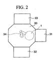
- the equipment having the configuration in which two CVD chambers 31, 32 are connected to a transfer chamber 30 whose pressure is lowered is employed.
- the silicon substrate 1 is transferred into the first CVD chamber 31 via a load lock chamber 33 and the transfer chamber 30, and then the first and second underlying layers 9, 10 are formed in the trench 8 and on the second interlayer insulating film 6 in the first CVD chamber 31.
- the silicon substrate 1 is transferred from the first CVD chamber 31 to the second CVD chamber 32 via the transfer chamber 30, and then the copper seed layer 11 is grown in the second CVD chamber 32.
- the silicon substrate 1 is taken out to the outside via the transfer chamber 30 and the load lock chamber 33.
- the transfer of the semiconductor substrate (wafer) 1 is executed by a robot arm 35.
- a pressure in the transfer chamber 30 is lowered, but such pressure is higher than pressures in the first and second CVD chambers 31, 32. Therefore, if the first and second underlying layers 9, 10 are grown in the first CVD chamber 31, penetration of the impurity between these underlying layers 9, 10 can be prevented, and thus reduction in the adhesion between the first and second underlying layers 9, 10 can be prevented and also increase in the resistance of the overall underlying layers can be prevented.
- such wiring 13 is covered with a silicon nitride film 7, and then the silicon nitride film 7 is covered with a third interlayer insulating film 14.
- the third interlayer insulating film 14 is formed at the growth temperature of the film forming temperature 300 to 450 °C by the CVD method using silane (SiH 4 ) and nitrogen monoxide (N 2 O).
- an intermediate layer 10a containing copper-zirconium alloy is formed between the copper layer 12 and the zirconium nitride layer constituting the second underlying layer 10 by the heating applied to form the third interlayer insulating film 14 or the heating applied to form the copper seed layer 11. Since the solid solubility of the zirconium to the copper is 0.02 %, the specific resistance of the intermediate layer 10a is substantially identical to the copper and the intermediate layer 10a is very thin.
- FIG.3(a) to FIG.3(c) various samples shown in FIG.3(a) to FIG.3(c) were formed and then experiments were executed. These samples are the sample shown in FIG.3(a) in which the first underlying layer 9 made of titanium nitride and having a film thickness of 10 nm and the second underlying layer 10 made of zirconium nitride and having a film thickness of 2.5 to 10.0 nm are grown sequentially on the SiO 2 film 15 by virtue of the CVD method respectively, the sample shown in FIG.3(b) in which the copper seed layer 11 having a thickness of 50 nm is grown on the second underlying layer 10, and the sample shown in FIG.3(c) in which the copper film 12 having a thickness of about 500 nm is grown on the copper seed layer 11 by the electrolytic plating method.
- the second underlying layer 10 may be formed like an island.
- the specific resistance of the overall underlying layers was reduced lower than 250 ⁇ ⁇ cm. Since the underlying layers 9, 10 function as the wiring 13, their specific resistance must be reduced smaller than 200 ⁇ ⁇ cm. For this reason, if the thickness of the titanium nitride film as the first underlying layer 9 is set to 10 nm, the thickness of the zirconium nitride film as the second underlying layer 10 must be set to 5 nm or less. That is, it is preferable that the film thickness of the zirconium nitride film should be set to smaller than 50 % of the film thickness of the titanium nitride film.
- the specific resistance of the titanium nitride constituting the first underlying layer 9 is 500 to 600 ⁇ ⁇ cm
- the specific resistance of the zirconium nitride constituting the second underlying layer 10 is 13.6 ⁇ ⁇ cm. Therefore, theoretically the specific resistance of the overall underlying layers is increased as the film thickness of the second underlying layer 10 is reduced. However, according to the experiments made by the inventors of this application, as shown in FIG.4, the specific resistance of the overall underlying layers was lowered as the film thickness of the second underlying layer 10 was reduced.
- the test indicating good or bad of the adhesion between the layers was decided depending on whether or not the copper film containing the copper seed layer is peeled off from the underlying layer when the adhesive tape that is posted on the copper film is peeled off forcedly. It was decided that the adhesion is good when such copper film is not peeled off from the underlying layer, while the adhesion is bad when such copper film is peeled off from the underlying layer.
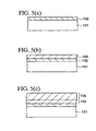
- FIG.5(a) shows the sample in which an underlying layer (barrier layer) 101 made of titanium nitride and having a film thickness of 15 nm is formed on an SiO 2 film 100
- FIG.5(b) shows the sample in which a copper seed layer 102 of 50 nm thickness is formed on the underlying layer 101
- FIG.5(c) shows the sample in which a copper layer 103 of about 500 nm thickness is formed on the copper seed layer 102.
- the specific resistance of the underlying layer 101 in FIG.5(a) is about 600 ⁇ ⁇ cm, and is 2.5 times or more rather than the specific resistances of the underlying layers 9, 10 having the structure shown in FIG.3(a) in the present embodiment.
- FIG.6 to FIG.8 are sectional views showing steps of forming a multi-layered copper wiring structure showing a second embodiment of the present invention.
- the same symbols as those shown in FIG.1(a) denote the same elements.
- the MOS transistor 3 formed on the silicon substrate 1 is covered with the first and second interlayer insulating films 4, 6, then the first wiring 13 is formed in the second interlayer insulating film 6, and then the silicon nitride film 7 and the third interlayer insulating film 14 are formed on the first wiring 13.
- a via hole 14a is formed in areas of the third interlayer insulating film 14 and the silicon nitride film 7, which overlap with the first wiring 13, by the photolithography method. Then, a trench 14b that passes over the via hole 14a is formed in an upper portion of the third interlayer insulating film 14 by the photolithography method.
- the via hole 14a is formed to have a depth that reaches the first wiring 13.
- the trench 14b is formed shallower than the via hole 14a by controlling the etching conditions of the third interlayer insulating film 14. Also, the trench 14b may be formed prior to the via hole 14a.
- a first underlying layer 16 made of TiN or TiN compound is formed on respective inner peripheral surfaces and bottom surfaces of the via hole 14a and the trench 14b and an upper surface of the third interlayer insulating film 14 to have a thickness of 5 to 10 nm.
- the TiN or TiN compound is grown by the CVD method using TDEAT under the same conditions as the first embodiment.
- a tantalum nitride (TaN) layer, a tungsten nitride (WN) layer may be formed as the first underlying layer 16 by the PVD method or the CVD method.
- a second underlying layer 17 made of ZrN or ZrN compound is formed in the same CVD chamber to have a thickness of 1 to 5 nm.
- the ZrN or ZrN compound is grown by the CVD method using TDEAZ under the same conditions as the first embodiment.
- a minute amount of NH 3 as well as the material gas may be supplied to the growth atmosphere (chamber).
- the growth conditions such as a flow rate of the gas, etc. pressure, temperature are controlled such that a ratio of the atomic number of the Zr in the second underlying layer 17 is in excess of 30 atoms%.
- the ZrN constituting the second underlying layer 17 has an average particle diameter of 10 nm or less, and the third underlying layer 17 is formed like a micro crystallite or an amorphous.
- a copper seed layer 18 of 30 to 100 nm thickness is formed on the second underlying layer 17 by the CVD method employing the material gas containing Cu(hfac)tmvs under the same conditions as the first embodiment, for example.
- a second copper layer 19 is formed on the copper seed layer 18 by the electrolytic plating to bury perfectly the via hole 14a and the second trench 14b.
- the second copper layer 19, the copper seed layer 18, and the first and second underlying layers 16, 17, which are formed on an upper surface of the third interlayer insulating film 14, are removed by the CMP method.
- the second copper layer 19, the copper seed layer 18, and the first and second underlying layers 16, 17, which are left in the via hole 14a are used as a conductive via 20, and also the second copper layer 19, the copper seed layer 18, and the first and second underlying layers 16, 17, which are left in the second trench 14b, are used as a second wiring 21.
- the first and second underlying layers 16, 17 act as lower layers of the via 20 and the wiring 21.
- the copper seed layer 18 and the second copper layer 19 act as main conductive layers of the via 20 and the wiring 21.
- a silicon nitride film, an interlayer insulating film, etc. (not shown) are formed on the second wiring 21.
- An alloy of zirconium and copper is formed between the second underlying layer and the copper layer 19 by the growth temperature applied when such insulating film is formed by the CVD method.
- the coverage of the underlying layer in the via hole 14a between the present embodiment and the prior art will be compared as follows.
- a TiN layer 110 was grown as the underlying layer in the via hole 14a and its periphery by the sputtering method. At this time, it was confirmed that such TiN layer 110 is overhung at the upper portion of the via hole 14a whereas the coverage at a lower side wall 14c of the via hole 14a is 10 % or less and is not good. The percentage of this coverage is a thickness of the film formed on the inner peripheral surface of the via hole 14a with respect to the diameter of the via hole 14a.
- a TiN layer 111 was grown as the underlying layer in the via hole 14a and its periphery by the CVD method employing TDEAT only. At this time, such TiN layer 111 was not overhung at the upper portion of the via hole 14a whereas the coverage at the lower side wall 14c of the via hole 14a was about 50 % or less. However, the specific resistance of the TiN layer 111 becomes high such as 500 ⁇ ⁇ cm or more.
- a TiN layer 112 was grown as the underlying layer in the via hole 14a and its periphery by the CVD method employing TDEAT, into which NH 3 is added, as the source gas. At this time, the specific resistance could be reduced up to about 200 ⁇ ⁇ cm. However, as shown in FIG.9(c), the coverage at the side wall of the via hole 14a became worse and thus the merit obtained by employing the CVD method is not exhibited. This is because TDEAT and NH 3 react with each other before they enter into the bottom of the via hole 14a.
- the underlying layers 16, 17 having the double-layered structure were formed by growing the TiN layer (the first underlying layer 16) in the via hole 14a and its periphery by the CVD method employing TDEAT and then growing the ZrN layer (the second underlying layer 17) by the CVD method employing TDEAZ.
- such TiN layer was not overhung at the upper portion of the via hole 14a, and the coverage at the lower side wall of the via hole 14a was about 50 %.
- the resistance ratio of the overall underlying layers 16, 17 could be reduced to 200 ⁇ ⁇ cm and thus the contact resistance between the via 20 and the first wiring 13 could be reduced.
- the zirconium nitride layer is formed in the via hole and the trench as the second underlying layer that is formed on the first underlying layer serving as the barrier layer to prevent the diffusion of copper. But that may be formed of other material.
- the material of the second underlying layer should have three properties such that such material is melted appropriately together the copper, the film resistance is relatively low, and such material can be grown by the CVD method.
- the constituent material of the second underlying layer has the appropriate solid solubility to the copper, the adhesion between the underlying layer and the copper layer can be improved.
- the film resistance is low, increase in the wiring resistance or the contact resistance can be suppressed and thus the merit obtained by forming the wiring resistance or the plug contact resistance of the copper can be used practically.
- the coverage in the via hole can be improved.
- cadmium (Cd), zinc (Zn), or silver (Ag) may be listed in addition to zirconium. Physical property values of these materials are given in Table 1. Resistance of Each Material and Solubility Limit to Cu Element Atomic Weight Specific Resistance( ⁇ ⁇ cm) Solubility Limit to Cu (wt%) Zr 91.224 40.00 0.02 Cd 112.411 6.83 4.0 Zn 65.390 5.92 40.0 Ag 107.868 1.59 >50.0
- Zn and Ag have the relatively large solubility limit to Cu.
- the resistance and Cu are alloyed when any one of these materials is used as the underlying layer, such material never increases largely the resistance of the copper layer.
- such material can be employed as the second underlying layer.
- Relationships between the specific resistance of the copper layer and an additive concentration when Zn, Zr, Cd, Ag, Si, Co, or Fe is added into the copper layer, which is formed on the underlying layer, as the additive are given as shown in FIG.11. According to FIG.11, because the addition of Si, Co or Fe to the copper layer causes an increase in the resistance of the copper layer, such addition is not preferable. In contrast, even if Zn, Zr, Cd or Ag is added to the copper layer, the resistance value of the copper layer is seldom changed.
- the specific resistance of the copper layer is about 2.20 ⁇ ⁇ cm if Ag is added to the copper layer by 10 wt%, while the specific resistance of the copper layer is about 2.10 ⁇ ⁇ cm if Zn is added to the copper layer by 10 wt%. Also, the resistance of the copper layer is 1.98 ⁇ ⁇ cm if Cd is added to the copper layer by 4 wt% as the solubility limit. In addition, the resistance of the copper layer is scarcely changed like about 1.69 ⁇ ⁇ cm if Zr is added to the copper layer by 0.02 wt% as the solubility limit.
- the metal constituting the second underlying layer should be solid-solved in the ranged of 0.01 to 10.0 wt% with respect to the copper.
- Zn, Cd, or Ag constituting the second underlying layer can be formed by the CVD method employing the source shown in Table 2.
- the metal deposited as the second underlying layer may be nitrided by employing ammonium (NH 3 ) or hydrazine (N 2 H 4 ) together with the material shown in Table 2 by several to several tens wt%.
- CVD Film Forming Material of Each Metal Deposited Metal CVD Material Cd(CH 3 ) 2 Dimethylcadmium Cd CdCl 2 Cadmium(II)chloride CdBr 2 Cadmium bromide Zn Zn(CH 3 ) 2 Dimethylzinc Zn(C 2 H 5 ) 2 Diethylzince Ag AgCl Silver chloride
- TDEAZ is employed when ZrN is formed as the second underlying layer by the CVD method.
- zirconium chloride ZrCl 4
- ZrCl 4 zirconium chloride
- an amount of impurity such as carbon, hydrogen, or the like can be reduced rather than the case that TDEAZ is employed.
- the ZrN layer is formed by employing ZrCl 4
- ammonium or hydrazine is added to ZrCl 4 by several or several tens wt%. In this case, if the Zr layer is formed as the second underlying layer, ammonium or hydrazine is not employed as the additive gas.
- the resistance of the second underlying layer that is formed by using ZrCl 4 is increased rather than the second underlying layer that is obtained from the TDEAZ material.
- the first underlying layer employed to prevent the diffusion of copper is grown by using the organic material, it is not preferable from a viewpoint of preventing the mixture of the carbon, etc. that the same CVD chamber should be employed.
- the SiO 2 layer containing the impurity such as fluorine, boron, or phosphorus may be employed as the material constituting the interlayer insulating film.
- the first underlying layer made of copper diffusion preventing conductive material such as titanium nitride, tantalum nitride, or tungsten nitride or material that contains them as major components, or the like;
- the second underlying layer formed on the first underlying layer and made of the material containing zirconium, cadmium, zinc or silver, or alloy of zirconium, cadmium, zinc or silver, or zirconium and nitrogen; and the main conductive layer formed on the second underlying layer and made of copper or copper alloy are buried in the insulating film as the wiring or the plug (via).
- the specific resistances of the first and second underlying layers are lowered rather than the case that the lower layer of the wiring or the plug is constructed only by the first underlying layer.
- the adhesion between these underlying layers and the copper layer or the copper alloy layer can be increased rather than the prior art.
- the good wiring or via can be constructed by the underlying layers and the copper layer or the underlying layers and the copper alloy layer.
Landscapes
- Internal Circuitry In Semiconductor Integrated Circuit Devices (AREA)
Abstract
Description
| Resistance of Each Material and Solubility Limit to Cu | |||
| Element | Atomic Weight | Specific Resistance(µ Ωcm) | Solubility Limit to Cu (wt%) |
| Zr | 91.224 | 40.00 | 0.02 |
| Cd | 112.411 | 6.83 | 4.0 |
| Zn | 65.390 | 5.92 | 40.0 |
| Ag | 107.868 | 1.59 | >50.0 |
| CVD Film Forming Material of Each Metal | ||
| Deposited Metal | CVD Material | |
| Cd(CH3)2 | Dimethylcadmium | |
| Cd | CdCl2 | Cadmium(II)chloride |
| CdBr2 | Cadmium bromide | |
| Zn | Zn(CH3)2 | Dimethylzinc |
| Zn(C2H5)2 | Diethylzince | |
| Ag | AgCl | Silver chloride |
Claims (19)
- A semiconductor device comprising:an insulating film formed over a semiconductor substrate;a trench and a hole formed in the insulating film;a first underlying layer formed in at least one of the trench and the hole and made of conductive material to prevent diffusion of copper;a main conductive layer formed in at least one of the trench and the hole on the first underlying layer and made of copper or copper alloy; anda second underlying layer formed between the main conductive layer and the first underlying layer and having a metal element that is solid-solved in the main conductive layer at an interface between the second underlying layer and the main conductive layer, and formed on the first underlying layer by a CVD method.
- A semiconductor device according to claim 1, wherein the second underlying layer is solid-solved in a range of 0.01 to 10.1 wt% with respect to the main conductive layer made of copper.
- A semiconductor device according to claim 1, wherein the second underlying layer is made of zirconium, cadmium, zinc or silver, or alloy of zirconium, cadmium, zinc or silver, or material containing zirconium and nitrogen.
- A semiconductor device according to claim 3, wherein the material containing zirconium and nitrogen is amorphous or microcrystalline zirconium nitride.
- A semiconductor device according to claim 3 or claim 4, wherein an average particle diameter of the material containing zirconium and nitrogen is 10 nm or less.
- A semiconductor device according to any one of claim 3 to claim 5, wherein the material containing zirconium and nitrogen contains the zirconium in excess of 30 atoms% of a ratio of number of atoms.
- A semiconductor device according to any one of claim 1 to claim 6, wherein the second underlying layer has a thickness of 5 nm or less.
- A semiconductor device according to any one of claim 1 to claim 7, wherein the second underlying layer has a film thickness that is smaller than half of the first underlying layer.
- A semiconductor device according to any one of claim 1 to claim 8, wherein the first underlying layer is made of any one of titanium nitride, tantalum nitride, and tungsten nitride.
- A semiconductor device according to any one of claim 1 to claim 9, wherein the first underlying layer has a thickness of 10 nm or less.
- A semiconductor device manufacturing method comprising the steps of:forming an insulating film over a semiconductor substrate;forming a trench and a hole in the insulating film;forming a first underlying layer, which is made of conductive material to prevent diffusion of copper, in the trench or the hole and on the insulating film by a CVD method;forming a second underlying layer, which has a metal element that is solid-solved in a copper layer, on the first underlying layer by the CVD method;forming a main conductive layer, which is made of copper or copper alloy, on the second underlying layer; andremoving the first underlying layer, the second underlying layer, and the main conductive layer from an upper surface of the insulating film to leave in the trench and the hole.
- A semiconductor device manufacturing method according to claim 11, wherein the second underlying layer is made of zirconium, cadmium, zinc or silver, or alloy of zirconium, cadmium, zinc or silver, or material containing zirconium and nitrogen.
- A semiconductor device manufacturing method according to claim 11, wherein the second underlying layer is made of a layer that contains zirconium and nitrogen, and is grown by using tetrakis(diethylamino)zirconium.
- A semiconductor device manufacturing method according to claim 11, wherein the second underlying layer is made of a layer that contains zirconium and nitrogen, and is grown by using zirconium chloride and a nitrogen compound gas.
- A semiconductor device manufacturing method according to any one of claim 11 to claim 14, wherein the second underlying layer has a thickness of 5 nm or less.
- A semiconductor device manufacturing method according to any one of claim 11 to claim 15, wherein the first underlying layer is made of any one of titanium nitride, tantalum nitride, and tungsten nitride.
- A semiconductor device manufacturing method according to any one of claim 11 to claim 15, wherein the first underlying layer is formed to have a thickness of 10 nm or less.
- A semiconductor device manufacturing method according to any one of claim 11 to claim 17, wherein the main conductor layer is formed by the step of forming a copper seed layer on a surface of the second underlying layer and then forming material containing copper as a major component or copper on the copper seed layer by a plating method.
- A semiconductor device manufacturing method according to any one of claim 11 to claim 18, wherein the first underlying layer, the second underlying layer, and the main conductive layer are removed from an upper surface of the insulating film to leave only in the trench and the hole.
Applications Claiming Priority (3)
| Application Number | Priority Date | Filing Date | Title |
|---|---|---|---|
| JP2000335690 | 2000-11-02 | ||
| JP2000335690 | 2000-11-02 | ||
| PCT/JP2001/009588 WO2002037558A1 (en) | 2000-11-02 | 2001-11-01 | Semiconductor device and its manufacturing method |
Publications (2)
| Publication Number | Publication Date |
|---|---|
| EP1331664A1 true EP1331664A1 (en) | 2003-07-30 |
| EP1331664A4 EP1331664A4 (en) | 2008-10-08 |
Family
ID=18811388
Family Applications (1)
| Application Number | Title | Priority Date | Filing Date |
|---|---|---|---|
| EP01980950A Withdrawn EP1331664A4 (en) | 2000-11-02 | 2001-11-01 | SEMICONDUCTOR DEVICE AND METHOD FOR MANUFACTURING THE SAME |
Country Status (7)
| Country | Link |
|---|---|
| US (1) | US6900542B2 (en) |
| EP (1) | EP1331664A4 (en) |
| JP (1) | JPWO2002037558A1 (en) |
| KR (1) | KR100769634B1 (en) |
| CN (1) | CN100334709C (en) |
| TW (1) | TW544789B (en) |
| WO (1) | WO2002037558A1 (en) |
Cited By (1)
| Publication number | Priority date | Publication date | Assignee | Title |
|---|---|---|---|---|
| CN101115864B (en) * | 2005-02-10 | 2010-10-13 | 东京毅力科创株式会社 | Thin film laminated structure, method for forming the same, film forming apparatus, and storage medium |
Families Citing this family (5)
| Publication number | Priority date | Publication date | Assignee | Title |
|---|---|---|---|---|
| JP2006249580A (en) * | 2005-02-10 | 2006-09-21 | Tokyo Electron Ltd | Thin film laminated structure, method for forming the same, film forming apparatus, and storage medium |
| JP4589787B2 (en) * | 2005-04-04 | 2010-12-01 | パナソニック株式会社 | Semiconductor device |
| WO2007094044A1 (en) * | 2006-02-14 | 2007-08-23 | Fujitsu Limited | Semiconductor device manufacturing method and semiconductor manufacturing apparatus |
| US7750852B2 (en) * | 2007-04-13 | 2010-07-06 | Semiconductor Energy Laboratory Co., Ltd. | Semiconductor device |
| US8105937B2 (en) * | 2008-08-13 | 2012-01-31 | International Business Machines Corporation | Conformal adhesion promoter liner for metal interconnects |
Family Cites Families (17)
| Publication number | Priority date | Publication date | Assignee | Title |
|---|---|---|---|---|
| DE3782904T2 (en) * | 1986-09-17 | 1993-04-08 | Fujitsu Ltd | METHOD FOR FORMING A METALIZING LAYER CONTAINING COPPER ON THE SURFACE OF A SEMICONDUCTOR COMPONENT. |
| US5288563A (en) | 1991-02-18 | 1994-02-22 | Japan Storage Battery Co., Ltd. | Hydrogen ion concentration sensor and lead-acid battery having the sensor |
| JPH05102152A (en) * | 1991-10-11 | 1993-04-23 | Sony Corp | Semiconductor device |
| JPH09330647A (en) * | 1996-06-07 | 1997-12-22 | Canon Inc | Electron-emitting device, electron source using the electron-emitting device, image forming apparatus using the electron source, and method for manufacturing the electron-emitting device |
| US5856236A (en) * | 1996-06-14 | 1999-01-05 | Micron Technology, Inc. | Method of depositing a smooth conformal aluminum film on a refractory metal nitride layer |
| KR100226764B1 (en) * | 1996-08-21 | 1999-10-15 | 김영환 | Thin film forming method using chemical vapor deposition system |
| US6130161A (en) * | 1997-05-30 | 2000-10-10 | International Business Machines Corporation | Method of forming copper interconnections with enhanced electromigration resistance and reduced defect sensitivity |
| US6069068A (en) * | 1997-05-30 | 2000-05-30 | International Business Machines Corporation | Sub-quarter-micron copper interconnections with improved electromigration resistance and reduced defect sensitivity |
| US6022808A (en) | 1998-03-16 | 2000-02-08 | Advanced Micro Devices, Inc. | Copper interconnect methodology for enhanced electromigration resistance |
| US6461675B2 (en) | 1998-07-10 | 2002-10-08 | Cvc Products, Inc. | Method for forming a copper film on a substrate |
| JP4248649B2 (en) | 1998-12-18 | 2009-04-02 | 株式会社エンプラス | Socket for electrical parts |
| US6265779B1 (en) * | 1998-08-11 | 2001-07-24 | International Business Machines Corporation | Method and material for integration of fuorine-containing low-k dielectrics |
| JP2000183003A (en) | 1998-10-07 | 2000-06-30 | Toshiba Corp | Polishing composition for copper-based metal and method for manufacturing semiconductor device |
| JP2001015517A (en) * | 1999-07-02 | 2001-01-19 | Ebara Corp | Semiconductor device and its manufacture |
| KR100361207B1 (en) * | 1999-12-29 | 2002-11-18 | 주식회사 하이닉스반도체 | A method of forming a metal line in a semiconductor device |
| JP4733804B2 (en) * | 2000-02-18 | 2011-07-27 | 富士通セミコンダクター株式会社 | Wiring formation method |
| JP4005295B2 (en) * | 2000-03-31 | 2007-11-07 | 富士通株式会社 | Manufacturing method of semiconductor device |
-
2001
- 2001-11-01 KR KR1020037005134A patent/KR100769634B1/en not_active Expired - Fee Related
- 2001-11-01 CN CNB018179967A patent/CN100334709C/en not_active Expired - Fee Related
- 2001-11-01 WO PCT/JP2001/009588 patent/WO2002037558A1/en not_active Ceased
- 2001-11-01 EP EP01980950A patent/EP1331664A4/en not_active Withdrawn
- 2001-11-01 TW TW090127183A patent/TW544789B/en not_active IP Right Cessation
- 2001-11-01 JP JP2002540208A patent/JPWO2002037558A1/en active Pending
-
2003
- 2003-05-02 US US10/428,208 patent/US6900542B2/en not_active Expired - Lifetime
Cited By (1)
| Publication number | Priority date | Publication date | Assignee | Title |
|---|---|---|---|---|
| CN101115864B (en) * | 2005-02-10 | 2010-10-13 | 东京毅力科创株式会社 | Thin film laminated structure, method for forming the same, film forming apparatus, and storage medium |
Also Published As
| Publication number | Publication date |
|---|---|
| WO2002037558A1 (en) | 2002-05-10 |
| JPWO2002037558A1 (en) | 2004-03-11 |
| TW544789B (en) | 2003-08-01 |
| CN100334709C (en) | 2007-08-29 |
| CN1633708A (en) | 2005-06-29 |
| US6900542B2 (en) | 2005-05-31 |
| EP1331664A4 (en) | 2008-10-08 |
| KR20030060908A (en) | 2003-07-16 |
| US20040000716A1 (en) | 2004-01-01 |
| KR100769634B1 (en) | 2007-10-23 |
Similar Documents
| Publication | Publication Date | Title |
|---|---|---|
| CN101504932B (en) | Semiconductor device and manufacturing method | |
| US5939788A (en) | Copper diffusion barrier, aluminum wetting layer and improved methods for filling openings in silicon substrates with cooper | |
| US8071474B2 (en) | Method of manufacturing semiconductor device suitable for forming wiring using damascene method | |
| US7154178B2 (en) | Multilayer diffusion barrier for copper interconnections | |
| US6229211B1 (en) | Semiconductor device and method of manufacturing the same | |
| US6294836B1 (en) | Semiconductor chip interconnect barrier material and fabrication method | |
| US6977220B2 (en) | Copper alloys for interconnections having improved electromigration characteristics and methods of making same | |
| KR0179822B1 (en) | Interconnections structure of semiconductor device and method for manufacturing thereof | |
| US9559058B2 (en) | Semiconductor device and method for manufacturing the same | |
| US8106512B2 (en) | Low resistance high reliability contact via and metal line structure for semiconductor device | |
| US20080242088A1 (en) | Method of forming low resistivity copper film structures | |
| US9704740B2 (en) | Semiconductor device having insulating layers containing oxygen and a barrier layer containing manganese | |
| US6998342B2 (en) | Electronic device manufacturing method | |
| JP2009231497A (en) | Semiconductor device and manufacturing method therefor | |
| US5994775A (en) | Metal-filled via/contact opening with thin barrier layers in integrated circuit structure for fast response, and process for making same | |
| JPH11150087A (en) | Method of forming titanium nitride barrier layer and semiconductor device including titanium nitride barrier layer | |
| US6569756B1 (en) | Method for manufacturing a semiconductor device | |
| US6900542B2 (en) | Semiconductor device having increased adhesion between a barrier layer for preventing copper diffusion and a conductive layer, and method of manufacturing the same | |
| JPS63172463A (en) | Semiconductor device | |
| KR101088813B1 (en) | Metal wiring of semiconductor device and method of forming the same | |
| US20070052098A1 (en) | Metal line for a semiconductor device and fabrication method thereof |
Legal Events
| Date | Code | Title | Description |
|---|---|---|---|
| PUAI | Public reference made under article 153(3) epc to a published international application that has entered the european phase |
Free format text: ORIGINAL CODE: 0009012 |
|
| 17P | Request for examination filed |
Effective date: 20030424 |
|
| AK | Designated contracting states |
Designated state(s): DE FR GB IT |
|
| A4 | Supplementary search report drawn up and despatched |
Effective date: 20080904 |
|
| RAP1 | Party data changed (applicant data changed or rights of an application transferred) |
Owner name: FUJITSU MICROELECTRONICS LIMITED |
|
| 17Q | First examination report despatched |
Effective date: 20091120 |
|
| RAP1 | Party data changed (applicant data changed or rights of an application transferred) |
Owner name: FUJITSU SEMICONDUCTOR LIMITED |
|
| GRAP | Despatch of communication of intention to grant a patent |
Free format text: ORIGINAL CODE: EPIDOSNIGR1 |
|
| RAP1 | Party data changed (applicant data changed or rights of an application transferred) |
Owner name: FUJITSU SEMICONDUCTOR LIMITED |
|
| RIC1 | Information provided on ipc code assigned before grant |
Ipc: H01L 23/532 20060101ALI20161010BHEP Ipc: H01L 21/768 20060101AFI20161010BHEP |
|
| INTG | Intention to grant announced |
Effective date: 20161103 |
|
| RIN1 | Information on inventor provided before grant (corrected) |
Inventor name: OHTSUKA, NOBUYUKI Inventor name: SAKAI, HISAYA Inventor name: SHIMIZU, NORIYOSHI |
|
| STAA | Information on the status of an ep patent application or granted ep patent |
Free format text: STATUS: THE APPLICATION IS DEEMED TO BE WITHDRAWN |
|
| 18D | Application deemed to be withdrawn |
Effective date: 20170314 |