EP1330852B1 - Rundstrahlende antenne mit mehreren polarisationen - Google Patents
Rundstrahlende antenne mit mehreren polarisationen Download PDFInfo
- Publication number
- EP1330852B1 EP1330852B1 EP01975471A EP01975471A EP1330852B1 EP 1330852 B1 EP1330852 B1 EP 1330852B1 EP 01975471 A EP01975471 A EP 01975471A EP 01975471 A EP01975471 A EP 01975471A EP 1330852 B1 EP1330852 B1 EP 1330852B1
- Authority
- EP
- European Patent Office
- Prior art keywords
- antenna assembly
- conductive
- loop element
- antenna
- ground plane
- Prior art date
- Legal status (The legal status is an assumption and is not a legal conclusion. Google has not performed a legal analysis and makes no representation as to the accuracy of the status listed.)
- Expired - Lifetime
Links
Images


Classifications
-
- H—ELECTRICITY
- H01—ELECTRIC ELEMENTS
- H01Q—ANTENNAS, i.e. RADIO AERIALS
- H01Q1/00—Details of, or arrangements associated with, antennas
- H01Q1/36—Structural form of radiating elements, e.g. cone, spiral, umbrella; Particular materials used therewith
- H01Q1/38—Structural form of radiating elements, e.g. cone, spiral, umbrella; Particular materials used therewith formed by a conductive layer on an insulating support
-
- H—ELECTRICITY
- H01—ELECTRIC ELEMENTS
- H01Q—ANTENNAS, i.e. RADIO AERIALS
- H01Q1/00—Details of, or arrangements associated with, antennas
- H01Q1/12—Supports; Mounting means
- H01Q1/22—Supports; Mounting means by structural association with other equipment or articles
- H01Q1/24—Supports; Mounting means by structural association with other equipment or articles with receiving set
- H01Q1/241—Supports; Mounting means by structural association with other equipment or articles with receiving set used in mobile communications, e.g. GSM
- H01Q1/242—Supports; Mounting means by structural association with other equipment or articles with receiving set used in mobile communications, e.g. GSM specially adapted for hand-held use
- H01Q1/243—Supports; Mounting means by structural association with other equipment or articles with receiving set used in mobile communications, e.g. GSM specially adapted for hand-held use with built-in antennas
-
- H—ELECTRICITY
- H01—ELECTRIC ELEMENTS
- H01Q—ANTENNAS, i.e. RADIO AERIALS
- H01Q9/00—Electrically-short antennas having dimensions not more than twice the operating wavelength and consisting of conductive active radiating elements
- H01Q9/04—Resonant antennas
- H01Q9/0407—Substantially flat resonant element parallel to ground plane, e.g. patch antenna
- H01Q9/0421—Substantially flat resonant element parallel to ground plane, e.g. patch antenna with a shorting wall or a shorting pin at one end of the element
-
- H—ELECTRICITY
- H01—ELECTRIC ELEMENTS
- H01Q—ANTENNAS, i.e. RADIO AERIALS
- H01Q9/00—Electrically-short antennas having dimensions not more than twice the operating wavelength and consisting of conductive active radiating elements
- H01Q9/04—Resonant antennas
- H01Q9/0407—Substantially flat resonant element parallel to ground plane, e.g. patch antenna
- H01Q9/0442—Substantially flat resonant element parallel to ground plane, e.g. patch antenna with particular tuning means
-
- H—ELECTRICITY
- H01—ELECTRIC ELEMENTS
- H01Q—ANTENNAS, i.e. RADIO AERIALS
- H01Q9/00—Electrically-short antennas having dimensions not more than twice the operating wavelength and consisting of conductive active radiating elements
- H01Q9/04—Resonant antennas
- H01Q9/0407—Substantially flat resonant element parallel to ground plane, e.g. patch antenna
- H01Q9/0464—Annular ring patch
Definitions
- This invention relates generally to antenna structures for wireless communications devices, and more particularly to compact, high efficiency, electrically small loop antennas for use in conjunction with portable wireless communication devices.
- modem compact communication devices often is dictated by the size of the antenna needed to make them function effectively.
- pagers and other devices have made use of electrically small rectangular loop (1/10 wavelength).
- these small antennae tend to be inefficient as a result of their very low radiation resistance and comparatively high resistive loss.
- high Q they tend to be sensitive to their physical environment.
- modem wireless communications devices Yet another consideration and challenge of designing modem wireless communications devices is the efficiency of packaging the necessary components within an increasing smaller physical package.
- a particularly difficult challenge to those skilled in the relevant arts has been the efficient placement of components, such as batteries, antenna structures, RF signal reception and transmission circuits, and other digital and/or analog devices or module, within the overall device package.
- components such as batteries, antenna structures, RF signal reception and transmission circuits, and other digital and/or analog devices or module.
- antenna structures and assemblies relative to the RF signal generating components or modules.
- antennas small in physical dimension; having relatively high efficiency; capable of being placed in close proximity to associated electronic circuits without adversely effecting performance; easy to manufacture using standard, low-cost components; and capable of having radiation patterns altered to support different applications.
- an antenna assembly may be located remotely from the electronic device or devices it is serving. Remote location of the antenna assembly relative the associated wireless device may minimize coupling of RF energy into digital or other circuitry from the strong fields around the antenna or for the antenna to have access to signals.
- One limitation associated with a remote antenna is that power is lost through the transmission line connecting the antenna assembly to the electronics. Obviously, this is undesirable as it degrades the performance of the system by increasing the noise and reducing the transmit power. A decrease in important antenna parameters, such as gain, results from power loss in the transmission line. Signal reception is also negatively impacted by transmission line losses.
- Circular polarization antenna structures or systems for reception of left hand and right hand polarized signals are also known.
- Circular polarization is typical of satellite systems, such as the Global Positioning System (GPS). This field is in rapid expansion due to the vast range of possible applications and the relative low cost of implementing these systems.
- GPS Global Positioning System
- the fixed and mobile land devices associated with such systems have required more specialized antennas designed to perform specific functions effectively.
- Two types of antennas have to date been used in circular polarization communication and navigation systems on mobile devices: the first is the "helix” or helicoidal antenna, while the second is known as the "patch” antenna.
- circular polarization is obtained by exciting a progressive wave on a helicoidal wire; the direction of the circular polarization (left or right) is determined by the sense of helicoidal wire winding.
- the helicoidal antennas have the advantage of being very simple to design and produce and have a considerable band width which ensures high sensitivity; this characteristic of the helicoidal antenna makes the tolerance range wider, making it possible to use inexpensive materials which are easy to obtain on the market.
- This type of antenna has the added advantage of having a good gain value in an axial direction with an equally good axial ratio that, as the experts in the field know, is the most important reference parameter for the quality of circular polarization.
- helicoidal antennas are their by no means negligible height which makes them inconvenient for certain applications, such as installation on vehicles or handheld devices where low profile antennas are required, obviously because they must be streamlined.
- the low profile is the main characteristic of the second type of antenna mentioned above, known as the patch antenna, where circular polarization is obtained by exciting a resonant current distribution on a planar conducting surface.
- the direction of circular polarization is determined by a precise calculation of the position of the "point of excitation" of the surface.
- This type of antenna requires the use of relatively expensive materials, and, above all great precision during setting up and production due to the small tolerances to respect.
- GB 2,289,163 discloses an antenna device comprising an electrically conductive closed loop spaced above a ground plane, with two connection points spaced around the loop for connection to a radio frequency transmitter or receiver.
- the circumference of the loop may be between 1-half and three quarters of the desired signal wavelength, whilst the circumference of the loop is typically set at about five-eights of the wavelength or less.
- the shape of the loop is preferably circular, but other shapes such as squares, hexagons, triangles may be employed.
- US 5, 945, 959 discloses an antenna device including a dielectric base body having an upper face and a lower face in parallel with each other, a radiating conductor film formed on the upper face of the dielectric base body, having two ends adjacent to each other in connecting the two ends in a loop-like shape, and a grounding conductor film formed on the lower face of the dielectric base body and extending in a planar shape, wherein feeding conductor films are formed on a side face of the dielectric base body, respectively connected to the two ends of the radiating conductor film, extending in an up and down direction in parallel with each other, one of which is connected to the grounding conductor film.
- US 4, 924,237 discloses an antenna comprising a ground conductor plane, a radiating conductor plane disposed in parallel space relation to the ground plane and shorted at its one end to the ground plane.
- the ground plane is preferably formed on a printed board which is disposed in parallel relation to the radiating plane.
- An open air space is defined between the ground plane and radiating plane. No dielectric element is located between the ground plane and radiating plane.
- An omni-directional antenna which includes a conductive loop element supported above a conductive ground plane of a wireless communication device by a conductive leg member.
- the conductive leg member further defines a feedpoint at which the antenna is operatively coupled to the device's signal generating circuitry.
- a dielectric element may optionally be disposed between the loop and ground plane.
- the improved antenna displays gain in both the vertical and horizontal orientations.
- the horizontal gain is due to currents in the loop.
- the vertical gain (perpendicular to the loop and the ground plane) is due to displacement current fields within the conductive leg member disposed between the loop and the ground plane.
- Circular polarization is obtained by exciting a wave along a loop wire.
- the loop defines a closed path, which need not necessarily be a circular path.
- An antenna including a rectangularly defined loop is also disclosed herein.
- Different approaches may be utilized to effect wave polarization (left-hand or right-hand); the first consists in exciting the loop wire at two separate points staggered at an angle of 90 degrees with respect to the center of the loop wire and providing a source in phase quadrature.
- the loop wire may be excited at only one point by discriminating one of the two polarizations by means of a passive probe, a directional probe or other suitable means.
- the operational frequency band of the antenna is largely determined by the outside circumference dimension of the conductive loop.
- the outer circumference dimension is substantially equivalent to 1/2 of the wavelength of the frequency of response.
- Tuning of the antenna can be accomplished by adjusting the feed network. Adjusting the width and location of the conductive leg member will transition the frequency and impedance.
- LNA low noise amplifier
- a LNA with or without pre/post filter may be disposed within a cavity of a portion of the antenna assembly.
- the electronic or other components may be disposed within a cavity defined within a disk-shaped dielectric element.
- an antenna structure having a conductive loop resonator element disposed in operative relationship to a conductive ground plane element.
- the conductive ground plane may be the ground plane of a wireless communications device.
- the conductive ground plane may be a separate conductive panel or element which is coupled to the ground plane of the wireless device.
- the antenna may be remotely disposed relative to the wireless device and coupled thereto by a transmission line, such as a coax signal line, etc.
- Yet another feature of embodiments of the present invention is a notch element in the conductive leg member. Changes in the notch height can be used to adjust the antenna match. Further tuning can be accomplished by adjusting the width of the ring. As the ring is made wider, the operational frequency range becomes higher.
- One advantage of the invention is that the antenna performance is largely independent of the dimensions of the ground plane.
- the antenna can be readily adapted to different devices having various ground plane dimensions.
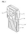
- FIG. 1 illustrates an antenna assembly 10 disposed within a wireless communications device 12, such as a cellular telephone or PDA device.
- the antenna assembly 10 includes a circular loop resonator element 14 defining a loop surface 16 disposed away from a ground plane element 20.
- the ground plane element 20 may be ground plane of a printed wiring board of the device 12 or may be a separate conductive element which is coupled to the ground plane of the device 12.
- the antenna assembly 12 can be implemented to transmit and receive on desired frequencies, including analog or digital U.S. or European cell phone bands, PCS cell phone bands, 2.4 GHz BLUETOOTH® bands, or other frequency bands as would be obvious to one skilled in the art.
- the antenna assembly 10 is disposed near the upper portion of the device 12 (away from the user's hand during operation), and is received and incorporated within the housing 22 of the device 12. Although the antenna assembly 10 can be installed in locations within or external to the housing 22, it is presently preferred that it be disposed within the housing 22.
- Wireless communication device 12 contains an electronic device, such as a receiver and/or transmitter herein referred for convenience together as a transceiver component 24.
- ground plane 20 is illustrated herein as a substantially rectangular form. It should be recognized that ground plane 20 may assume alternative shapes or forms, provided that at least one major dimension is approximately 1 ⁇ 4 wavelength long at the lowest frequency of operation.
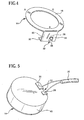
- a conductive leg element 26 is contiguous with and extends from an edge of the loop surface 16 toward the ground plane element and defines a feed tab 28 for the antenna assembly 12. The feed tab 28 is operatively coupled to the transceiver signal input/output component 24, such as via a coax line 25 of FIG. 5.
- the conductive leg element 26 further defines a ground tab 30 for coupling the leg element 26 to a circuit ground.
- Loop resonator 14 is thus electrically connected to the ground plane 20 via the ground tab 30.
- a slot-like removed portion 32 is defmed between the feed tab 28 and the ground tab 30 of the conductive leg element 26.
- the slot-like removed portion 32 is illustrated as a slot having generally parallel edges. Alternative embodiments of the slot-like removed portion 32 may be practicable, including but not limited to notch structures, or other removed portions.
- the dimensions of the loop resonator element 14 may be varied to conform to a portion of the housing 22. Those skilled in the arts will appreciate that the design and selection of the loop resonator element 14 with reference to a particular wireless communication device may result in such complex shapes.
- a disk-shaped dielectric element 40 is disposed between the conductive loop resonator element 14 and the ground plane 20.
- the dielectric element 40 may include a glass filled polymer such as ULTEM 1000 (available from Boedeker Plastics, Inc. of Shiner, TX) for the dielectric disk. This material is a glass filled polymer which has a dielectric constant of approximately 3.15. This dielectric material is suitable for the antenna 10 to be surface mounted through a thermal reflow solder process. Other dielectric materials can be used as well. Those skilled in the relevant art will appreciate that selection of a dielectric material having a higher dielectric constant can result in a smaller, more compact, antenna 10. Dielectric constant values are preferably in the range from 1 to 35.
- dielectric materials should include considerations including high temperature resistance, and low loss factor for antenna performance.
- Other dielectric materials which may be suitable include ceramic materials, and aerogels. Ceramic filled plastics can also be used, such as TMM material manufactured by Rogers Corporation, of Chandler, Arizona, which is available in dielectric constant values from 3 to 10, and which is resistant to solder reflow temperatures. TMM material consists of a hydrocarbon thermoset plastic (ceramic-filled) that provides a tight control of dielectric constant, low loss, and excellent temperature stability.
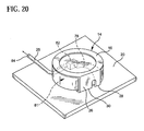
- the dielectric element 40 may include a cavity into which one or more components of the WCD 12 may be disposed. FIGS. 20 - 21 illustrate such an embodiment as further described herein.
- the conductive loop resonator element 14 and leg element 26 can be integrally manufactured from a single conductive metal or other suitable conductive material.
- the conductive metal would be 0.25 mm thick brass for operation about the 2.4-2.5 GHz frequency range.
- the conductive members 14, 26 can be shaped by stamping, milling, plating or other suitable method as would be obvious to one skilled in the relevant arts.
- the conductive members 14, 26 may also be overmolded with a polymeric dielectric 40, or mechanically secured onto the dielectric member 40.
- the conductive members 14, 26 may be selectively plated onto the dielectric member 40 using electrolytic or electroless or other suitable methods.
- One particular method would employ the MID technology of two shot molding followed by electroless plating.
- the manufacturing method may employ insert molding over the existing conductive portion.
- the loop resonator element 14 can be soldered onto the wiring board of the communication device 12 for electrical and mechanical coupling of the feed tab 28 to the signal transceiver component 24, and the ground tab 30 to the ground portion of the transceiver component 24.
- a microstrip feedline (not shown) from the communication device 12 to the antenna 10 can also be employed.
- a primary advantage of this invention is that multiple polarizations can be obtained from a very compact design.
- the unit produces right hand and left hand circular polarizations as well as vertical and horizontal responses.
- the right hand side of the antenna 10 transmits and receives right hand circular polarized radiation, while the left side of the antenna 10 transmits and receives left hand circular polarized radiation.
- the antenna 10 also transmits and receives vertical polarization in the azimuthal direction which is nearly perfectly omni-directional, and horizontal polarization at zenith.
- the antenna 10 is particularly well suited for GPS usage at 1.575 GHz due to the right hand circular polarization response.
- the antenna 10 can also be built scaled in size to perform in the BLUETOOTH® frequency band, at 2.4 GHz.
- This antenna 10 is also well suited for BLUETOOTH® and ISM applications since the multiple dimensions of polarization performance allow the unit to be oriented in many angles of configuration and still have good response.
- the antenna 10 can be used in a handheld device 12 which can be carried in any orientation and still provide acceptable signal transmission and reception quality.
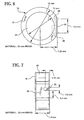
- the antenna 10 can be considered as a 1/2 wave loop antenna with an electrical distance around the ring of 1/2 wavelength at 2.45 GHz. Describing the antenna 10 in this manner leads to the definition of points about the ring corresponding to distances along the wavelength. In Figure 3 the 0, 1/4 and 1/2 wavepoints are indicated by A, B and C respectively.
- a current standing wave (CSW) is set up around the ring 16.
- a voltage standing wave (VSW), phase shifted 90°, is established between the ring 16 and the groundplane 20.
- the conduction current of the CSW produces a horizontally polarized E-field and the displacement current from the VSW produces a vertically polarized E-field.
- Circular polarization requires a 90° phase shift between polarizations, which is inherent in this design.
- the E-fields from the two polarizations must be equal in magnitude. This second requirement does not occur at any of the locations on the ring having either a current or a voltage null (0, 1/4 and 1/2 wave points).
- FIG. 9 illustrates the voltage standing wave ratio (VWSR) vs. frequency plot for the antenna of FIGS. 6-7.
- VWSR voltage standing wave ratio
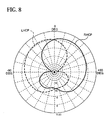
- the radiation pattern of this particular antenna is nearly omnidirectional for vertical polarization, in the plane which is parallel to the ground plane. In comparison, this radiation pattern is substantially different from a typical PIFA antenna pattern.
- Two dimensions on the antenna 10 can be adjusted to tune the antenna 10 into the desired operational band.
- material can be removed from the left side of the conductive leg element 26 and ground tab 30 as shown in FIG. 4 as phantom lines 60. Changes should be of the order of 0.25 mm to change the resonance frequency by 25 MHz. These numbers are not exact but do give an order of magnitude. This removal of the material makes the slot longer and thereby lowers the frequency.
- the slot between the leg element 26 and ground tab 30 and the feed tab 26 should be lengthened (as indicated by phantom line 70 in FIG. 4). Relatively minor changes of the order of 0.25 mm should be necessary.
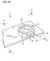
- FIGS. 10-12 illustrate another embodiment of an antenna assembly 10 for a wireless communications device 10.
- a conductive leg member 50 includes a feed point 52 defined a distance away from both the ground plane 20 of the device 12 and the ground tab 54 of the conductive leg member 50. Coupling to the device transceiver component 24 may be via a coax or other signal line.
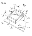
- FIGS. 13-18 illustrate yet another embodiment of an antenna assembly 10 for a wireless communications device 10.
- the loop resonator 14 and dielectric substrate element 40 of this embodiment are preferably rectangular in form, and yet more preferably substantially square in shape.
- FIGS. 14 -18 are additional views of the antenna of FIG. 13.
- the antenna of FIGS. 13-18 include a plurality of side conductor panels 70, 72, 74 electrically coupled to the loop resonator element 14 proximate its perimeter.
- a conductive leg member 60 includes a feed point 62 defined a distance away from both the ground plane 20 of the device 12 and the ground tab 64 of the conductive leg member 60.
- a 50 ohm unbalanced electrical feed point is provided between feed point 62 and ground tab 64.
- Coupling to the device transceiver component 24 may be via a coax or other signal line.
- the antenna 10 may be disposed away from the associated wireless communications device 12.
- the loop surface 16 of the circular loop resonator element 14 is disposed in substantially parallel relationship to the ground plane element 20 which may be a conductive element separate from the ground plane of the wireless device 12.
- ground plane 20 may assume alternative shapes or forms, provided that at least one major dimension is approximately 1 ⁇ 4 wavelength long at the lowest frequency of operation.
- a conductive leg element 26 is contiguous with and extends from an edge of the loop surface 16 toward the ground plane element and defines a feed tab 28 for the antenna assembly 12.
- the feed tab 28 is operatively coupled via a conductor 78 to the output 80 of a low noise amplifier 82 which is coupled to a transmission line, such as coax line 25.
- the shield conductor 84 of the coax line 25 is coupled to the ground plane 20 of the antenna assembly.
- a component such as a low noise amplifier 82, is disposed between in a region 81 between the conductive loop resonator element 14 and the ground plane 20.
- One or more components, such as circuits or other electronic devices or systems, may be disposed in such relationship, i.e., between the conductive loop resonator element 14 and the ground plane 20.
- the height of the component(s) or circuit(s) disposed between the loop resonator element 14 and the ground plane 20 should be less than approximately 50% of the distance between the loop resonator 14 and the ground plane 20.
- the conductive leg element 26 further defines a ground tab 30 for coupling the leg element 26 to the ground plane 20.
- Loop resonator 14 is thus electrically connected to the ground plane 20 via the ground tab 30.
- a slot 32 is defined between the feed tab 28 and the ground tab 30 of the conductive leg element 26.
- the dimensions of the loop resonator element 14 may be varied to conform to a portion of the housing 22. Those skilled in the arts will appreciate that the design and selection of the loop resonator element 14 with reference to a particular wireless communication device 12 may result in such complex shapes.
- a disk-shaped dielectric element 40 is disposed in the region 81 between the conductive loop resonator element 14 and the ground plane 20.
- the dielectric element 40 may include a glass filled polymer such as ULTEM 1000 (available from Boedeker Plastics, Inc. of Shiner, TX) for the dielectric disk. This material is a glass filled polymer which has a dielectric constant of approximately 3.15. This dielectric material is suitable for the antenna 10 to be surface mounted through a thermal reflow solder process. Other dielectric materials can be used as well. Those skilled in the relevant art will appreciate that selection of a dielectric material having a higher dielectric constant can result in a smaller, more compact, antenna 10.
- Dielectric constant values are preferably in the range from 1 to 35.
- the selection of dielectric materials should include considerations including high temperature resistance, and low loss factor for antenna performance.
- Other dielectric materials which may be suitable include ceramic materials, and aerogels. Ceramic filled plastics can also be used, such as TMM material manufactured by Rogers Corporation, of Chandler, Arizona, which is available in dielectric constant values from 3 to 10, and which is resistant to solder reflow temperatures.
- TMM material consists of a hydrocarbon thermoset plastic (ceramic-filled) that provides a tight control of dielectric constant, low loss, and excellent temperature stability.
- the dielectric element 40 may include a cavity 86 into which one or more components of the WCD 12, such as the low noise amplifier 82, may be disposed. One or more components of the wireless device 12 may be placed within the cavity or cavities 86 of a dielectric element 40.
- the feed structure 90 of FIG. 22 includes a pair of conductive wires 92, 94 coupled to the center conductor 83 and shield conductor 84 of coax line 25, respectively. Shield conductor 84 and conductive wire 94 are connected to the ground plane 20.
- the conductive wires 92, 94 may have circular cross sections with a diameter, D 2 .
- the conductive wires 92, 94 are disposed away from each other a distance, D 1 . Tuning of the feed structure 90 may be accomplished by varying the distances D 1 and D 2 .
- the feed structure 98 of FIG. 23 is a high impedance (voltage feed) structure which includes an inductor 100 and capacitor 102 coupled in parallel.
- the inductor 100 and capacitor 102 may be separate, discrete components, or may be incorporated within a LC tuning network.
- the center conductor 83 of a coax feed line 25 is coupled proximate to the inductor 100, and the shield conductor 84 is coupled to the ground plane 20.
- the feed structures 90, 98 of FIGS. 22 and 23 are illustrated to include a coax signal line 25.
- Alternative signal lines may also be practicable in alternative embodiments of the antenna, e.g., a micro-strip transmission line.
Claims (15)
- Antennenanordnung für ein Funkkommunikationsgerät (10), das auf einer vorab festgelegten Betriebswellenlänge arbeitet und eine Transceiver-Schaltung aufweist, die einen Signalanschluß und eine Masseplatte enthält, wobei die Antennenanordnung umfaßt:ein im allgemeinen planares leitfähiges Schleifenelement (14), wobei genanntes leitfähiges Schleifenelement in einem vorab festgelegten Abstand von der Masseplatte (20) weg und in allgemeiner paralleler Ausrichtung mit der Masseplatte (20) angeordnet ist, um ein Gebiet zwischen dem Schleifenelement (14) und der Masseplatte (20) zu definieren, wobei das Gebiet so dimensioniert ist, daß es eine zum Funkkommunikationsgerät zugehörige Komponente aufnimmt, undeine leitfähige Speisestruktur, die mit dem leitfähigen Schleifenelement (14) gekoppelt ist und in Richtung auf die Masseplatte (20) verläuft, wobei genannte leitfähige Speisestruktur eine Speisepunktverbindung und eine Masseverbindung aufweist, wobei die Anordnung ferner ein dielektrisches Element (40) aufweist, das in dem Gebiet zwischen dem leitfähigen Schleifenelement (14) und der Masseplatte (20) angeordnet ist, dadurch gekennzeichnet, daß das leitfähige Schleifenelement eine elektrische Länge von näherungsweise der halben vorab festgelegten Wellenlänge aufweist und das dielektrische Element (40) einen inneren Hohlraum zur Aufnahme einer zum Funkkommunikationsgerät zugehörigen Komponente enthält.
- Antennenanordnung nach Anspruch 1, dadurch gekennzeichnet, daß die Speisestruktur ein Schenkelteil (26) mit einem oberen und einem unteren Ende enthält, wobei genanntes oberes Ende mit dem Schleifenelement (14) gekoppelt ist, wobei genanntes unteres Ende mit der Masseplatte (20) an einer Masseverbindungsstelle und dem Signalausgang an einer Speisepunktstelle gekoppelt ist, wobei genanntes Schenkelteil (26) einen schlitzartigen entfernten Abschnitt (32) aufweist, der zwischen der Speisepunktstelle und der Masseverbindungsstelle definiert ist.
- Antennenanordnung nach Anspruch 2, dadurch gekennzeichnet, daß das leitfähige Schenkelteil (26) mit der Signalausgangverbindung an einer Speisepunktstelle gekoppelt ist, wobei genanntes Schenkelteil (26) einen schlitzartigen entfernten Abschnitt (32) aufweist, der zwischen der Speisepunktstelle und der Masseverbindungsstelle definiert ist.
- Antennenanordnung nach Anspruch 2 oder 3, dadurch gekennzeichnet, daß das leitfähige Schenkelteil (26) allgemein planar ist und eine Speisezunge (28) an der Speisepunktstelle und eine Massezunge (30) an der Masseverbindungsstelle enthält.
- Antennenanordnung nach einem der Ansprüche 2 bis 4, dadurch gekennzeichnet, daß das leitfähige Schleifenelement (14) und das leitfähige Schenkelteil (26) aus einem einzigen Metallteil einteilig ausgebildet sind.
- Antennenanordnung nach einem der Ansprüche 2 bis 5, dadurch gekennzeichnet, daß das Schenkelteil (26) in einer im wesentlichen senkrechten Beziehung zum Schleifenelement (40) angeordnet ist.
- Antennenanordnung nach Anspruch 1, dadurch gekennzeichnet, daß die Speisestruktur ein Paar leitfähige Drähte enthält, wobei ein erster Draht die Speisepunktverbindung definiert und der andere Draht die Masseverbindung definiert.
- Antennenanordnung nach Anspruch 7, dadurch gekennzeichnet, daß die Speisestruktur eine Induktivität und einen parallel angeschlossenen Kondensator enthält.
- Antennenanordnung nach einem der vorangehenden Ansprüche, dadurch gekennzeichnet, daß der vorab festgelegte Abstand zwischen dem leitfähigen Schleifenelement (14) und der Masseplatte (20) zwischen ungefähr 0,02 bis 0,06 der Betriebswellenlänge beträgt.
- Antennenanordnung nach einem der vorangehenden Ansprüche, dadurch gekennzeichnet, daß das Schleifenelement (14) einen im allgemeinen rechteckigen Querschnitt aufweist.
- Antennenanordnung nach einem der Ansprüche 1 bis 9, dadurch gekennzeichnet, daß das Schleifenelement (14) im allgemeinen kreisförmig ist.
- Antennenanordnung nach einem der vorangehenden Ansprüche, dadurch gekennzeichnet, daß das dielektrische Element (40) mit dem Schleifenelement in Kontakt steht.
- Antennenanordnung nach einem der vorangehenden Ansprüche, dadurch gekennzeichnet, daß die elektronische Komponente eine Höhenabmessung von ungefähr 50% der Höhenabmessung eines inneren Hohlraums aufweist.
- Antennenanordnung nach einem der vorangehenden Ansprüche, dadurch gekennzeichnet, daß die elektronische Komponente einen rauscharmen Verstärker mit einem Ausgang enthält, der mit dem Schleifenelement in der Nähe der Speisepunktstelle gekoppelt ist.
- Antennenanordnung nach einem der vorangehenden Ansprüche, dadurch gekennzeichnet, daß das Schleifenelement (14) auf einer Seite einer Leiterplatte angeordnet ist, die während des vorgesehenen Betriebs des Funkkommunikationsgeräts von einem Benutzer abgewandt ist.
Applications Claiming Priority (5)
| Application Number | Priority Date | Filing Date | Title |
|---|---|---|---|
| US09/675,774 US6693598B1 (en) | 2000-09-27 | 2000-09-27 | Omni directional antenna with multiple polarizations |
| US675774 | 2000-09-27 | ||
| US09/844,312 US6563468B2 (en) | 2001-04-27 | 2001-04-27 | Omni directional antenna with multiple polarizations |
| US844312 | 2001-04-27 | ||
| PCT/US2001/030234 WO2002027862A1 (en) | 2000-09-27 | 2001-09-26 | Omni directional antenna with multiple polarizations |
Publications (3)
| Publication Number | Publication Date |
|---|---|
| EP1330852A1 EP1330852A1 (de) | 2003-07-30 |
| EP1330852A4 EP1330852A4 (de) | 2005-02-09 |
| EP1330852B1 true EP1330852B1 (de) | 2007-01-31 |
Family
ID=27101405
Family Applications (1)
| Application Number | Title | Priority Date | Filing Date |
|---|---|---|---|
| EP01975471A Expired - Lifetime EP1330852B1 (de) | 2000-09-27 | 2001-09-26 | Rundstrahlende antenne mit mehreren polarisationen |
Country Status (4)
| Country | Link |
|---|---|
| EP (1) | EP1330852B1 (de) |
| JP (1) | JP2004510374A (de) |
| DE (1) | DE60126419D1 (de) |
| WO (1) | WO2002027862A1 (de) |
Families Citing this family (13)
| Publication number | Priority date | Publication date | Assignee | Title |
|---|---|---|---|---|
| SE522052C2 (sv) * | 2002-02-27 | 2004-01-07 | Ericsson Telefon Ab L M | Radiotransceivermodul innefattande en antenn |
| DE60231127D1 (de) * | 2002-10-31 | 2009-03-26 | Sony Ericsson Mobile Comm Ab | Breitbandige Loop-Antenne |
| AU2003278100A1 (en) | 2002-10-31 | 2004-05-25 | Sony Ericsson Mobile Communications Ab | Wideband loop antenna |
| WO2004049501A1 (en) | 2002-11-28 | 2004-06-10 | Research In Motion Limited | Multiple-band antenna with patch and slot structures |
| CA2506467C (en) * | 2002-12-06 | 2006-10-17 | Research In Motion Limited | Multiple-band antenna with shared slot structure |
| GB2398170A (en) * | 2003-02-04 | 2004-08-11 | Vladimir Stoiljkovic | Surface mount antenna with metal clips |
| EP1689021B1 (de) * | 2005-02-07 | 2008-04-02 | Sony Ericsson Mobile Communications AB | Eingebaute FM-Antenne |
| TWI262697B (en) | 2005-05-12 | 2006-09-21 | Htc Corp | Mobile electronic device with camera ring including antenna function |
| CN1870447B (zh) * | 2005-05-24 | 2010-08-25 | 宏达国际电子股份有限公司 | 具有天线功能照相环的可携式电子装置 |
| GB2429336A (en) * | 2005-08-18 | 2007-02-21 | Andrew John Fox | Compact loop antenna |
| US7557763B2 (en) | 2005-10-18 | 2009-07-07 | Continental Automotive Systems Us, Inc. | Housing mounted Z-axis antenna coil |
| CN107645056A (zh) * | 2017-08-31 | 2018-01-30 | 北京小米移动软件有限公司 | 终端天线和终端 |
| CN109346839A (zh) * | 2018-10-22 | 2019-02-15 | 易力声科技(深圳)有限公司 | 一种平面的环形天线、该天线的应用及应用方法 |
Family Cites Families (18)
| Publication number | Priority date | Publication date | Assignee | Title |
|---|---|---|---|---|
| JPS6045503A (ja) * | 1983-08-22 | 1985-03-12 | Nissan Chem Ind Ltd | 除草剤 |
| JPH01245721A (ja) * | 1988-03-28 | 1989-09-29 | Matsushita Electric Works Ltd | 無線装置 |
| GB9309368D0 (en) * | 1993-05-06 | 1993-06-16 | Ncr Int Inc | Antenna apparatus |
| GB2289163B (en) * | 1994-05-03 | 1998-12-23 | Quantum Communications Group I | Antenna device and mobile telephone |
| EP0795926B1 (de) * | 1996-03-13 | 2002-12-11 | Ascom Systec AG | Flache dreidimensionale Antenne |
| TW320813B (de) * | 1996-04-05 | 1997-11-21 | Omron Tateisi Electronics Co | |
| IT1289333B1 (it) * | 1996-06-21 | 1998-10-02 | Alfa Accessori | Antenna per la ricezione e la trasmissione in polarizzazione circolare |
| JPH1065437A (ja) * | 1996-08-21 | 1998-03-06 | Saitama Nippon Denki Kk | 板状逆fアンテナおよび無線装置 |
| DE69726523T2 (de) * | 1996-09-12 | 2004-09-30 | Mitsubishi Materials Corp. | Antenne |
| US5847683A (en) * | 1996-10-28 | 1998-12-08 | Motorola, Inc. | Transmission line antenna and utility meter using same |
| AU9382398A (en) * | 1997-09-10 | 1999-03-29 | Rangestar International Corporation | Loop antenna assembly for telecommunications devices |
| JP3523043B2 (ja) * | 1998-01-20 | 2004-04-26 | 株式会社エヌ・ティ・ティ・ドコモ | 腕時計型通信機およびそのアンテナ |
| JP4260917B2 (ja) * | 1998-03-31 | 2009-04-30 | 株式会社東芝 | ループアンテナ |
| JPH11312920A (ja) * | 1998-04-24 | 1999-11-09 | Nippon Antenna Co Ltd | 複合アンテナ装置 |
| US5969681A (en) * | 1998-06-05 | 1999-10-19 | Ericsson Inc. | Extended bandwidth dual-band patch antenna systems and associated methods of broadband operation |
| US6292152B1 (en) * | 1998-09-29 | 2001-09-18 | Phazar Antenna Corp. | Disk antenna |
| JP2000114856A (ja) * | 1998-09-30 | 2000-04-21 | Nec Saitama Ltd | 逆fアンテナおよびそれを用いた無線装置 |
| US6188371B1 (en) * | 1999-07-21 | 2001-02-13 | Quake Wireless, Inc. | Low-profile adjustable-band antenna |
-
2001
- 2001-09-26 EP EP01975471A patent/EP1330852B1/de not_active Expired - Lifetime
- 2001-09-26 DE DE60126419T patent/DE60126419D1/de not_active Expired - Lifetime
- 2001-09-26 JP JP2002531549A patent/JP2004510374A/ja active Pending
- 2001-09-26 WO PCT/US2001/030234 patent/WO2002027862A1/en active IP Right Grant
Also Published As
| Publication number | Publication date |
|---|---|
| EP1330852A4 (de) | 2005-02-09 |
| JP2004510374A (ja) | 2004-04-02 |
| DE60126419D1 (de) | 2007-03-22 |
| WO2002027862A1 (en) | 2002-04-04 |
| EP1330852A1 (de) | 2003-07-30 |
Similar Documents
| Publication | Publication Date | Title |
|---|---|---|
| US6563468B2 (en) | Omni directional antenna with multiple polarizations | |
| KR100588765B1 (ko) | 원형 편파 유전체 공진기 안테나 | |
| US6292141B1 (en) | Dielectric-patch resonator antenna | |
| US6407710B2 (en) | Compact dual frequency antenna with multiple polarization | |
| US7057558B2 (en) | Antenna device | |
| US6759990B2 (en) | Compact antenna with circular polarization | |
| US7193565B2 (en) | Meanderline coupled quadband antenna for wireless handsets | |
| US6339402B1 (en) | Low profile tunable circularly polarized antenna | |
| US6992627B1 (en) | Single and multiband quarter wave resonator | |
| US6816127B2 (en) | Low profile tri-filar, single feed, circularly polarized helical antenna | |
| US20070152881A1 (en) | Multi-band antenna system | |
| US5914695A (en) | Omnidirectional dipole antenna | |
| US9748654B2 (en) | Antenna systems with proximity coupled annular rectangular patches | |
| EP1330852B1 (de) | Rundstrahlende antenne mit mehreren polarisationen | |
| US6738026B1 (en) | Low profile tri-filar, single feed, helical antenna | |
| WO1996035241A1 (en) | Antenna unit | |
| US6693598B1 (en) | Omni directional antenna with multiple polarizations | |
| WO2009022767A1 (en) | An antenna integrated on a circuit board | |
| US6980172B2 (en) | Multi-band cable antenna | |
| WO2002039538A2 (en) | Compact antenna with multiple polarizations | |
| MXPA01002395A (en) | Circularly polarized dielectric resonator antenna |
Legal Events
| Date | Code | Title | Description |
|---|---|---|---|
| PUAI | Public reference made under article 153(3) epc to a published international application that has entered the european phase |
Free format text: ORIGINAL CODE: 0009012 |
|
| 17P | Request for examination filed |
Effective date: 20030424 |
|
| AK | Designated contracting states |
Designated state(s): AT BE CH CY DE DK ES FI FR GB GR IE IT LI LU MC NL PT SE TR |
|
| AX | Request for extension of the european patent |
Extension state: AL LT LV MK RO SI |
|
| RBV | Designated contracting states (corrected) |
Designated state(s): DE FR GB |
|
| A4 | Supplementary search report drawn up and despatched |
Effective date: 20041229 |
|
| RIC1 | Information provided on ipc code assigned before grant |
Ipc: 7H 01Q 7/00 B Ipc: 7H 01Q 9/04 B Ipc: 7H 01Q 1/24 A |
|
| 17Q | First examination report despatched |
Effective date: 20050704 |
|
| GRAP | Despatch of communication of intention to grant a patent |
Free format text: ORIGINAL CODE: EPIDOSNIGR1 |
|
| GRAS | Grant fee paid |
Free format text: ORIGINAL CODE: EPIDOSNIGR3 |
|
| GRAA | (expected) grant |
Free format text: ORIGINAL CODE: 0009210 |
|
| AK | Designated contracting states |
Kind code of ref document: B1 Designated state(s): DE FR GB |
|
| REG | Reference to a national code |
Ref country code: GB Ref legal event code: FG4D |
|
| REF | Corresponds to: |
Ref document number: 60126419 Country of ref document: DE Date of ref document: 20070322 Kind code of ref document: P |
|
| EN | Fr: translation not filed | ||
| PLBE | No opposition filed within time limit |
Free format text: ORIGINAL CODE: 0009261 |
|
| STAA | Information on the status of an ep patent application or granted ep patent |
Free format text: STATUS: NO OPPOSITION FILED WITHIN TIME LIMIT |
|
| 26N | No opposition filed |
Effective date: 20071101 |
|
| PG25 | Lapsed in a contracting state [announced via postgrant information from national office to epo] |
Ref country code: DE Free format text: LAPSE BECAUSE OF FAILURE TO SUBMIT A TRANSLATION OF THE DESCRIPTION OR TO PAY THE FEE WITHIN THE PRESCRIBED TIME-LIMIT Effective date: 20070501 |
|
| PG25 | Lapsed in a contracting state [announced via postgrant information from national office to epo] |
Ref country code: FR Free format text: LAPSE BECAUSE OF FAILURE TO SUBMIT A TRANSLATION OF THE DESCRIPTION OR TO PAY THE FEE WITHIN THE PRESCRIBED TIME-LIMIT Effective date: 20070921 |
|
| PG25 | Lapsed in a contracting state [announced via postgrant information from national office to epo] |
Ref country code: FR Free format text: LAPSE BECAUSE OF FAILURE TO SUBMIT A TRANSLATION OF THE DESCRIPTION OR TO PAY THE FEE WITHIN THE PRESCRIBED TIME-LIMIT Effective date: 20070131 |
|
| PGFP | Annual fee paid to national office [announced via postgrant information from national office to epo] |
Ref country code: GB Payment date: 20200916 Year of fee payment: 20 |
|
| REG | Reference to a national code |
Ref country code: GB Ref legal event code: PE20 Expiry date: 20210925 |
|
| PG25 | Lapsed in a contracting state [announced via postgrant information from national office to epo] |
Ref country code: GB Free format text: LAPSE BECAUSE OF EXPIRATION OF PROTECTION Effective date: 20210925 |