TECHNICAL FIELD
The present invention relates to a surface acoustic wave filter
including an electrode, such as a comb electrode, formed on a substrate, and
a method of manufacturing the filter.
BACKGROUND ART
A conventional surface acoustic wave device disclosed in Japanese
Patent Laid-Open No.3-14308 includes a piezoelectric substrate and an
electrode provided on the substrate. The electrode is constructed of an
epitaxially-grown aluminum film having a certain crystal orientation. The
film contains a little additive, such as Cu, Ti, Ni, Mg or Pd, which has
excellent migration resistance, thus preventing migration.
The electrode is formed of the single-layer epitaxially grown
aluminum film and has grain size grown as large as a thickness of the film.
Consequently, if having a thickness equal to or more than a certain thickness,
the electrode weakens against a stress accompanied with propagation of
surface acoustic waves, thus exhibiting a degraded resistance to an electric
power. Particularly being constructed of a single-crystal film having no
grain boundary, the electrode has a sub-grain boundary formed when the
stress is applied for a long time. Consequently, the stress concentrates on
the portion, thus weakening the electrode against the stress accompanied
with the propagation of the surface acoustic waves.
DISCLOSURE OF THE INVENTION
A surface acoustic wave (SAW) filter with improved resistance to
stress accompanied with propagation of surface acoustic waves is provided.
The SAW filter includes a substrate and an electrode provided on the
substrate. The electrode includes a metal layer having a thickness of
200nm or less and a given orientation relative to the substrate.
A method of manufacturing the SAW filter includes forming of the
electrode including the metal layer including Al, and forming of at least a
portion of an Al-diffusion-preventing layer on a side of the electrode by
sputter etching simultaneously with the forming of the electrode.
BRIEF DESCRIPTION OF THE DRAWINGS
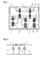
Fig. 1 is a perspective view of a surface acoustic wave (SAW) filter in
accordance with exemplary embodiments of the present invention.
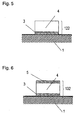
Fig. 2 is a block diagram of the SAW filter in accordance with the
embodiments.
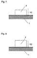
Fig. 3 is a section of a comb electrode, an essential part of a SAW filter
of example 1 in accordance with exemplary embodiment 1 of the present
invention.
Fig. 4 is a section of a comb electrode, an essential part of a SAW filter
of example 2 in accordance with embodiment 1.
Fig. 5 is a section of a comb electrode, an essential part of a SAW filter
of example 3 in accordance with embodiment 1.
Fig. 6 is a section of a comb electrode, an essential part of a SAW filter
of example 4 in accordance with embodiment 1.
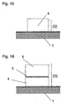
Fig. 7 is a section of a comb electrode, an essential part of a SAW filter
of comparative example 1 in accordance with embodiment 1.
Fig. 8 is a section of a comb electrode, an essential part of a SAW filter
of comparative example 2 in accordance with embodiment 1.
Fig. 9 is a section of a comb electrode, an essential part of a SAW filter
of comparative example 3 in accordance with embodiment 1.
Fig. 10 is a section of a comb electrode, an essential part of a SAW
filter of comparative example 4 in accordance with embodiment 1.
Fig. 11 is a section of a comb electrode, an essential part of a SAW
filter of example 5 in accordance with exemplary embodiment 2 of the
invention.
Fig. 12 is a section of a comb electrode, an essential part of a SAW
filter of example 6 in accordance with embodiment 2.
Fig. 13 is a section of a comb electrode, an essential part of a SAW
filter of example 7 in accordance with embodiment 2.
Fig. 14 is a section of a comb electrode, an essential part of a SAW
filter of example 8 in accordance with embodiment 2.
Fig. 15 is a section of a comb electrode, an essential part of a SAW
filter of comparative example 5 in accordance with embodiment 2.
Fig. 16 is a section of a comb electrode, an essential part of a SAW
filter of example 9 in accordance with exemplary embodiment 3 of the
invention.
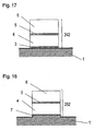
Fig. 17 is a section of a comb electrode, an essential part of a SAW
filter of example 10 in accordance with embodiment 3.
Fig. 18 is a section of a comb electrode, an essential part of a SAW
filter of example 11 in accordance with embodiment 3.
Fig. 19 is a section of a comb electrode, an essential part of a SAW
filter of example 12 in accordance with embodiment 3.
Fig. 20 is a section of a comb electrode, an essential part of a SAW
filter of comparative example 6 in accordance with embodiment 3.
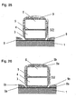
Fig. 21 is a section of a comb electrode, an essential part of each SAW
filter of examples 13 and 14, and comparative examples 7 to 10 in accordance
with exemplary embodiment 4 of the invention.
Fig. 22 is a section of a comb electrode, an essential part of each SAW
filter of examples 15 and 16 in accordance with embodiment 4.
Fig. 23 is a section of a comb electrode, an essential part of each SAW
filter of examples 17 and 18 in accordance with embodiment 4.
Fig. 24 is a section of a comb electrode, an essential part of each SAW
filter of examples 19 and 20 in accordance with exemplary embodiment 5 of
the invention.
Fig. 25 is a section of a comb electrode, an essential part of each SAW
filter of examples 21 and 22 in accordance with embodiment 5.
Fig. 26 is a section of a comb electrode, an essential part of a SAW
filter of example 23 in accordance with embodiment 5.
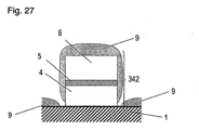
Fig. 27 is a section of a comb electrode, an essential part of a SAW
filter of comparative example 23 in accordance with embodiment 5.
DESCRIPTION OF THE PREFERRED EMBODIMENTS
(Exemplary Embodiment 1)
Fig. 1 is a perspective view of a surface acoustic wave (SAW) filter in
accordance with exemplary embodiments of the present invention, and Fig. 2
is a block diagram of the filter. The SAW filter is a ladder-type surface
acoustic wave filter including substrate 1 and five surface acoustic wave
resonators each including electrode 2 formed on a top surface of substrate 1.
The resonators are coupled in a ladder configuration. Electrode 2 includes
comb electrode 21 and reflector 22. In the embodiments of the invention,
substrate 1 is a 36°-rotated Y-cut lithium tantalate substrate. In exemplary
embodiment 1, a band pass filter including the comb electrode having fingers
disposed by a pitch of 0.6µm and has a center frequency of 1.8GHz.
Figs. 3 to 6 are sections of the electrodes, essential parts of respective
SAW filters of examples 1 to 4 in accordance with embodiment 1. Figs. 7 to
10 are sections of electrodes of respective SAW filters of comparative
examples 1 to 4.
Electrode 102 of example 1, as shown in Fig. 3, includes first layer 4
having a thickness of 200nm formed on substrate 1.
Electrode 112 of example 2, as shown in Fig. 4, includes first layer 4
having a thickness of 200nm and second layer 5 that are stacked over
substrate 1. Second layer 5 prevents the first layer from grain boundary
diffusion of Al atoms occurring in vertical to the substrate.
Electrode 122 of example 3, as shown in Fig. 5, includes base layer 3
and first layer 4 having a thickness of 200nm that are stacked over substrate
1 in this order.
Electrode 132 of Example 4, as shown in Fig. 6, includes base layer 3,
first metal layer 4 having a thickness of 200nm, and layer 5 that are stacked
over substrate 1 in this order. Layer 5 prevents the first metal layer from
grain boundary diffusion.
Electrode 142 of comparative example 1 is, as shown in Fig. 7, metal
layer 4 having a thickness of 200nm formed on substrate 1.
Electrode 152 of comparative example 2 is, as shown in Fig. 8, metal
layer 4 having a thickness of 250nm formed on substrate 1.
Electrode 162 of comparative example 3, as shown in Fig. 9, includes
first metal layer 4 having a thickness of 200nm and second metal layer 5
that are stacked over substrate 1 in this order. Second metal layer 5
prevents the first metal layer from grain boundary diffusion of Al atoms
occurring in vertical to the substrate.
Electrode 172 of comparative example 4, as shown in Fig. 10, includes
first metal layer 3, i.e., a base layer, and second metal layer 4 having a
thickness of 200nm that are stacked over substrate 1 in this order.
Table 1 shows materials for the layers, thicknesses, and methods of
forming the layers of the electrodes of examples 1 to 4 and comparative
examples 1 to 4.
| | Number of Layers | | Base Layer | First Layer | Second Layer | Method of Forming Layers | Section of Electrode |
| Example 1 | 1 | Material | - - | *AlZrCu | -- | IBS | Fig. 3 |
| Thickness | -- | 200 | -- |
| Example 2 | 2 | Material | ― | *AlZrCu | Ti | IBS | Fig. 4 |
| Thickness Thickness | -- | 200 200 | 20 20 |
| Example 3 | 2 | Material | Ti | *AlZrCu | ― | DCMS | Fig. 5 |
| Thickness | 20 | 200 | ― |
| Example 4 | 3 | Material | Ti | *AlZrCu | Ti | DCMS | Fig. 6 |
| Tickness | 10 | 200 | 10 |
| Comparative Example 1 | 1 | Material | | AlZrCu | ― | DCMS | Fig. 7 |
| Thickness | ― | 200 | ― |
| Comparative Example 2 | 1 | Material | ― | *AlZrCu | - | IBS | Fig. 8 |
| Thickness | ― | 250 | ― |
| Comparative Example 3 | 2 | Material | ― | AlZrCu | Ti | DCMS | Fig. 9 |
| Thickness | ― | 200 | 20 |
| Comparative Example 4 | 2 | Material | Cr | AlZrCu | -- | DCMS | Fig. 10 |
| Thickness | 20 | 200 | ― |
| IBS: Ion beam sputtering |
| DCMS: DC magnetron sputtering |
| The asterisk "*" in the "material" column denotes a (111)-oriented layer. |
| All the thicknesses are in nm. |
As shown in Table 1, the metal consisting of Al or consisting mainly of
Al is an AlZrCu alloy in embodiment 1. The electrodes each including the
base layer and/or the second layer employs Ti except for comparative
example 4, which employs Cr for the base layer. The layers are formed by
either ion beam sputtering or DC magnetron sputtering. Having the
electrode layers formed, the electrodes were examined by a -2 X-ray
diffraction method to determine orientation. Regarding the orientation of
examples 1 and 2 and comparative example 2 which use the ion beam
sputtering to form the electrode layers as well as examples 3 and 4 which use
Ti for base layer 3, only a (111) peak of Al for the AlZrCu layers was observed.
It was observed that the Al alloy layer was an oriented layer having a (111)-orientation
in vertical to the substrate. Regarding the other electrode
layers, no peak was observed from a specified crystal plane, and it was
confirmed that they were not oriented layers but non-oriented
polycrystalline layers. In the present embodiment, the Al electrode used for
the filter was designed to have a layer thickness of 200nm. Differences in
characteristics that depend on thicknesses and materials of the electrodes
were adjusted by changing the pitch of the fingers of the comb electrodes,
thus providing the filters with a center frequency of about 1.8GHz. The
electrodes were patterned by photolithography and dry etching and
thereafter diced into chips. Each one of the chips was die-bonded to a
ceramic package and electrically connected by wire bonding. Thereafter, a
cover is welded to it in a nitrogen atmosphere for hermetic sealing it to
provide the SAW filter having the electrodes.
A signal of a highest frequency in a passing band, which is the weakest
point of the ladder type filter, is applied to the filters made in accordance
with the present embodiment for a test for a resistance against an electric
power. The test is suspended periodically for measuring characteristics of
the SAW filter. The filter is verified as degraded at a point where an
insertion loss in the passing band increases by 0.5dB or more, and a total
test time between the starting of the test and the degradation is determined
as a life time. In an accelerated degradation test, an electric power and a
temperature were factors responsible for accelerated degradation. The
accelerated degradation test was conducted on the filter and includes two
kinds of tests. One for determination of the life time under several applied
electric powers with the chip surface maintained in a temperature, and the
other for determination of the life time under several temperatures of the
chip with a constant applied electric power. The Eyring model and the
results of these two tests are used to estimate the life time when the applied
electric power and the environmental temperature are 1W and 50°C,
respectively. A life time of 50,000 hours was qualified as a criteria for
evaluation of the resistance to the electric power. Table 2 shows the
estimated life time of the SAW filters having the electrodes shown in Table 1.
Table 2 also shows crystal grain sizes of the AlZrCu layers of the electrodes.
| | Crystal Grain Size (nm) | Estimated Life Time (hrs) | | Crystal Grain Size (nm) | Estimated Life Time (hrs) |
| Example 1 | 200 | 55,000 | Comparative Example 1 | 200 | 1,500 |
| Example 2 | 200 | 70,000 | Comparative Example 2 | 250 | 12,000 |
| Example 3 | 200 | 56,000 | Comparative Example 3 | 200 | 5 |
| Example 4 | 200 | 74,000 | Comparative Example 4 | 200 | 1,500 |
Table 2 shows that the SAW filters including the electrodes of
examples 1 to 4 have the estimated life time exceeding 50,000 hours, while
the filters of comparative examples 1 to 4 have the estimated life time less
than 50,000 hours. The AlZrCu layer of each of the electrodes has the
crystal grain size substantially identical to a thickness of the layer.
Although the filter of comparative example 2 has the life time less than
50,000 hours, unlike the other comparative examples, the filter has
considerably improved resistance to an electric power. The electrode of
example 1 defers from the electrode of comparative example 2 in a thickness
of the layer and the crystal grain size. A conductive layer has a crystal
grain size increasing in proportion to a thickness of the layer. The SAW
device including a single-layer electrode of the oriented layer as the electrode
layer has a thickness of the electrode of 200nm or less and a life time
exceeding 50,000 hours. With consideration given to variations in
resistance to electric power, the layer preferably has a thickness less than
100nm. According to the above discussion, the layer consisting of Al or
consisting mainly of Al is preferably is an oriented layer having a small
crystal grain size to form an electrode having high resistance to the electric
power. Limiting the layer thickness is effective for reducing the crystal
grain size.
(Exemplary Embodiment 2)
Figs. 11 to 14 are sections of electrodes, essential parts of surface
acoustic wave (SAW) filters of examples 5 to 8 in accordance with exemplary
embodiment 2 of the present invention. Fig. 15 is a section of an electrode
of a SAW filter of comparative example 5.
Electrode 182 of example 5 is, as shown in Fig. 11, first layer 4 having
a thickness of 200nm formed on a top of bump 7 of substrate 1.
Electrode 192 of example 6, as shown in Fig. 12, includes base layer 3
formed on a top of bump 7 of substrate 1 and first layer 4 having a thickness
of 200nm which are stacked in this order over substrate 1.
Electrode 202 of example 7, as shown in Fig. 13, includes first metal
layer 4 having a thickness of 200nm formed on a top of bump 7 of substrate 1
and second layer 5 which are stacked in this order over substrate 1. Second
layer 5 prevents the first metal layer from grain boundary diffusion.
Electrode 212 of example 8, as shown in Fig. 14, includes base layer 3
formed on a top of bump 7 of a substrate, first metal layer 4 having a
thickness of 200nm, and second layer 5 which are stacked in this order over
substrate 1. Second layer 5 prevents the first metal layer from grain
boundary diffusion.
Electrode 222 of comparative example 5 is, as shown in Fig. 15, metal
layer 4 having a thickness of 300nm formed on substrate 1.
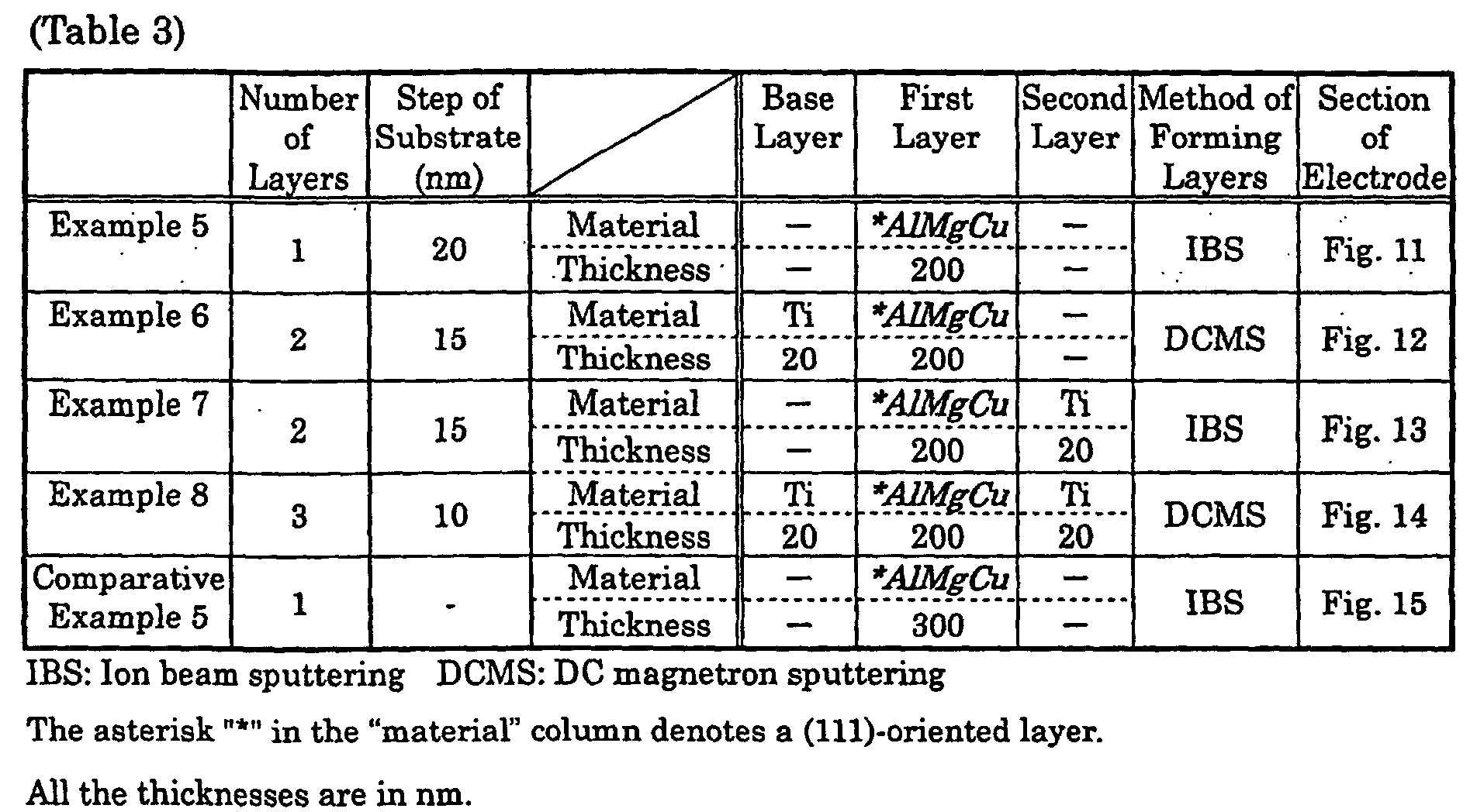
Table 3 shows materials for the layers, thicknesses of the layers, and
methods of forming the layers of the electrodes of examples 5 to 9 and
comparative example 5.
As shown in Table 3, the metal layer consisting of Al or consisting
mainly of Al in embodiment 2 employs an AlMgCu alloy. The electrodes
each having the base layer and/or the second layer use Ti. The layers of the
electrodes are formed by either ion beam sputtering or DC magnetron
sputtering. Having the electrode layers formed, the electrodes were
examined by a -2 X-ray diffraction method to determine orientation.
Regarding the orientation of the AlMgCu layers of examples 5 to 8 and
comparative example 5, only a (111) peak of Al was observed. It was
observed that the Al alloy layer was an oriented layer having a (111)
orientation in vertical to the substrate. The filters of embodiment 2 have
structures identical to those of embodiment 1. The tested filter was
designed to include the Al electrode having a thickness of 300nm and to have
a center frequency of about 1.75GHz. Differences in characteristics that
depend on thicknesses and materials of the electrodes are adjusted by
changing height of the bump of each one of the substrates to provide the
filter with the center frequency of about 1.75GHz.
Thus, the comb electrodes of examples 5 to 8 and comparative example
5 have fingers substantially at the same pitch. The electrodes are
patterned by photolithography and reactive ion etching. Mixed gas
including BC13 and C12 is used as etching gas. Consequently, in the
reactive ion etching, chemical etching with a Cl* radical and a BC13*
radical and sputter etching with a BC13+ ion are carried out simultaneously
for the patterning. The bump of the substrate of each one of examples 5 to 8
is formed by controlling etching time. Subsequently to the patterning, the
substrate is diced into chips. Each one of the chips is die-bonded to a
ceramic package and electrically connected by wire bonding. Thereafter, a
cover is welded in a nitrogen atmosphere for hermetic sealing, thus providing
the SAW filter having the electrode.
The filters made in accordance with
embodiment 2 are evaluated in
the same manner as that of
embodiment 1 in resistance to an electric power.
Table 4 shows an estimated life time of the SAW filters having the electrodes
shown in Table 3. Table 4 also shows crystal grain sizes of AlMgCu layers 4
of the electrodes.
| | Crystal Grain Size (nm) | Estimated Life Time (hrs) | | Crystal Grain Size (nm) | Estimated Life Time (hrs) |
| Example 5 | 200 | 55,000 | Comparative Example 6 | 300 | 9,500 |
| Example 6 | 200 | 56,000 |
| Example 7 | 200 | 70,000 |
| Example 8 | 200 | 74,000 |
As shown in Table 4, each of the SAW filters including the electrodes of
examples 5 to 8 has the estimated life time exceeding 50,000 hours, a criteria,
while the filter of comparative example 5 has the estimated life time less
than 50,000 hours. The AlMgCu layer of each electrode has the crystal
grain size substantially the same as a thickness of the layer. As mentioned
above, the Al electrode of the filter is designed to include the layer having a
thickness of 300nm in embodiment 2. The substrate is provided with the
bump as a part of the electrode, and the metal layer consisting of Al or
consisting mainly of Al has a thickness of 200nm or less. Consequently, the
electrode exhibits the same resistance against an electric power as the
electrodes of examples 1 to 4 described in embodiment 1 and has the life time
of 50,000 hours (the criteria of resistance against an electric power) or more.
As a result, regarding the SAW filter including an electrode including a layer
having a thickness of 200nm or more for exhibiting desired characteristics,
the substrate preferably includes a bump as a part of the electrode, and the
electrode consisting of Al or consisting mainly of Al preferably is an oriented
layer having a thickness of 200nm or less and has a reduced crystal grain
size for having an improved resistance against the electric power.
(Exemplary Embodiment 3)
Figs. 16 to 19 are sections of electrodes which are essential parts of
respective SAW filters of examples 9 to 12 in accordance with exemplary
embodiment 3 of the present invention. Fig. 20 is a section of an electrode
of a SAW filter of comparative example 6.
Electrode 232 of example 9, as shown in Fig. 16, includes first metal
layer 4 having a thickness of 200nm, second layer 5, and third layer 6 which
are stacked in this order over substrate 1. Second layer 5 prevents first
metal layer 4 from grain boundary diffusion of Al atoms occurring in vertical
to the substrate, while third layer 6 is provided for adjusting a thickness of
electrode 232.
Electrode 242 of Example 10, as shown in Fig. 17, includes base layer
3, first metal layer 4 having a thickness of 200nm, second layer 5, and third
layer 6 which are stacked in this order over substrate 1. Second layer 5
prevents first metal layer 4 from grain boundary diffusion of Al atoms
occurring in vertical to the substrate, while third layer 6 is provided for
adjusting a thickness of electrode 242.
Electrode 252 of Example 11, as shown in fig. 18, includes first metal
layer 4 having a thickness of 200nm formed on a top of bump 7 of substrate 1,
second layer 5 for preventing first metal layer 4 from grain boundary
diffusion of Al atoms occurring in vertical to the substrate, and third layer 6
for adjusting a thickness of electrode 252.
Electrode 262 of Example 12, as shown in Fig. 19, includes base layer
3 formed on a top of bump 7 of substrate 1, first metal layer 4 having a
thickness of 200nm, second layer 5, and third layer 6 which are stacked in
this order over substrate 1. Second layer 5 prevents first metal layer 4 from
grain boundary diffusion, while third layer 6 is provided for adjusting a
thickness of electrode 262.
Electrode 272 of comparative example 6, as shown in Fig. 20, includes
base layer 3, first metal layer 4 having a thickness of 200nm, second layer 5,
and third layer 6 which are stacked in this order over substrate 1. Second
layer 5 prevents first metal layer 4 from grain boundary diffusion of Al atoms
occurring in vertical to the substrate, while third layer 6 is provided for
adjusting a thickness of electrode 272.
Table 5 shows materials of the respective layers, thicknesses of the
layers and methods of forming the layers of the electrodes of examples 5 to 9
and comparative example 5.
As shown in Table 5, the metal consisting of Al or consisting mainly of
Al in the present embodiment employs an AlMg alloy, and the base layer and
the second layer employ Ti. The layers are formed by either ion beam
sputtering or DC magnetron sputtering. Having the electrode layers
formed, the electrodes was examined by a -2 X-ray diffraction method to
determine orientation. Regarding the orientation of the AlMg layers of
examples 9 to 12 and comparative example 6, only a (111) peak of Al is
observed, and it is verified that the Al alloy layer is an oriented layer having
a (111) orientation in vertical to the substrate. Since each electrode
includes two AlMg layers, that is, the first layer and the third layer, another
sample including a base layer and a first layer is made under the same
conditions for forming the layers for determining the orientation. The
filters of embodiment 3 have structures identical to those of embodiment 1.
However, the filter including the Al electrode designed to have a thickness of
480nm to have a center frequency of about 800MHz. Differences in
characteristics that depend on thicknesses and materials of the electrodes
are adjusted by changing height of the bump of each substrate and changing
the thickness of the third layer to provide the center frequency of about
800MHz. Thus, the comb electrodes of examples 9 to 12 and comparative
example 6 have fingers at substantially the same pitch. The electrodes and
the filters are made in the same manner as those of embodiment 2.
The filters made in accordance with
embodiment 3 are evaluated in
the same manner as that in
embodiment 1 in respective resistances against
an electric power. Table 6 shows estimated life time of the respective SAW
filters having the respective electrodes shown in Table 5. Table 6 also
shows crystal grain sizes of the respective AlMg layers (the first layers) of
the electrodes.
| | Crystal Grain Size (nm) | Estimated Life Time (hrs) | | Crystal Grain Size (nm) | Estimated Life Time (hrs) |
| Example 9 | 200 | 53,000 | Comparative Example 6 | 280 | 8,800 |
| Example 10 | 200 | 55,000 |
| Example 11 | 200 | 57,000 |
| Example 12 | 200 | 58,000 |
| The crystal grain size represents the crystal grain size of the first layer. |
As shown in Table 6, each SAW filter including the electrode of
examples 9 to 12 has the estimated life time exceeding 50,000 hours, while
the filter of comparative example 6 has the estimated life time less than
50,000 hours. The AlMg layer (the first layer) of each electrode has a
crystal grain size which is substantially the same as a thickness of the layer.
The first metal layer consisting of Al or consisting mainly of Al has a
thickness of 200 nm or less, while the Al electrode of the filter, as described
above, is designed to have a thickness of 480nm in embodiment 2. The
thickness of the first metal layer is set to 200nm or less by providing the
second layer for limiting the thickness of the first layer, and the third layer
for adjusting the thickness of the electrode over the first layer, and/or by
providing the bump as a part of the electrode to the substrate. Accordingly,
the filter has high resistance against an electric power and has the life time
of 50,000 hours (a criteria of evaluation for resistance against an electric
power) or more. After the test, the filters of examples 9 and 10 has a hillock
caused by the diffusion observed at the surface of the comb electrode besides
a degraded portion of the electrode. The diffusion of the Al atoms is caused
by degradation of the third layer adjusting the thickness. The filters of
examples 11 and 12 have no hillock. Thus, the third layer consisting of Al or
consisting mainly ofAl preferably has a thickness of 200nm or less. Further,
a fourth layer may be provided on the third layer to restrain the diffusion of
the Al atoms from the third layer. Although each filter of examples 11 and
12 and comparative example 6 have no hillock caused by the diffusion of the
Al atoms at the surfaces of their respective electrodes after the test, the filter
has a side hillock on opposed faces of the comb electrode. The above results
show that, in order for the SAW filter requiring the thickness of 200nm or
more of the electrode layer for desired characteristics to have the resistance
against an electric power, the second layer and the third layer are preferably
provided over the first layer consisting of Al or consisting mainly of Al and
having the thickness of 200nm or less. The second layer is provided for
limiting the thickness of the first layer, and the third layer is provided for
adjusting the thickness of the electrode layer over the first layer. Moreover,
the crystal grain size can be smaller by the bump as the part of the electrode
provided to the substrate to prevent the third layer from getting thicker, and
by the layer consisting of Al or consisting mainly of Al having thw thickness
of 200nm or less.
(Exemplary Embodiment 4)
Figs. 21 to 23 are sections of electrodes which are essential parts of
respective SAW filters of examples 13 to 8 in accordance with exemplary
embodiment 4 of the present invention. Electrodes of respective SAW filters
of comparative examples 7 to 10 have sections each identical to the electrode
illustrated in Fig. 21.
Each electrode 282 of examples 13 and 14, as shown in Fig. 21,
includes first metal layer 4 having a thickness of 200nm which consists of Al
or consists mainly of Al, second layer 5, and third layer 6 that are stacked in
this order over substrate 1. Second layer 5 prevents the first layer from
grain boundary diffusion of Al atoms occurring in vertical to the substrate,
while third layer 6 adjusts a thickness of electrode 282. Diffusion-preventing
layer 8 is formed on each side of electrode 282 to prevent first
layer 4 from the grain boundary diffusion of the Al atoms and does not reach
the substrate, as shown in Fig. 21.
Each electrode 292 of examples 15 and 16, as shown in Fig. 22,
includes base layer 3, first metal layer 4 having 200nm, second layer 5, and
third layer 6 that are stacked in this order over substrate 1. Second layer 5
prevents first metal layer 4 from grain boundary diffusion of Al atoms
occurring in vertical to the substrate, while third layer 6 adjusts a thickness
of electrode 292. Diffusion-preventing layer 8 is formed on each side of
electrode 292 to prevent first metal layer 4 from the grain boundary diffusion
of the Al atoms. The diffusion-preventing layer 8 does not reach the
substrate, but covers the sides of first metal layer 4, second layer 5, third
layer 6, and a part of each side of base layer 3, as shown in Fig. 22.
Each electrode 302 of examples 17 and 18, as shown in Fig. 23,
includes first metal layer 4 having a thickness of 200nm formed on a top of
bump 7 of substrate 1, second layer 5 for preventing first metal layer 4 from
grain boundary diffusion of Al atoms occurring in vertical to the substrate,
and third layer 6 for adjusting a thickness of electrode 302. Diffusion-preventing
layer 8 is formed on each side of electrode 302 to prevent first
metal layer 4 from the grain boundary diffusion of the Al atoms. As shown
in Fig. 23, diffusion-preventing layer 8 does not reach a bottom of the
substrate, but covers each side of first metal layer 4, second layer 5, third
layer 6, and a part of each side of bump 7 of substrate 1.
Electrodes of comparative examples 7 to 10 have structures identical
to those of examples 13 and 14 illustrated by Fig. 21.
Table 7 shows materials of the layers, thicknesses of the layers, and
methods of forming the layers of the electrodes of examples 13 to 18 and
comparative examples 7 to 10.
As shown in Table 7, an AlMg alloy is used as metal of layer 4
consisting of Al or consisting mainly of Al in the fourth embodiment, and Ti
is used for the base layer. Ti is used for the second layers of examples 13, 15,
and 17, and comparative examples 7 and 8, while Cu is used for the second
layers of examples 14, 16, and 18 and comparative examples 8 and 10. The
layers are formed by either ion beam sputtering or DC magnetron sputtering.
Having the electrode layers formed, the electrodes were examined by a -2
X-ray diffraction method to determine orientation of the electrodes.
Ragarding the orientation of the AlMg layers of examples 13 to 18 and
comparative examples 9 and 10, only a (111) peak of Al was observed, and
thus the Al alloy layers are verified to be layers having a (111)-orientation in
vertical to the substrate. Since each electrode includes two AlMg layers,
that is, the first layer and the third layer, another sample having two layers,
that is, a base layer and a first layer was prepared under the same conditions
of the layer formation for the determination of the orientation. For
comparative examples 7 and 8, no peak was observed from a specified crystal
plane, and thus the layers of the samples are not verified to be oriented
layers, but non-oriented polycrystalline layers. The filters of embodiment 4
have structure and design to those of embodiment 3. The electrodes are
patterned by Ar+ ion milling. In the ion milling, since the patterning is
physically carried out through sputtering, some sputtered atoms adhere to a
side of the electrode, thus enabling the diffusion-preventing layer to be
formed simultaneously to the patterning. However, the diffusion-preventing
layer does not cover the entire side of the electrode, thus not
reaching a bottom of the substrate.
Table 8 shows an estimated live time of a SAW filter having each
electrode shown in Table 7. Table 8 also shows crystal grain sizes of the
respective AlMg layers, the first layers of the electrodes.
| | Crystal Grain Size (nm) | Estimated Life Time (hrs) | | Crystal Grain Size (nm) | Estimated Life time (hrs) |
| Example 13 | 200 | 58,000 | Comparative Example 7 | 200 | 14 |
| Example 14 | 200 | 63,000 | Comparative Example 8 | 200 | 170 |
| Example 15 | 200 | 85,000 | Comparative Example 9 | 300 | 120 |
| Example 16 | 200 | 100,000 | Comparative Example 10 | 300 | 1200 |
| Example 17 | 200 | 85,000 |
| Example 18 | 200 | 100,000 |
| The crystal grain size represents the crystal grain size of the first layer. |
As shown in Table 8, the SAW filter each including the electrodes of
examples 13 to 18 have the estimated life time exceeding 50,000 hours (the
criteria), while the filter of comparative examples 7 to 10 has the estimated
life time less than 50,000 hours. The AlMg layer, the first layer of each
electrode has the crystal grain size substantially the same as a thickness of
the layer. After the test, in examples 13 and 14 and comparative examples,
a side hillock was at a side of the comb electrode besides a degraded portion
of the electrode. The side hillock is formed between the substrate and the
diffusion-preventing layer on each side of the electrode to prevent the first
metal layer from the grain boundary diffusion of the Al atoms. Examples 15
to 18 had no degradation of the electrode except for a degraded portion of the
electrode. This shows that the grain boundary diffusion of the Al atoms
through each side of the electrode is restrained with the diffusion preventing
layer covering the part of the base layer or the part of each side of the bump
of the substrate and covering the entire first metal layer.
The filters each including the second layer of Ti has larger resistance
against an electric power than the filters each including the second layer of
Cu. Since Cu has a diffusion coefficient to Al larger than a self-diffusion
coefficient of Al, Cu atoms diffuse along grain boundaries in the second layer
at a heating process in a manufacturing process for the filter, thereby
obstructing a path of the grain boundary diffusion of Al atoms. For this
reason, the grain boundary diffusion of the Al atoms in horizontal direction
to the substrate is restrained. Cu easily diffuses easily into Al, and further,
easily forms metallic compound with Al, and has the grain size grow in the
second layer. Therefore, a change in temperature during the process and a
thickness of the Cu layer influence an effect of restraining the Al atoms. A
resistance of the electrode layer easily increases. Thus the filters have
characteristics and resistance against an electric power and characteristics
ranging widely.
The second layer containing the metal having the larger diffusion
coefficient to Al than the self-diffusion coefficient of Al having large
resistance against an electric power. The layer has an optimum thickness,
thus requiring the manufacturing process, particularly the heating process
to be controlled. If the thickness of the first metal layer consisting of Al or
consisting mainly of Al is 200nm or less, the thickness of the second layer of
Cu is preferably 20nm or less, more preferably 10nm or less. Moreover, the
heating process is carried out preferably at 250°C or less, more preferably at
200°C or less.
The second layer containing metal having a diffusion coefficient to Al
smaller than the self-diffusion coefficient of Al is expected to be less effective
for restraining the grain boundary diffusion of the Al atoms in the first metal
layer consisting of Al or consisting mainly of Al that occurs in horizontal to
the substrate, but enables the filter to have stabile resistance against an
electric power and stable characteristics.
These facts show that the diffusion-preventing layer covering each
entire side of the first layer effectively restrains the grain boundary diffusion
of the Al atoms of the first metal layer consisting ofAl or consisting mainly of
Al that occurs in horizontal to the substrate. The diffusion-preventing
layer may be formed by the patterning carried out through sputtering
etching. The base layer or the bump formed by grinding the substrate is
effective. The diffusion-preventing layer formed on each side of the
electrode by the method naturally become a laminated layer or an alloy layer
with the first metal layer consisting of Al or consisting mainly of Al and
either the base layer or the material of the substrate, thus having large
resistance against migration
(Exemplary Embodiment 5)
Figs. 24 to 26 are sections of electrodes which are essential parts of
respective SAW filters of examples 19 to 23 in accordance with exemplary
embodiment 5. Fig. 27 is a section of an electrode of a SAW filter of
comparative Example 11.
Each electrode 312 of examples 19 and 20, as shown in Fig. 24,
includes first metal layer 4 of a 200nm thickness on a top of bump 7 of
substrate 1, second layer 5 for preventing the first metal layer from grain
boundary diffusion of Al atoms occurring in vertical to the substrate, and
third layer 6 for adjusting a thickness of electrode 312. After the electrode
is patterned, protective layer 9 is formed over electrode 312. Protective
layer 9 of example 19 is made of silicon nitride and has a thickness of 100nm,
while protective layer 9 of example 20 is made of silicon oxide and has a
thickness of 100nm. According to an observation with an electron
microscope, the protective layer was not formed about the bump of the
substrate, specifically about a boundary between the comb electrode and a
bottom of the substrate between the electrodes, thus being discontinuously
formed, as shown in Fig. 24.
Each electrode 322 of examples 21 and 22, as shown in Fig. 25,
includes base layer 3, first metal layer 4 having a 200nm-thickness, second
layer 5, and third layer 6 that are stacked in this order over substrate 1.
Second layer 5 prevents the first layer from grain boundary diffusion of Al
atoms occurring in vertical to the substrate, while third layer 6 adjusts a
thickness of electrode 322. After electrode 322 is formed, protective layer 9
is formed over electrode 322. Protective layer 9 of example 21 is made of
i silicon nitride and has a thickness of 100nm, while protective layer 9 of
example 22 is made of silicon oxide and has a thickness of 100nm.
According to an observation with an electron microscope, protective layer 9
was not formed about a boundary between base layer 3 and a bottom of
substrate 1, as shown in Fig. 25.
Electrode 332 of example 23, as shown in Fig. 26, includes base layer 3,
first metal layer 4 of a 200nm-thickness, second layer 5, and third layer 6
that are stacked in this order over substrate 1. Second layer 5 prevents the
first metal layer from grain boundary diffusion of Al atoms occurring in
vertical to the substrate, while third layer 6 adjusts a thickness of electrode
332. After electrode 332 is formed, silicon nitride layer 9a of a 50nm-thickness
and silicon oxide layer 9b of 50nm-thickness are formed over
electrode 332. According to an observation with an electron microscope,
protective layers 9a and 9b are not formed about a boundary between base
layer 3 and a bottom of substrate 1, as shown in Fig. 26.
Electrode 342 of comparative example 11, as shown in Fig. 27,
includes first metal layer 4 of a 200nm-thickness, second layer 5 for
preventing the first metal layer from grain boundary diffusion of Al atoms
occurring in vertical to the substrate, and third layer 6 for adjusting a
thickness of electrode 342. After the electrode is formed, protective layer 9
of a 100nm-thickness made of silicon nitride is formed over electrode 342.
According to an observation with an electron microscope, protective layer 9
was not formed about a boundary between electrode 342 and a bottom of
substrate 1, as shown in Fig. 27.
Table 9 shows materials of the layers, thicknesses of the layers, and
methods of forming the layers of the electrodes of examples 19 to 23 and
comparative example 11.
As shown in Table 9, an AlMg alloy is used as the metal consisting of
Al or consisting mainly of Al in
embodiment 5, and Ti is used for
base layers
3 and
second layers 5. The layers are formed by either ion beam sputtering
or DC magnetron sputtering. Having the electrode layers formed the
electrodes were examined by a -2 X-ray diffraction method to determine
orientation. Regarding the orientation of the AlMg layers of examples 19 to
23 and comparative example 11, only a (111) peak of Al was observed. Thus,
it is verified that the Al alloy layer is a (111)-orientation in vertical to the
substrate. Since each sample includes two AlMg layers, that are the first
layer and the third layer, another sample having a first layer and a still
another sample having a base layer and a first layer are made under the
same conditions of the layer formation for determination of their orientation.
The filters of the present embodiment have structures identical to those of
the first embodiment. The filter is provided with the Al electrode having a
thickness of 480nm to have a center frequency of about 800MHz. The
electrodes are formed by photolithography and dry etching. After the
electrodes are formed, a protective layer is formed. And a portion of the
protective layer for electrical connection is then removed by etching, and a
resulting resonator is mounted on an alumina substrate to face down toward
the substrate. In the present embodiment, the filters are not hermetically
sealed. The filters of this embodiment are evaluated in the same manner as
in the first embodiment in respective resistances against electric power.
The filters, which include the protective layers, are evaluated while having
their respective surfaces exposed to atmospheric air. Table 10 shows an
estimated life time of each SAW filter having the electrodes shown in Table 9.
Table 10 also shows crystal grain sizes of the AlMg layers (the first layers) of
the electrodes.
| | Crystal Grain Size (nm) | Estimated Life Time (hrs) | | Crystal Grain Size (nm) | Estimated Life Time (hrs) |
| Example 19 | 200 | 60,000 | Comparative Example 11 | 200 | 320 |
| Example 20 | 200 | 65,000 |
| Example 21 | 200 | 60,000 |
| Example 22 | 200 | 65,000 |
| Example 23 | 200 | 65,000 |
| The crystal grain size represents the crystal grain size of the first layer. |
As shown in Table 10, the SAW filters including the respective
electrodes of examples 13 to 18 have the estimated life time exceeding 50,000
hours (a criteria), while the filter of comparative examples 7 to 10 has the
estimated life of less than 50,000 hours. The AlMg layer (the first layer) of
each electrode has the crystal grain size substantially the same as a
thickness of the electrode. It is apparent that the filters of examples 19 and
21 each provided with the protective layer of silicon nitride have improved
resistance against electric power as compared with the filters of examples 20
and 22 each provided with the protective layer of silicon oxide. It was
observed that the filters have electric characteristics slightly degraded after
they have the protective layer of silicon nitride formed, while the filters have
no changes in electric characteristics even after they have the protective
layer of silicon oxide formed. The filter of example 23 including the
laminated protective layer of silicon nitride and silicon oxide exhibited no
change in electric characteristics even after the filter had the protective
layers formed. It was observed that the filter had an improved resistance
against electric power that was similar to that of the filter including only the
silicon nitride. Although the filter of comparative example 11 has an
electrode structure identical to that of example 13 of embodiment 4 and to
have an excellent resistance against electric power, the filter has a short
estimated life of 320 hours. Conceivably, this is because the filters are not
hermetically sealed in embodiment 5. The filters of examples 19 to 23
exhibit substantially the same level of resistance against electric power as
the filters hermetically sealed. It is conceivable from this fact that the filter
of comparative example 11 has the short life time since its first metal layer
consisting of Al or consisting mainly of Al is partially exposed, not being
entirely covered by the protective layer. The protective layer easily has a
discontinuous portion as shown in each of Figs. 25 to 27 about a boundary
between the electrode and a bottom of the substrate where the protective
layer on the electrodes is thin. If such a discontinuous portion is formed, it
is apparent that the bump to the substrate or the base metal layer having
excellent moisture resistance in the present embodiment is effective for
extending the life time of the filter.
The protective layer prevents the electrode from a hillock caused by
migration of the Al atoms, thus improving the resistance against electric
power, preventing the electrodes from a short circuit between them, and
improving moisture resistance.
In embodiment 5, the electrode is constructed to have the resistance
against electric power and the moisture resistance due to the protective layer.
The protective layer on the electrode provided with the bump at the
substrate or the base layer having the excellent moisture resistance is
effective for extending the life time of the filter.
In embodiments 1 to 5, the structures of the electrodes for specified
filters are described. However, the present invention is not limited to the
structures, the thicknesses, the materials and others of the layers described
in the embodiments. In particular, the thickness of the layer consisting of
Al or consisting mainly of Al is preferably 0.01·L or less, where L is a width
of the electrode of the SAW filter. Thus, conductive powder can be
sufficiently fine, whereby stress on the electrode that is caused by
propagation of surface acoustic waves can be sufficiently dispersed.
INDUSTRIAL APPLICABILITY
The present invention provides a surface acoustic wave filter having
improved resistance against stress caused by propagation of surface acoustic
waves, and a method of manufacturing the filter.