EP1329991A1 - Press contact clamping connector and its connection structure - Google Patents
Press contact clamping connector and its connection structure Download PDFInfo
- Publication number
- EP1329991A1 EP1329991A1 EP01974667A EP01974667A EP1329991A1 EP 1329991 A1 EP1329991 A1 EP 1329991A1 EP 01974667 A EP01974667 A EP 01974667A EP 01974667 A EP01974667 A EP 01974667A EP 1329991 A1 EP1329991 A1 EP 1329991A1
- Authority
- EP
- European Patent Office
- Prior art keywords
- pin
- conductive
- compression type
- toe
- type connector
- Prior art date
- Legal status (The legal status is an assumption and is not a legal conclusion. Google has not performed a legal analysis and makes no representation as to the accuracy of the status listed.)
- Granted
Links
- 230000006835 compression Effects 0.000 claims abstract description 94
- 238000007906 compression Methods 0.000 claims abstract description 94
- 229910000679 solder Inorganic materials 0.000 description 14
- 230000001413 cellular effect Effects 0.000 description 9
- 230000008602 contraction Effects 0.000 description 8
- 230000000694 effects Effects 0.000 description 8
- 230000002265 prevention Effects 0.000 description 8
- -1 specifically Substances 0.000 description 8
- 229920000122 acrylonitrile butadiene styrene Polymers 0.000 description 7
- 238000000034 method Methods 0.000 description 7
- 239000000523 sample Substances 0.000 description 6
- 229910001369 Brass Inorganic materials 0.000 description 5
- RYGMFSIKBFXOCR-UHFFFAOYSA-N Copper Chemical compound [Cu] RYGMFSIKBFXOCR-UHFFFAOYSA-N 0.000 description 5
- 239000010951 brass Substances 0.000 description 5
- 229910052802 copper Inorganic materials 0.000 description 5
- 239000010949 copper Substances 0.000 description 5
- 235000012489 doughnuts Nutrition 0.000 description 5
- 229920001971 elastomer Polymers 0.000 description 5
- 239000000806 elastomer Substances 0.000 description 5
- 239000004973 liquid crystal related substance Substances 0.000 description 5
- 239000011159 matrix material Substances 0.000 description 5
- 238000005476 soldering Methods 0.000 description 5
- 229910052782 aluminium Inorganic materials 0.000 description 4
- XAGFODPZIPBFFR-UHFFFAOYSA-N aluminium Chemical compound [Al] XAGFODPZIPBFFR-UHFFFAOYSA-N 0.000 description 4
- 238000006073 displacement reaction Methods 0.000 description 4
- PCHJSUWPFVWCPO-UHFFFAOYSA-N gold Chemical compound [Au] PCHJSUWPFVWCPO-UHFFFAOYSA-N 0.000 description 4
- 239000010931 gold Substances 0.000 description 4
- 229910052737 gold Inorganic materials 0.000 description 4
- 239000000463 material Substances 0.000 description 4
- 230000002093 peripheral effect Effects 0.000 description 4
- 239000004698 Polyethylene Substances 0.000 description 3
- 239000004743 Polypropylene Substances 0.000 description 3
- 238000007747 plating Methods 0.000 description 3
- 229920000515 polycarbonate Polymers 0.000 description 3
- 239000004417 polycarbonate Substances 0.000 description 3
- 229920000573 polyethylene Polymers 0.000 description 3
- 229920001155 polypropylene Polymers 0.000 description 3
- 238000009751 slip forming Methods 0.000 description 3
- 229910000906 Bronze Inorganic materials 0.000 description 2
- PXHVJJICTQNCMI-UHFFFAOYSA-N Nickel Chemical compound [Ni] PXHVJJICTQNCMI-UHFFFAOYSA-N 0.000 description 2
- 230000002411 adverse Effects 0.000 description 2
- 239000010974 bronze Substances 0.000 description 2
- 239000004020 conductor Substances 0.000 description 2
- KUNSUQLRTQLHQQ-UHFFFAOYSA-N copper tin Chemical compound [Cu].[Sn] KUNSUQLRTQLHQQ-UHFFFAOYSA-N 0.000 description 2
- 239000006071 cream Substances 0.000 description 2
- 229920006351 engineering plastic Polymers 0.000 description 2
- 229920002379 silicone rubber Polymers 0.000 description 2
- 239000004945 silicone rubber Substances 0.000 description 2
- 244000043261 Hevea brasiliensis Species 0.000 description 1
- OAICVXFJPJFONN-UHFFFAOYSA-N Phosphorus Chemical compound [P] OAICVXFJPJFONN-UHFFFAOYSA-N 0.000 description 1
- 239000005062 Polybutadiene Substances 0.000 description 1
- 230000001154 acute effect Effects 0.000 description 1
- 229910052790 beryllium Inorganic materials 0.000 description 1
- ATBAMAFKBVZNFJ-UHFFFAOYSA-N beryllium atom Chemical compound [Be] ATBAMAFKBVZNFJ-UHFFFAOYSA-N 0.000 description 1
- 238000007796 conventional method Methods 0.000 description 1
- 230000014759 maintenance of location Effects 0.000 description 1
- 229910052751 metal Inorganic materials 0.000 description 1
- 239000002184 metal Substances 0.000 description 1
- 229920003052 natural elastomer Polymers 0.000 description 1
- 229920001194 natural rubber Polymers 0.000 description 1
- 229910052759 nickel Inorganic materials 0.000 description 1
- 229920003023 plastic Polymers 0.000 description 1
- 239000004033 plastic Substances 0.000 description 1
- 239000000088 plastic resin Substances 0.000 description 1
- 229920001084 poly(chloroprene) Polymers 0.000 description 1
- 229920002857 polybutadiene Polymers 0.000 description 1
- 229920001195 polyisoprene Polymers 0.000 description 1
- 229920003225 polyurethane elastomer Polymers 0.000 description 1
- 229910001220 stainless steel Inorganic materials 0.000 description 1
- 239000010935 stainless steel Substances 0.000 description 1
- 238000004804 winding Methods 0.000 description 1
Images








Classifications
-
- H—ELECTRICITY
- H01—ELECTRIC ELEMENTS
- H01R—ELECTRICALLY-CONDUCTIVE CONNECTIONS; STRUCTURAL ASSOCIATIONS OF A PLURALITY OF MUTUALLY-INSULATED ELECTRICAL CONNECTING ELEMENTS; COUPLING DEVICES; CURRENT COLLECTORS
- H01R13/00—Details of coupling devices of the kinds covered by groups H01R12/70 or H01R24/00 - H01R33/00
- H01R13/02—Contact members
- H01R13/10—Sockets for co-operation with pins or blades
- H01R13/14—Resiliently-mounted rigid sockets
-
- H—ELECTRICITY
- H01—ELECTRIC ELEMENTS
- H01R—ELECTRICALLY-CONDUCTIVE CONNECTIONS; STRUCTURAL ASSOCIATIONS OF A PLURALITY OF MUTUALLY-INSULATED ELECTRICAL CONNECTING ELEMENTS; COUPLING DEVICES; CURRENT COLLECTORS
- H01R13/00—Details of coupling devices of the kinds covered by groups H01R12/70 or H01R24/00 - H01R33/00
- H01R13/02—Contact members
- H01R13/22—Contacts for co-operating by abutting
- H01R13/24—Contacts for co-operating by abutting resilient; resiliently-mounted
- H01R13/2407—Contacts for co-operating by abutting resilient; resiliently-mounted characterized by the resilient means
- H01R13/2421—Contacts for co-operating by abutting resilient; resiliently-mounted characterized by the resilient means using coil springs
-
- H—ELECTRICITY
- H01—ELECTRIC ELEMENTS
- H01R—ELECTRICALLY-CONDUCTIVE CONNECTIONS; STRUCTURAL ASSOCIATIONS OF A PLURALITY OF MUTUALLY-INSULATED ELECTRICAL CONNECTING ELEMENTS; COUPLING DEVICES; CURRENT COLLECTORS
- H01R12/00—Structural associations of a plurality of mutually-insulated electrical connecting elements, specially adapted for printed circuits, e.g. printed circuit boards [PCB], flat or ribbon cables, or like generally planar structures, e.g. terminal strips, terminal blocks; Coupling devices specially adapted for printed circuits, flat or ribbon cables, or like generally planar structures; Terminals specially adapted for contact with, or insertion into, printed circuits, flat or ribbon cables, or like generally planar structures
- H01R12/70—Coupling devices
- H01R12/7076—Coupling devices for connection between PCB and component, e.g. display
-
- H—ELECTRICITY
- H01—ELECTRIC ELEMENTS
- H01R—ELECTRICALLY-CONDUCTIVE CONNECTIONS; STRUCTURAL ASSOCIATIONS OF A PLURALITY OF MUTUALLY-INSULATED ELECTRICAL CONNECTING ELEMENTS; COUPLING DEVICES; CURRENT COLLECTORS
- H01R12/00—Structural associations of a plurality of mutually-insulated electrical connecting elements, specially adapted for printed circuits, e.g. printed circuit boards [PCB], flat or ribbon cables, or like generally planar structures, e.g. terminal strips, terminal blocks; Coupling devices specially adapted for printed circuits, flat or ribbon cables, or like generally planar structures; Terminals specially adapted for contact with, or insertion into, printed circuits, flat or ribbon cables, or like generally planar structures
- H01R12/70—Coupling devices
- H01R12/71—Coupling devices for rigid printing circuits or like structures
- H01R12/712—Coupling devices for rigid printing circuits or like structures co-operating with the surface of the printed circuit or with a coupling device exclusively provided on the surface of the printed circuit
- H01R12/714—Coupling devices for rigid printing circuits or like structures co-operating with the surface of the printed circuit or with a coupling device exclusively provided on the surface of the printed circuit with contacts abutting directly the printed circuit; Button contacts therefore provided on the printed circuit
Definitions
- the present invention relates to a compression type connector and its connecting structure for use in electrical connection between an electronic circuit board and liquid crystal module, connection between multiple electronic circuit boards, connection between a certain type of IC package and an electronic circuit board and connection of an electronic circuit board with a microphone, speaker or the like of a cellular phone or a portable information terminal.
- any of the following techniques can be used: (1) a method of using a compression type connector with a multiple number of metallic fine wires arranged in a row on the curved surface of an elastomer piece having an approximately semielliptical section or approximately U-shaped section; (2) a method of using the connector pins for electrical connection disclosed in Japanese Patent Application Laid-open Hei 7-161401; and (3) a method of creating connection by soldering conductive wires between the electrodes of an electronic circuit board and an electroacoustic part.
- the present invention has been devised in view of the above circumstances, it is therefore an object of the present invention to provide a compression type connector which is low in height and hence can reduce the route of conduction and enables low-load connections. It is another object to provide a connecting structure of a compression type connector which can be improved in positioning accuracy and assembly performance. It is a further object to provide a connecting structure of a compression type connector which can make the work simple by omitting soldering.
- the invention defined in Claim 1 comprises: a conductive toe-pin having a cap-like shape; a conductive pin fitted into the conductive toe-pin in a slidable manner; and a spring fitted on conductive pin, and is characterized in that the spring rests on the opening end face of the conductive toe-pin so as to urge the conductive pin in the direction opposite the bottom of the conductive-toe pin.
- the invention defined in Claim 2 is characterized in that an insulative housing to be interposed between opposing electrodes has a multiple number of passage holes formed therein, and a compression type connector defined in Claim 1 is fitted in each passage hole in such a manner that the bottom of the conductive toe-pin of the compression type connector is projected from one side of the housing and the conductive pin of the compression type connector is projected on the other side of the housing.
- the invention defined in Claim 3 is characterized in that an insulative holder to be interposed between opposing electrodes is formed in an approximate cylinder with a bottom and has a multiple number of passage holes formed in the bottom, and a compression type connector defined in Claim 1 is fitted in each passage hole in such a manner that the bottom of the conductive toe-pin of the compression type connector is projected from one side of the holder's bottom and the conductive pin of the compression type connector is projected on the other side of the holder's bottom, toward the open side.
- the end faces of the conductive toe-pin and conductive pin defined in the Claims may be formed, as appropriate, in a pointed form of a predetermined angle, a form having a semicircular section, semi-elliptic section or semi-oval section, a form having a single or multiple pins, a crown shape, a tooth-like pin-joint dowel form (dowel: architecture technical term), dowel rivet form (dowel: architecture technical term) and the like.
- the end part of the conductive toe-pin or conductive pin is formed with a pointed form such as a conical or pyramidal form, the oxide film over the solder of the electrode can be broken so as to establish a good conduction.
- the housing may be rectangular, square, polygonal, elliptic or oval or of other shapes.
- Examples of the electrically joined object having electrodes include assorted types of circuit boards, test circuit boards, liquid crystal modules (COG, COF, TAB and the like), assorted types of IC packages such as surface mount types (QFP, BGA, LGA, etc.), various electronic parts such as microphones, speakers and others of a cellular phone or electronic device.
- a multiple number of the compression type connectors defined in Claim 1 are embedded in an insulative housing or holder, either directly or indirectly, but this should not be limit the invention: a single connector may be arranged alone.
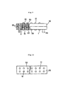
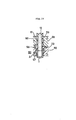
- a miniature compression type connector in the present embodiment includes: as shown in Figs.1 through 3, a cap-like conductive toe-pin 1, a conductive pin 10 fitted and slidably supported within conductive toe-pin 1 and a coil spring 20 fitted on conductive pin 10 and repulsively urging the conductive pin 10 upwards or in the opposite direction to the bottom of conductive toe-pin 1.
- a multiple number of the compression type connectors are arranged in an insulative housing 50 interposed between electrodes 31 and 41 of an electronic circuit board 30 and an electrically joined object 40, each opposing the other, so as to provide electrical conduction between electronic circuit board 30 and electrically joined object 40.
- conductive toe-pin 1 is formed of, for example, a cylinder with a bottom having an approximately U-shaped section, with gold-plated conductive material, specifically, copper, brass or aluminum.
- the conductive toe-pin 1 may be put into contact, at its flat bottom which is marginally projected from the undersurface (bottom side) as one side of housing 50, with electrode 31 of electronic circuit board 30, or may be appropriately fixed to electrode 31 of electronic circuit board 30 with a solder layer, ACF (anisotropic conductive film) or the like, so as to secure conduction.
- the projected amount of the bottom of conductive toe-pin 1 is about 0.1 to 1.5 mm, preferably 0.1 to 1.0 mm.
- conductive pin 10 may be, for example, formed of conductive elastomer or conductive copper, brass or aluminum plated with gold and shaped in a cylindrical form. This conductive pin 10 is formed so that an upper part is made smaller in diameter and the head is formed of a large diametric conical or semispherical form, so that the end face of the head comes into acute or smooth contact with electrode 41 of electrically joined object 40.
- Coil spring 20 is formed in an approximately frustoconical shape, by winding a predetermined metallic fine wire having a diameter of, for example, 30 to 100 ⁇ m or preferably 30 to 80 ⁇ m, with a pitch of 50 ⁇ m, for example, and placed on the upper end face of the opening of conductive toe-pin 1, so as to produce a load of 30g to 60g when compressed by 0.5 mm.
- metallic fine wire for forming this coil spring 20
- the reason for the diameter of the metallic fine wire being limited within the range of 30 to 80 ⁇ m is that selection of a value from this range makes it easy to realize a low-cost and low-load connection.
- the length of coil spring 20 should be, for example, 0.5 to 3.0 mm, preferably 1.0 to 1.5 mm. It is preferred that about half of its length is exposed above and beyond the upper face (obverse face) as the other side of housing 50. Limiting the length within the above range makes it possible to shut out adverse effect due to noise from the outside and maintain the resilient characteristics.
- the top part of coil spring 20 is formed smaller in diameter than the bottom part, lower part, middle part and upper part, as shown in the same drawing, and is fitted to the groove of the upper part of conductive pin 10 so as to prevent the pin from dislodging and coming off, in a markedly effective manner.
- the diameter at the top part of coil spring 20 is formed smaller by 0.05 to 0.2 mm than that of the middle portion. This limitation is given because there is a possibility that conductive pin 10 will not smoothly fit into conductive toe-pin 1 if the upper part of coil spring 20 has the same diameter as the upper part of conductive pin 10.
- electronic circuit board 30 may be a printed circuit board, for example, of which multiple electrodes 31 are laid out flat on its surface, and a solder layer consisting of cream solder, ACF or the like is formed on each electrode 31 when the board is connected for conduction.
- electrically joined object 40 may be a COG liquid crystal module, for example, and is arranged closely opposing the surface of electronic circuit board 30, located below.
- This electrically joined object 40 has multiple electrodes 41 constituted of ITO.
- housing 50 is formed of a thin, flat rectangular, or plate-like, monolayered piece using a predetermined material, with multiple small-diametric passage holes 51 bored in the direction of its thickness and arranged lengthwise in a row at intervals of a predetermined pitch.
- This elongated housing 50 can be formed of multi-purpose engineering plastic which is excellent in heat resistance, dimensional stability, moldability and the like (for example, ABS resin, polycarbonate, polypropylene, polyethylene, etc.). Among these, ABS resin is the most suitable in view of workability and cost.
- the multiple passage holes 51 are formed with a pitch of about 0.5 to 1.27 mm, for example.
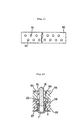
- Each passage hole 51 is comprised of, as shown in Figs. 2 and 3, a large-height fitting bore 52 located on the electronic circuit board 30 side into which conductive toe-pin 1 snugly fits, a sectioned bore 53 which is formed continuously from the upper part of fitting bore 52, creating a space above the top rim of the opening of conductive toe-pin 1, and a reduced-diameter bore 54 located on the electrically joined object 40 side, above a step formed at the top end of sectioned bore 53, all being continuously formed.
- Conductive toe-pin 1 is fitted from the underside of fitting bore 52 and fixed therein, with its bottom part marginally exposed downward from the undersurface of housing 50.
- the united conductive pin 10 and coil spring 20 are fitted into sectioned bore 53 so that the bottom end of coil spring 20 is tightly fitted. This tight fitting provides effective prevention of coil spring 20 falling off.
- the compression type connector is positioned and fixed to electronic circuit board 30. Then the compression type connector is positioned and held between electronic circuit board 30 and electrically joined object 40 so that each electrode 31 of electronic circuit board 30 comes into surface contact with conductive toe-pin 1 while each electrode 41 of electrically joined object 40 comes into contact with repulsive conductive pin 10.
- each coil spring 20 contracts and conductive pin 10 with its top part projected above housing 50 moves down into conductive toe-pin 1, whereby electrical connection between electronic circuit board 30 and electrically joined object 40 can be repulsively achieved via conductive toe-pin 1 and conductive pin 10 (see Fig.1).
- the height of the compression type connector can be made short (about 1.50 mm to 2.00 mm) without any difficulty and it is also possible to realize a low-resistance and low-load connection (e.g., 30g to 60g/pin).
- conductive toe-pin 1 which is excellent in stability and mountability is fitted and plugged into each passage hole 51 while conductive pin 10 is put into contact with electrode 41 of electrically joined object 40, establishment of stable conduction can be highly expected.
- conductive toe-pin 1 and conductive pin 10 are put into regular contact with each other by their peripheries to create the shortest route of conduction, it is possible to shorten the route of conduction and hence markedly reduce the inductance and achieve improved high-frequency characteristics, in contrast to the case where conduction path is formed only by a long coil spring which is spirally wound. It is also possible to shorten the length of conductive pin 10. Further, since the compression type connector is held between electronic circuit board 30 and electrically joined object 40, by means of housing 50, it is possible to easily assemble or mount the compression type connector into electronic circuit board 30, hence markedly improve the positioning accuracy and assembly performance.
- conductive pin 10 When the head of conductive pin 10 is formed so as to be semispherical or semi-spheroidal, stable conduction can be secured even if, for example, coil spring 20 becomes tilted left and right or back and forth. Further, since the bottom part of coil spring 20 is held by sectioned bore 53 and conducive toe-pin 1, it is possible to prevent coil spring 20 from dislodging by a simple arrangement. Still more, since coil spring 20 is formed of a locally stepped and tapered structure with three different diameters and its attitude can be kept stably, the conductive pin 10 will never be adversely affected from external force in the horizontal direction even if conductive pin 10 is projected from housing 50.
- slits having an approximate triangular section may be formed by cutting out both sides of housing 50, at a number of sites corresponding to the number of conductive pins 10 so that housing 50 can be divided into pieces of conductive pins 10. Since this arrangement facilitates the user to omit unnecessary conductive pins 10 by simply separating housing 50 into pieces of conductive pins 10 with the help of the slits, assembly performance, mountability and work performance can be markedly improved.
- a pair of unillustrated positioning holes may be formed in electronic circuit board 30, a pair of positioning pins, to be mentioned below, may be embedded at both extremes on the underside of housing 50 so as to extend downwards, whereby the compression type connectors can be positioned and fitted to electronic circuit board 30 using these positioning holes and positioning pins.
- This arrangement makes it possible to further improve the positioning accuracy and mountablity of the compression type connectors by the simple configuration.
- a compression type connector was positioned and fixed to an electronic circuit board with cream solder so that the compression type connector was positioned and held between the electronic circuit board and the electrically joined object.
- Each electrode of the electronic circuit board was brought into surface contact with the conductive toe-pin while each electrode of the electrically joined object was put into contact with the conductive pin.
- the conductive toe-pin and conductive pin were formed by plating gold over nickel as a pre-plating over brass.
- As the fine metallic wire forming the coil spring a piano wire having a diameter of 70 ⁇ m was used.
- the housing was made of ABS resin and formed so as to have a height of 1.25 mm with ten passage holes arranged in a row with a pitch of 1.0 mm.
- a conductive pin and coil spring having a height of 2.0 mm were assembled.
- the part from the lower end of the opening of the fitting hole to the sectioned bore was formed to be 0.85 mm in diameter and the reduced-diameter bore was formed to be 0.55 mm in diameter.
- the electrically joined object was pressed against the electronic circuit board so as to establish repulsive electric conduction between the electronic circuit board and the electrically joined object, via the conductive toe-pins and conductive pins.
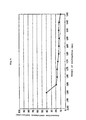
- the relationship between the amount of contraction of the compression type connector and the applied load is depicted in the graph shown in Fig.4. In this chart, the ordinate indicates the load per each conductive pin (N/pin) and the abscissa the amount of contraction (mm).
- Fig.5 shows a graph representing the relationship between the amount of contraction and connection resistance of the compression type connector.
- Fig.6 shows a graph representing the relationship between the amount of contraction and inductance of the compression type connector.
- the ordinate indicates the connection resistance (milli-ohm) and the abscissa the amount of contraction (mm).
- the ordinate indicates the inductance (nH) and the abscissa the frequency (MHz).
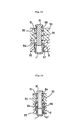
- a conductive toe-pin 1 of the compression type connector is configured so as to project out and downwards in a sliding manner. That is, conductive toe-pin 1 and conductive pin 10 are caused to project out, in the opposite directions, upwards and downwards, by the repulsive force of coil spring 20.
- This compression type connector is disposed to each of multiple passage holes 51 of a housing 50 of a multiple-layered form.
- conductive toe-pin 1 is formed of, for example, a cylinder with a bottom having an approximately U-shaped section, with gold-plated conductive material, specifically, copper, brass, aluminum or the like.
- Conductive toe-pin 1 is formed with a semispherical or conical bottom, and an annular flange 2 is formed radially outwardly on the outer periphery of the upper opening.
- conductive pin 10 is, for example, formed of a cylindrical pin made of conductive elastomer or conductive copper, brass or aluminum plated with gold.
- This conductive pin 10 is shaped so that the top face is formed with a curved surface of a semispherical shape so that this top face will come into smooth contact with electrode 41 of electrically joined object 40.
- Conductive pin 10 is arranged so that it marginally projects above the top surface of housing 50 when it is connected for conduction. The projected amount is about 0.1 to 1.5 mm or preferably 0.5 to 1.0 mm.
- housing 50 is formed of a pair of thin housing plates 55, laminated one over the other, forming a flat rectangular or plate-like structure with multiple small-diametric passage holes 51 bored and arranged lengthwise in a row with a pitch of about 0.5 mm to 1.27 mm.
- Each housing plate 55 is formed of multi-purpose engineering plastic which is excellent in heat resistance, dimensional stability, moldability and the like (for example, ABS resin, polycarbonate, polypropylene, polyethylene, etc.). Among these, ABS resin is the most suitable in view of workability and cost.
- Housing 50 has a pair of positioning pins 56 embedded at both extremes thereof so as to extend downwards and is positioned and fixed by each positioning pin 56 being fitted into an unillustrated positioning hole in electronic circuit board 30.
- each passage hole 51 is comprised of a first reduced-diameter bore 57 formed in the lower housing plate 55 and located on the electronic circuit board 30 side, a large-diametric and large-height bore 58 which is formed in the lower housing plate 55, continuously from the upper end of the first reduced-diameter bore 57 with a step therebetween, a second reduced-diameter and large-height bore 59 which is formed in the upper housing plate 55, located on the electrically joined object 40 side and ranging continuously from the upper end of large diametric bore 58 with a slight step therebetween, all being continuously formed.
- the step between the first reduced-diameter bore 57 and large-diametric bore 58 is adapted to receive flange 2 of conductive toe-pin 1. This engagement provides effective prevention of conductive toe-pin 1 descending and dislodging. Further, the bottom part of coil spring 20 fits in the boundary between large-diametric bore 58 and second reduced-diameter bore 59. This fitting provides effective prevention against displacement and dislodgment.
- the other components are the same as the preceding embodiment, so that the description is omitted.
- the compression type connector is positioned and fixed to electronic circuit board 30. Then the compression type connector is positioned and held between electronic circuit board 30 and electrically joined object 40 so that each electrode 31 of electronic circuit board 30 comes into contact with corresponding conductive toe-pin 1 while each electrode 41 of electrically joined object 40 comes into surface contact with conductive pin 10.
- electrically joined object 40 is lightly pressed against electronic circuit board 30, each coil spring 20 contracts and conductive toe-pin 1 and conductive pin 10 move upwards and downwards, closer to each other, whereby electrical conduction between electronic circuit board 30 and electrically joined object 40 can be elastically achieved by way of conductive toe-pin 1 and conductive pin 10.
- Fig.10 shows the third embodiment.
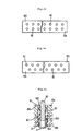
- multiple rows of small-diametric passage holes 51 arranged in the longitudinal direction of housing 50 with a predetermined pitch are formed and arrayed in a matrix, so as to mate matrix electrodes 41.
- the other components are the same as the second embodiment, so that the description is omitted.
- Fig.11 shows the fourth embodiment.
- multiple rows of small-diametric passage holes 51 arranged in the longitudinal direction of housing 50 with a predetermined pitch are formed with the multiple passage holes 51 arrayed in a staggered manner.
- the other components are the same as the second embodiment, so that the description is omitted.
- Fig.12 shows the fifth embodiment.
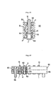
- the head of each conductive pin 10 is shaped in a conical form so that the pointed head will come into point contact with electrode 41 of electrically joined object 40 to break the oxide film over the solder of electrode 41 so as to secure good conduction.
- the other components are the same as the second embodiment, so that the description is omitted.
- Fig.13 shows the sixth embodiment.
- an upper part of each conductive pin 10 is reduced in diameter and conductive pin 10 is formed with a large-diametric obtuse conical head so that the pointed part will come into point contact with electrode 41 of electrically joined object 40 to break the oxide film over the solder of electrode 41.
- the top end of coil spring 20 is fitted to the upper part of conductive pin 10 so as to effectively prevent the pin from falling off or displacing.
- the other components are the same as the second embodiment, so that the description is omitted.
- Fig.14 shows the seventh embodiment.
- an upper part of each conductive pin 10 is reduced in diameter and conductive pin 10 is formed with a large-diametric head having a small pointed cone at the center of the flat top so that this cone will come into point contact with electrode 41 of electrically joined object 40 to break the oxide film over the solder of electrode 41.
- the top end of coil spring 20 is fitted to the upper part of conductive pin 10 so as to effectively prevent the pin from falling off or displacing.
- the other components are the same as the second embodiment, so that the description is omitted.
- Fig.15 shows the eighth embodiment.
- an upper part of each conductive pin 10 is reduced in diameter and conductive pin 10 is formed with a large-diametric crown-shaped or approximately dowel-shaped head so that the complexly jagged head will come into contact with electrode 41 of electrically joined object 40 and easily break the oxide film over the solder of electrode 41 (this configuration is especially effective in prevention against displacement for a BGA solder-ball electrode).
- the top end of coil spring 20 is fitted to the upper part of conductive pin 10 so as to effectively prevent the pin from falling off or displacing.
- the other components are the same as the second embodiment, so that the description is omitted.
- a conductive toe-pin 1 of the compression type connector is configured so as to project out and downwards in a sliding manner. That is, conductive toe-pin 1 and conductive pin 10 are caused to project out, in the opposite directions, upwards and downwards, by the repulsive force of coil spring 20. Further, an annular stopper flange 11 is formed radially outwardly from the upper part on the peripheral side of conductive pin 10, and this compression type connector is disposed to each of multiple passage holes 51 of a housing 50 of a multiple-layered form.
- the conductive pin 10 is formed so that the top face is formed with a curved surface of a semispherical shape so that this top face marginally projects above the upper surface of housing 50 (by a projected amount of about 0.1 to 1.5 mm, or preferably 0.5 to 1.0 mm) so as to come into contact with electrode 41 of electrically joined object 40, making sure of conduction.
- Coil spring 20 has a large-diametric portion at its bottom which abuts the upper end face of the opening of conductive toe-pin 1 while its upper part as a free end abuts the underside of stopper flange 11 of conductive pin 10.
- Housing 50 is formed of a pair of thin housing plates 55, laminated one over the other, forming a flat rectangular or plate-like structure with small-diametric passage holes 51 bored and arranged lengthwise in a row with a predetermined pitch.
- Each passage hole 51 is comprised of a reduced-diameter bore 60 formed in the lower housing plate 55 and located on the electronic circuit board 30 side, a large-diametric and large-height bore 61 which is formed in the housing plates 55, continuously from the upper end of the reduced-diameter bore 60 with a step therebetween, a small-diametric bore 62 which is formed in the upper housing plate 55, continuously from the upper end of the large-diametric bore 61 with a step therebetween and located on the electrically joined object 40 side, all being continuously formed.
- the step between the reduced-diameter bore 60 and large-diametric bore 61 is adapted to receive flange 2 of conductive toe-pin 1.
- This engagement provides markedly effective prevention of conductive toe-pin 1 descending and dislodging.
- the other step between the large-diametric bore 61 and small-diametric bore 62 is adapted to receive stopper flange 11 of conductive pin 10. This engagement provides effective prevention of conductive pin 10 falling off and other displacement.
- the other components are the same as the preceding embodiment, so that the description is omitted.
- Fig.19 shows the tenth embodiment.
- multiple rows of small-diametric passage holes 51 arranged in the longitudinal direction of a housing 50 with a predetermined pitch are formed and arrayed in a matrix, so as to mate matrix electrodes 41.
- the other components are the same as the ninth embodiment, so that the description is omitted.
- Fig.20 shows the eleventh embodiment.
- multiple rows of small-diametric passage holes 51 arranged in the longitudinal direction of housing 50 with a predetermined pitch are formed with the multiple passage holes 51 arrayed in a staggered manner, so as to mate matrix electrodes 41.
- the other components are the same as the ninth embodiment, so that the description is omitted.
- Fig.21 shows the twelfth embodiment.
- the head of each conductive pin 10 is shaped in a conical form so that the pointed head will come into point contact with electrode 41 of electrically joined object 40 to break the oxide film over the solder of electrode 41 so as to secure good conduction.
- the other components are the same as the ninth embodiment, so that the description is omitted.
- Fig.22 shows the thirteenth embodiment.
- each conductive pin 10 is formed with a head having a small pointed cone at the center of the flat top so that this cone will come into point contact with electrode 41 of electrically joined object 40 to break the oxide film over the solder.
- the other components are the same as the ninth embodiment, so that the description is omitted.
- Fig.23 shows the fourteenth embodiment.
- each conductive pin 10 is projectively formed with a large-diametric crown-shaped or approximately dowel-shaped head so that the jagged head will come into contact with electrode 41 of electrically joined object 40 and easily break the oxide film over the solder of electrode 41 (this configuration is especially effective in prevention against displacement for a BGA solder-ball electrode).
- the other components are the same as the ninth embodiment, so that the description is omitted.
- Figs.24 through 27 show the fifteenth embodiment.
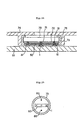
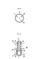
- This embodiment includes an insulative holder 73 of a cylinder with a bottom for accommodating an electroacoustic part, interposed between an electronic circuit board 30 of a cellular phone and a miniature electroacoustic part 70, one opposing the other.
- a multiple number of passage holes 51 are formed in an insulative housing 50, which is attached to the bottom part of holder 73, and a multiple number of dummy probes 80 are also formed in the holder bottom.
- a compression type connector is set in each passage hole 51.
- This compression type connector is arranged so that the bottom part of the conductive toe-pin is exposed downward from the undersurface side of the holder's bottom while conductive pin 10 of the compression type connector is projected from the obverse side of the holder's bottom toward the electroacoustic part.
- Electroacoustic part 70 may be a miniature microphone for a cellular phone, etc., for example, and has a circular electrode 71 at the center of the bottom and a doughnut electrode 72 enclosing the circular electrode 71, on the remaining peripheral part of the bottom.
- the circular electrode 71 and doughnut electrode 72 oppose the bottom of holder 73 with a clearance therebetween.
- holder 73 has an approximately U-shaped section, and is formed of a predetermined insulative elastomer and fitted to an attachment port 75 of a body case 74 of a cellular phone or the like to provide an anti-vibration function as well as an anti-howling function.
- Examples of the specific materials for this holder 73 having elastic properties include natural rubber, polyisoprene, polybutadiene, chloroprene rubber, polyurethane rubber and silicone rubber. Among these, silicone rubber is the most suitable taking into account weatherability, distortion under compression characteristics, workability and other factors.
- the bottom part of holder 73 may either be, or need not, be, formed of the aforementioned insulative elastomer.
- the bottom part of holder 73 can be formed separately, of a predetermined plastic.
- examples of the specific materials include ABS resin, polycarbonate, polypropylene and polyethylene. Among these, ABS resin is the most suitable taking into account retention of compression type connectors, workability, cost and other factors.
- a flange 76 is projected radially inwardly from the inner rim of the top opening of holder 73 so as to effectively prevent electroacoustic part 70 from dislodging.
- the housing 50 and compression type connector are much the same as those in the first and second embodiments, so that the description is omitted.
- the multiple dummy probes 80 are formed in a pin form using the same material as holder 73, and have much the same height and size as the compression type connector and function to appropriately support electroacoustic part 70 in cooperation with the compression type connectors.
- Each dummy probe 80 is integrated with the bottom part of holder 73 and put in contact with doughnut electrode 72 of electroacoustic part 70.
- the other components are the same as the preceding embodiment.
- the same effect as in the preceding embodiment can be expected. Further, since wire soldering can be omitted, it is not only possible to obviate the necessity of complicated work management, but also a low-load connection can be highly expected. Further, since electroacoustic part 70 can be held in its correct posture by means of miniature compression type connectors and dummy probes 80, electroacoustic part 70 can be prevented from being tilted or displaced, by a simple configuration. Moreover, since compression type connectors are arranged between electronic circuit board 30 and electroacoustic part 70, by means of holder 73 and housing 50, the compression type connectors can be assembled or mounted by a simple arrangement. hence it is possible to markedly improve positioning accuracy and assembly performance.
- Fig.28 shows the sixteenth embodiment.
- compression type connectors are directly arranged in the bottom of holder 73, instead of using a housing 50, in order to reduce the number of parts, and the compression type connectors and dummy probes 80 are changed in their number and layout, as shown in the drawing.
- the other components are the same as the fifteenth embodiment, so that the description is omitted.
- Fig.29 shows the seventeenth embodiment.
- the housing 50 is formed in a multiple-layered structure, and each passage hole 51 is formed as in the second embodiment so that a conductive toe-pin 1 is fitted in a slidable manner into the passage hole 51 while the head of each conductive pin 10 is curved or formed in a semispherical form and the bottom part of each coil spring 20 is made large in diameter and loosely fitted at the boundary between a large-diametric bore 58 and second reduced-diameter bore 59 of passage hole 51.
- each conductive toe-pin 1 is curved or formed in a smooth semispherical shape.
- a large-diametric flange 2 is formed in the upper part of conductive toe-pin 1 on its outer periphery. This flange 2 abuts the step between a first reduced-diameter bore 57 and large-diametric bore 58 so that it will not come off.
- This conductive toe-pin 1 is not fixed but is projected out, by the repulsive force of coil spring 20, from housing 50 of holder 73 downwards in a vertically movable manner.
- the other components are the same as in the fifteenth embodiment, so that the description is omitted.
- each passage hole 51 is formed as in the ninth embodiment.
- Each conductive pin 10 has an annular stopper flange 11 projected radially outwardly from the peripheral side at the upper part thereof while the head of the conductive pin 10 is not made large in diameter and is formed with a smooth semispherical surface.
- a coil spring 20 is formed in a cylindrical shape with its lower end and middle part loosely fitted in a large-diametric bore 61 of passage hole 51. The coil spring 20 is set so that its upper end abuts the stopper flange 11 of conducive pin 10 and the other end rests on the top outer peripheral surface of conductive toe-pin 1.
- Stopper flange 11 of conductive pin 10 abuts the step between a reduced-diameter bore 60 and large-diametric bore 61 of passage hole 51 so that it will not dislodge or come off.
- the other components are the same as in the seventeenth embodiment, so that the description is omitted.
- Fig.31 shows the nineteenth embodiment.
- the housing 50 is formed in a multiple-layered structure, and each passage hole 51 is formed as in the second embodiment so that a conductive toe-pin 1 is fitted in a slidable manner into the passage hole 51.
- the head of each conductive pin 10 is formed with a large-diametric complexly jagged or approximately tooth-shaped pin-joint dowel form, so that it will easily break the oxide film of solder plating, for example, of circular electrode 71 or doughnut electrode 72 of electroacoustic part 70.
- the bottom end of each coil spring 20 is formed to be large in diameter so that it is loosely fitted inside a large-diametric bore 58 of passage hole 51.
- the other components are the same as in the seventeenth embodiment, so that the description is omitted.
- housing 50 with passage holes 51 is united to the bottom part of holder 73, but the invention should not be limited thereto.
- the bottom part of holder 73 may be formed by fitting a housing 50 molded of a plasticresin, for example, as shown in Fig.28, andmultiple passage holes 51 may be directly formed in this bottom part.
- Housing 50 may be rectangular, or square, circular, elliptic or oval or of other shapes. Further, the fifteenth, sixteenth, seventeenth, eighteenth and nineteenth embodiments may be modified or combined appropriately.
- soldering upon connection can be omitted so that it is possible to simplify the connecting work.
Landscapes
- Coupling Device And Connection With Printed Circuit (AREA)
- Multi-Conductor Connections (AREA)
- Connections By Means Of Piercing Elements, Nuts, Or Screws (AREA)
Abstract
Description
Claims (3)
- A compression type connector comprising: a conductive toe-pin having a cap-like shape; a conductive pin fitted into the conductive toe-pin in a slidable manner; and a spring fitted on conductive pin, characterized in that the spring rests on the opening end face of the conductive toe-pin so as to urge the conductive pin in the direction opposite the bottom of the conductive-toe pin.
- A connecting structure of compression type connectors. characterized in that an insulative housing to be interposed between opposing electrodes has a multiple number of passage holes formed therein, and a compression type connector defined in Claim 1 is fitted in each passage hole in such a manner that the bottom of the conductive toe-pin of the compression type connector is projected from one side of the housing and the conductive pin of the compression type connector is projected on the other side of the housing.
- A connecting structure of compression type connectors, characterized in that an insulative holder to be interposed between opposing electrodes is formed in an approximate cylinder with a bottom and has a multiple number of passage holes formed in the bottom, and a compression type connector defined in Claim 1 is fitted in each passage hole in such a manner that the bottom of the conductive toe-pin of the compression type connector is projected from one side of the holder's bottom and the conductive pin of the compression type connector is projected on the other side of the holder's bottom, toward the open side.
Applications Claiming Priority (9)
| Application Number | Priority Date | Filing Date | Title |
|---|---|---|---|
| JP2000326524A JP2002134201A (en) | 2000-10-26 | 2000-10-26 | Pressure contact pinching type connector and its connecting structure |
| JP2000326524 | 2000-10-26 | ||
| JP2000334658 | 2000-11-01 | ||
| JP2000334658A JP2002141130A (en) | 2000-11-01 | 2000-11-01 | Pressure welding holding type connector and its connecting structure |
| JP2000354805A JP2002158053A (en) | 2000-11-21 | 2000-11-21 | Press-clamp type connector and its connection structure |
| JP2000354803 | 2000-11-21 | ||
| JP2000354803A JP2002158052A (en) | 2000-11-21 | 2000-11-21 | Press-clamp type connector and its connection structure |
| JP2000354805 | 2000-11-21 | ||
| PCT/JP2001/008708 WO2002035656A1 (en) | 2000-10-26 | 2001-10-03 | Press contact clamping connector and its connection structure |
Publications (3)
| Publication Number | Publication Date |
|---|---|
| EP1329991A1 true EP1329991A1 (en) | 2003-07-23 |
| EP1329991A4 EP1329991A4 (en) | 2006-07-26 |
| EP1329991B1 EP1329991B1 (en) | 2007-12-12 |
Family
ID=27481738
Family Applications (1)
| Application Number | Title | Priority Date | Filing Date |
|---|---|---|---|
| EP01974667A Expired - Lifetime EP1329991B1 (en) | 2000-10-26 | 2001-10-03 | Compression type connector and the connecting structure thereof |
Country Status (8)
| Country | Link |
|---|---|
| US (1) | US6908347B2 (en) |
| EP (1) | EP1329991B1 (en) |
| KR (1) | KR100562602B1 (en) |
| CN (1) | CN100557890C (en) |
| AT (1) | ATE381124T1 (en) |
| DE (1) | DE60131876T2 (en) |
| TW (1) | TW526329B (en) |
| WO (1) | WO2002035656A1 (en) |
Cited By (4)
| Publication number | Priority date | Publication date | Assignee | Title |
|---|---|---|---|---|
| WO2005034297A1 (en) * | 2003-09-30 | 2005-04-14 | Molex Incorporated | Battery connector |
| EP1530267A1 (en) * | 2003-11-07 | 2005-05-11 | Sony Ericsson Mobile Communications AB | Electronic connection device for transferring energy and data |
| EP2059063A1 (en) * | 2007-11-12 | 2009-05-13 | Panasonic Corporation | Electronic component, electronic component unit, speaker, and mobile terminal including speaker |
| EP3515762A4 (en) * | 2016-09-21 | 2020-07-08 | Systems and Software Enterprises, LLC | DISPLAY UNIT FOR A VEHICLE |
Families Citing this family (36)
| Publication number | Priority date | Publication date | Assignee | Title |
|---|---|---|---|---|
| JP2002329540A (en) * | 2001-05-01 | 2002-11-15 | Shin Etsu Polymer Co Ltd | Press-fit type connector for mobile phone and its connection structure |
| US8231414B2 (en) * | 2004-10-04 | 2012-07-31 | Gvi Technology Partners, Ltd. | Sensor interconnect system |
| US7186153B2 (en) * | 2004-10-13 | 2007-03-06 | Carrier Corporation | Side entry terminal pin |
| JP2006166065A (en) * | 2004-12-08 | 2006-06-22 | Matsushita Electric Ind Co Ltd | Microphone and microphone manufacturing method |
| US7690925B2 (en) * | 2005-02-24 | 2010-04-06 | Advanced Interconnections Corp. | Terminal assembly with pin-retaining socket |
| US7154286B1 (en) * | 2005-06-30 | 2006-12-26 | Interconnect Devices, Inc. | Dual tapered spring probe |
| US7255572B2 (en) * | 2005-08-31 | 2007-08-14 | Yokowo Co., Ltd. | Electrical connector provided with coiled spring contact |
| SG130069A1 (en) * | 2005-08-31 | 2007-03-20 | Fci Asia Technology Pte Ltd | Compression connector |
| US7147478B1 (en) * | 2005-09-21 | 2006-12-12 | Lotes Co., Ltd. | Electric element having liquid metals |
| TWM289241U (en) * | 2005-10-07 | 2006-04-01 | Lotes Co Ltd | Electric connector |
| US7300288B1 (en) * | 2006-08-21 | 2007-11-27 | Lotes Co., Ltd. | Electrical connector |
| US20080143367A1 (en) * | 2006-12-14 | 2008-06-19 | Scott Chabineau-Lovgren | Compliant electrical contact having maximized the internal spring volume |
| US7692508B2 (en) * | 2007-04-19 | 2010-04-06 | Raytheon Company | Spring loaded microwave interconnector |
| US7458826B1 (en) | 2007-08-13 | 2008-12-02 | Sony Ericsson Mobile Communications Ab | Compression connector for connecting electrical components |
| US7445461B1 (en) * | 2008-01-18 | 2008-11-04 | Hon Hai Precision Ind. Co., Ltd. | Composite electrical contact with elastic wire contact part and separate rigid part |
| JP2010060527A (en) * | 2008-09-05 | 2010-03-18 | Yokowo Co Ltd | Inspection unit equipped with contact probe for ground |
| DE102009054774A1 (en) | 2009-12-16 | 2011-07-21 | Robert Bosch GmbH, 70469 | Contact device for electrically contacting printed circuit board with electrical cable in engine control device, has component movable from open position into closed position, where area of board is contactable with lines in closed position |
| US8491315B1 (en) * | 2011-11-29 | 2013-07-23 | Plastronics Socket Partners, Ltd. | Micro via adapter socket |
| JP5354226B2 (en) * | 2012-01-17 | 2013-11-27 | Smk株式会社 | Pressure contact type connector |
| CN102913868A (en) * | 2012-10-14 | 2013-02-06 | 深圳市日上光电有限公司 | Conductive nail of light strip as well as manufacturing technique and use method |
| DE202012013208U1 (en) * | 2012-12-05 | 2015-06-17 | Abb Ag | Flush-mounted socket with socket pot |
| US9674943B2 (en) | 2012-12-06 | 2017-06-06 | Intel Corporation | Actuation mechanisms for electrical interconnections |
| JP6107234B2 (en) * | 2013-03-01 | 2017-04-05 | 山一電機株式会社 | Inspection probe and IC socket including the same |
| CN103794944A (en) * | 2014-01-07 | 2014-05-14 | 清华大学 | One-way operated fast socket device |
| CN103926432B (en) * | 2014-05-08 | 2016-07-06 | 威海市天罡仪表股份有限公司 | Four-wire system resistance measurement positioner |
| US9729791B2 (en) * | 2014-10-31 | 2017-08-08 | Ubiquiti Networks, Inc. | Micro camera and multi-purpose mounting base |
| US9979128B2 (en) * | 2015-02-12 | 2018-05-22 | Cisco Technology, Inc. | Radial centering mechanism for floating connection devices |
| CN105004958B (en) * | 2015-08-11 | 2018-05-04 | 太仓市高泰机械有限公司 | A kind of detecting device for thermistor |
| US9692147B1 (en) * | 2015-12-22 | 2017-06-27 | Intel Corporation | Small form factor sockets and connectors |
| CN105449412B (en) * | 2015-12-29 | 2018-07-31 | 深圳量子防务在线科技有限公司 | A kind of insulator foot and oxygen generator with scalability contact |
| CN108737916B (en) * | 2017-04-21 | 2022-03-18 | 法雷奥汽车内部控制(深圳)有限公司 | Microphone assembly for a motor vehicle |
| CN107951483B (en) * | 2017-11-21 | 2025-01-03 | 阿木(深圳)新科技有限公司 | ECG monitoring electrodes and signal acquisition tops |
| CN111146169B (en) * | 2018-11-06 | 2022-03-18 | 株洲中车时代半导体有限公司 | Conductive disc spring assembly for crimping module |
| DE102020206586A1 (en) | 2020-05-27 | 2021-12-02 | Robert Bosch Gesellschaft mit beschränkter Haftung | Contact, circuit board with the contact, and guide carriage with the circuit board for routing |
| CN112083200A (en) * | 2020-09-11 | 2020-12-15 | 苏州韬盛电子科技有限公司 | Novel high-frequency test socket |
| CN114400479A (en) * | 2022-01-12 | 2022-04-26 | 广州极飞科技股份有限公司 | Battery connector male end and female end and battery connector, battery and flight equipment |
Family Cites Families (15)
| Publication number | Priority date | Publication date | Assignee | Title |
|---|---|---|---|---|
| US3378810A (en) * | 1966-05-13 | 1968-04-16 | Amphenol Corp | Self-cleaning electrical connector |
| US5127837A (en) * | 1989-06-09 | 1992-07-07 | Labinal Components And Systems, Inc. | Electrical connectors and IC chip tester embodying same |
| JPH0412483A (en) * | 1990-04-27 | 1992-01-17 | Kel Corp | Ic socket |
| JPH06168756A (en) * | 1992-11-30 | 1994-06-14 | Nec Kansai Ltd | Contact pin |
| US5518410A (en) * | 1993-05-24 | 1996-05-21 | Enplas Corporation | Contact pin device for IC sockets |
| JP3039595B2 (en) | 1993-12-10 | 2000-05-08 | 株式会社ヨコオ | Connector pin for electrical connection |
| JP2648120B2 (en) * | 1995-02-08 | 1997-08-27 | 山一電機株式会社 | Surface contact type connector |
| US6046597A (en) * | 1995-10-04 | 2000-04-04 | Oz Technologies, Inc. | Test socket for an IC device |
| US5641315A (en) * | 1995-11-16 | 1997-06-24 | Everett Charles Technologies, Inc. | Telescoping spring probe |
| JPH10189111A (en) | 1996-12-25 | 1998-07-21 | Sony Corp | Spring contact device |
| DE69700120T2 (en) * | 1997-02-04 | 1999-10-28 | Durtal S.A., Delemont | Spring contact element |
| JP2003526874A (en) | 1998-11-25 | 2003-09-09 | リカ エレクトロニクス インターナショナル インコーポレイテッド | Electric contact device |
| US6464511B1 (en) * | 1999-11-17 | 2002-10-15 | Advantest Corporation | IC socket and IC tester |
| TW549662U (en) * | 2001-06-08 | 2003-08-21 | Hon Hai Prec Ind Co Ltd | Electrical connector |
| US6769919B2 (en) * | 2002-09-04 | 2004-08-03 | Itt Manufacturing Enterprises, Inc. | Low profile and low resistance connector |
-
2001
- 2001-10-03 KR KR1020037005747A patent/KR100562602B1/en not_active Expired - Fee Related
- 2001-10-03 DE DE60131876T patent/DE60131876T2/en not_active Expired - Lifetime
- 2001-10-03 US US10/381,078 patent/US6908347B2/en not_active Expired - Fee Related
- 2001-10-03 EP EP01974667A patent/EP1329991B1/en not_active Expired - Lifetime
- 2001-10-03 WO PCT/JP2001/008708 patent/WO2002035656A1/en not_active Ceased
- 2001-10-03 AT AT01974667T patent/ATE381124T1/en not_active IP Right Cessation
- 2001-10-03 CN CNB018180221A patent/CN100557890C/en not_active Expired - Fee Related
- 2001-10-19 TW TW090125947A patent/TW526329B/en not_active IP Right Cessation
Cited By (4)
| Publication number | Priority date | Publication date | Assignee | Title |
|---|---|---|---|---|
| WO2005034297A1 (en) * | 2003-09-30 | 2005-04-14 | Molex Incorporated | Battery connector |
| EP1530267A1 (en) * | 2003-11-07 | 2005-05-11 | Sony Ericsson Mobile Communications AB | Electronic connection device for transferring energy and data |
| EP2059063A1 (en) * | 2007-11-12 | 2009-05-13 | Panasonic Corporation | Electronic component, electronic component unit, speaker, and mobile terminal including speaker |
| EP3515762A4 (en) * | 2016-09-21 | 2020-07-08 | Systems and Software Enterprises, LLC | DISPLAY UNIT FOR A VEHICLE |
Also Published As
| Publication number | Publication date |
|---|---|
| CN1471751A (en) | 2004-01-28 |
| US20030190825A1 (en) | 2003-10-09 |
| EP1329991A4 (en) | 2006-07-26 |
| EP1329991B1 (en) | 2007-12-12 |
| ATE381124T1 (en) | 2007-12-15 |
| CN100557890C (en) | 2009-11-04 |
| WO2002035656A1 (en) | 2002-05-02 |
| KR100562602B1 (en) | 2006-03-17 |
| DE60131876D1 (en) | 2008-01-24 |
| TW526329B (en) | 2003-04-01 |
| DE60131876T2 (en) | 2008-12-04 |
| KR20030048079A (en) | 2003-06-18 |
| US6908347B2 (en) | 2005-06-21 |
Similar Documents
| Publication | Publication Date | Title |
|---|---|---|
| US6908347B2 (en) | Compression type connector and the connecting structure thereof | |
| EP1326308B1 (en) | Spring element, press-clamped connector, and holder with probe for electro-acoustic component | |
| JP4037434B2 (en) | Press-clamping connector | |
| KR101974811B1 (en) | Integrated pogo pin capable of sigle body housing | |
| CN114502965B (en) | Spring contact and built-in test socket of spring contact | |
| JPH10214649A (en) | Spring connector and device using spring connector | |
| US5816828A (en) | Socket | |
| US11162979B2 (en) | Plate spring-type connecting pin | |
| JP2002100431A (en) | Pressure contact connector | |
| US20040166701A1 (en) | Mechanical-contact adapter | |
| NO327109B1 (en) | Pressure type connector and its coupling structure | |
| CN1319217C (en) | Pressure contact connector of cell phone and connection structure of the connector | |
| EP1394905A1 (en) | CONNECTOR FOR ELECTRO−ACOUSTIC COMPONENT AND CONNECTION STRUCTURE THEREOF | |
| CN111293448B (en) | Integrated spring needle with pressure welding structure | |
| JP2002158053A (en) | Press-clamp type connector and its connection structure | |
| JP3194708B2 (en) | Socket for IC | |
| JP2002141130A (en) | Pressure welding holding type connector and its connecting structure | |
| JP3007244U (en) | Flexible wiring board connection structure | |
| JP2004047330A (en) | Crimp holding type connector and its connection structure | |
| JP2002158052A (en) | Press-clamp type connector and its connection structure | |
| JP2002117925A (en) | Vibrator with connector | |
| JPH10163384A (en) | Socket and method for mounting semiconductor package | |
| JP2002159913A (en) | Vibrator with connector and its connecting structure | |
| JP2002112375A (en) | Holder for electroacoustic component with probe | |
| JP2002373716A (en) | Elastic connector for vibration generator and device fitted therewith |
Legal Events
| Date | Code | Title | Description |
|---|---|---|---|
| PUAI | Public reference made under article 153(3) epc to a published international application that has entered the european phase |
Free format text: ORIGINAL CODE: 0009012 |
|
| 17P | Request for examination filed |
Effective date: 20030320 |
|
| AK | Designated contracting states |
Designated state(s): AT BE CH CY DE DK ES FI FR GB GR IE IT LI LU MC NL PT SE TR |
|
| A4 | Supplementary search report drawn up and despatched |
Effective date: 20060627 |
|
| RIC1 | Information provided on ipc code assigned before grant |
Ipc: H01R 12/16 20060101ALI20060621BHEP Ipc: H01R 13/24 20060101AFI20020504BHEP Ipc: H01R 12/22 20060101ALI20060621BHEP |
|
| 17Q | First examination report despatched |
Effective date: 20061024 |
|
| GRAP | Despatch of communication of intention to grant a patent |
Free format text: ORIGINAL CODE: EPIDOSNIGR1 |
|
| GRAS | Grant fee paid |
Free format text: ORIGINAL CODE: EPIDOSNIGR3 |
|
| GRAA | (expected) grant |
Free format text: ORIGINAL CODE: 0009210 |
|
| RTI1 | Title (correction) |
Free format text: COMPRESSION TYPE CONNECTOR AND THE CONNECTING STRUCTURE THEREOF |
|
| AK | Designated contracting states |
Kind code of ref document: B1 Designated state(s): AT BE CH CY DE DK ES FI FR GB GR IE IT LI LU MC NL PT SE TR |
|
| REG | Reference to a national code |
Ref country code: GB Ref legal event code: FG4D |
|
| REG | Reference to a national code |
Ref country code: CH Ref legal event code: EP |
|
| REG | Reference to a national code |
Ref country code: IE Ref legal event code: FG4D |
|
| REF | Corresponds to: |
Ref document number: 60131876 Country of ref document: DE Date of ref document: 20080124 Kind code of ref document: P |
|
| REG | Reference to a national code |
Ref country code: SE Ref legal event code: TRGR |
|
| PG25 | Lapsed in a contracting state [announced via postgrant information from national office to epo] |
Ref country code: CH Free format text: LAPSE BECAUSE OF FAILURE TO SUBMIT A TRANSLATION OF THE DESCRIPTION OR TO PAY THE FEE WITHIN THE PRESCRIBED TIME-LIMIT Effective date: 20071212 Ref country code: LI Free format text: LAPSE BECAUSE OF FAILURE TO SUBMIT A TRANSLATION OF THE DESCRIPTION OR TO PAY THE FEE WITHIN THE PRESCRIBED TIME-LIMIT Effective date: 20071212 |
|
| REG | Reference to a national code |
Ref country code: CH Ref legal event code: PL |
|
| PG25 | Lapsed in a contracting state [announced via postgrant information from national office to epo] |
Ref country code: AT Free format text: LAPSE BECAUSE OF FAILURE TO SUBMIT A TRANSLATION OF THE DESCRIPTION OR TO PAY THE FEE WITHIN THE PRESCRIBED TIME-LIMIT Effective date: 20071212 |
|
| PG25 | Lapsed in a contracting state [announced via postgrant information from national office to epo] |
Ref country code: ES Free format text: LAPSE BECAUSE OF FAILURE TO SUBMIT A TRANSLATION OF THE DESCRIPTION OR TO PAY THE FEE WITHIN THE PRESCRIBED TIME-LIMIT Effective date: 20080323 |
|
| ET | Fr: translation filed | ||
| PG25 | Lapsed in a contracting state [announced via postgrant information from national office to epo] |
Ref country code: BE Free format text: LAPSE BECAUSE OF FAILURE TO SUBMIT A TRANSLATION OF THE DESCRIPTION OR TO PAY THE FEE WITHIN THE PRESCRIBED TIME-LIMIT Effective date: 20071212 |
|
| PG25 | Lapsed in a contracting state [announced via postgrant information from national office to epo] |
Ref country code: PT Free format text: LAPSE BECAUSE OF FAILURE TO SUBMIT A TRANSLATION OF THE DESCRIPTION OR TO PAY THE FEE WITHIN THE PRESCRIBED TIME-LIMIT Effective date: 20080512 |
|
| PLBE | No opposition filed within time limit |
Free format text: ORIGINAL CODE: 0009261 |
|
| STAA | Information on the status of an ep patent application or granted ep patent |
Free format text: STATUS: NO OPPOSITION FILED WITHIN TIME LIMIT |
|
| PG25 | Lapsed in a contracting state [announced via postgrant information from national office to epo] |
Ref country code: DK Free format text: LAPSE BECAUSE OF FAILURE TO SUBMIT A TRANSLATION OF THE DESCRIPTION OR TO PAY THE FEE WITHIN THE PRESCRIBED TIME-LIMIT Effective date: 20071212 |
|
| 26N | No opposition filed |
Effective date: 20080915 |
|
| PG25 | Lapsed in a contracting state [announced via postgrant information from national office to epo] |
Ref country code: GR Free format text: LAPSE BECAUSE OF FAILURE TO SUBMIT A TRANSLATION OF THE DESCRIPTION OR TO PAY THE FEE WITHIN THE PRESCRIBED TIME-LIMIT Effective date: 20080313 |
|
| PG25 | Lapsed in a contracting state [announced via postgrant information from national office to epo] |
Ref country code: MC Free format text: LAPSE BECAUSE OF NON-PAYMENT OF DUE FEES Effective date: 20081031 |
|
| PG25 | Lapsed in a contracting state [announced via postgrant information from national office to epo] |
Ref country code: CY Free format text: LAPSE BECAUSE OF FAILURE TO SUBMIT A TRANSLATION OF THE DESCRIPTION OR TO PAY THE FEE WITHIN THE PRESCRIBED TIME-LIMIT Effective date: 20071212 |
|
| PG25 | Lapsed in a contracting state [announced via postgrant information from national office to epo] |
Ref country code: IE Free format text: LAPSE BECAUSE OF NON-PAYMENT OF DUE FEES Effective date: 20081003 |
|
| PGFP | Annual fee paid to national office [announced via postgrant information from national office to epo] |
Ref country code: GB Payment date: 20090930 Year of fee payment: 9 |
|
| PGFP | Annual fee paid to national office [announced via postgrant information from national office to epo] |
Ref country code: DE Payment date: 20091001 Year of fee payment: 9 Ref country code: FI Payment date: 20091014 Year of fee payment: 9 Ref country code: SE Payment date: 20091007 Year of fee payment: 9 |
|
| PGFP | Annual fee paid to national office [announced via postgrant information from national office to epo] |
Ref country code: NL Payment date: 20091015 Year of fee payment: 9 |
|
| PGFP | Annual fee paid to national office [announced via postgrant information from national office to epo] |
Ref country code: FR Payment date: 20091029 Year of fee payment: 9 Ref country code: IT Payment date: 20091016 Year of fee payment: 9 |
|
| PG25 | Lapsed in a contracting state [announced via postgrant information from national office to epo] |
Ref country code: LU Free format text: LAPSE BECAUSE OF NON-PAYMENT OF DUE FEES Effective date: 20081003 |
|
| PG25 | Lapsed in a contracting state [announced via postgrant information from national office to epo] |
Ref country code: TR Free format text: LAPSE BECAUSE OF FAILURE TO SUBMIT A TRANSLATION OF THE DESCRIPTION OR TO PAY THE FEE WITHIN THE PRESCRIBED TIME-LIMIT Effective date: 20071212 |
|
| REG | Reference to a national code |
Ref country code: NL Ref legal event code: V1 Effective date: 20110501 |
|
| GBPC | Gb: european patent ceased through non-payment of renewal fee |
Effective date: 20101003 |
|
| PG25 | Lapsed in a contracting state [announced via postgrant information from national office to epo] |
Ref country code: FR Free format text: LAPSE BECAUSE OF NON-PAYMENT OF DUE FEES Effective date: 20101102 |
|
| REG | Reference to a national code |
Ref country code: FR Ref legal event code: ST Effective date: 20110630 |
|
| PG25 | Lapsed in a contracting state [announced via postgrant information from national office to epo] |
Ref country code: NL Free format text: LAPSE BECAUSE OF NON-PAYMENT OF DUE FEES Effective date: 20110501 Ref country code: GB Free format text: LAPSE BECAUSE OF NON-PAYMENT OF DUE FEES Effective date: 20101003 Ref country code: FI Free format text: LAPSE BECAUSE OF NON-PAYMENT OF DUE FEES Effective date: 20101003 |
|
| REG | Reference to a national code |
Ref country code: DE Ref legal event code: R119 Ref document number: 60131876 Country of ref document: DE Effective date: 20110502 |
|
| PG25 | Lapsed in a contracting state [announced via postgrant information from national office to epo] |
Ref country code: SE Free format text: LAPSE BECAUSE OF NON-PAYMENT OF DUE FEES Effective date: 20101004 |
|
| PG25 | Lapsed in a contracting state [announced via postgrant information from national office to epo] |
Ref country code: IT Free format text: LAPSE BECAUSE OF NON-PAYMENT OF DUE FEES Effective date: 20101003 |
|
| PG25 | Lapsed in a contracting state [announced via postgrant information from national office to epo] |
Ref country code: DE Free format text: LAPSE BECAUSE OF NON-PAYMENT OF DUE FEES Effective date: 20110502 |