EP1327997A2 - Elastic sheet structure having an improved electrical continuity function, and printed circuit board structure - Google Patents
Elastic sheet structure having an improved electrical continuity function, and printed circuit board structure Download PDFInfo
- Publication number
- EP1327997A2 EP1327997A2 EP03000560A EP03000560A EP1327997A2 EP 1327997 A2 EP1327997 A2 EP 1327997A2 EP 03000560 A EP03000560 A EP 03000560A EP 03000560 A EP03000560 A EP 03000560A EP 1327997 A2 EP1327997 A2 EP 1327997A2
- Authority
- EP
- European Patent Office
- Prior art keywords
- continuity
- circuit board
- printed circuit
- elastic sheet
- members
- Prior art date
- Legal status (The legal status is an assumption and is not a legal conclusion. Google has not performed a legal analysis and makes no representation as to the accuracy of the status listed.)
- Granted
Links
- 239000012811 non-conductive material Substances 0.000 claims abstract description 12
- 239000004020 conductor Substances 0.000 claims description 12
- 229920001971 elastomer Polymers 0.000 abstract description 39
- 229920002379 silicone rubber Polymers 0.000 abstract description 35
- 230000000694 effects Effects 0.000 description 14
- 238000000034 method Methods 0.000 description 7
- 230000005489 elastic deformation Effects 0.000 description 4
- 238000004519 manufacturing process Methods 0.000 description 4
- 238000005452 bending Methods 0.000 description 2
- 239000013013 elastic material Substances 0.000 description 2
- 239000007787 solid Substances 0.000 description 2
- 238000006073 displacement reaction Methods 0.000 description 1
- 239000000463 material Substances 0.000 description 1
- 230000002093 peripheral effect Effects 0.000 description 1
- 239000011347 resin Substances 0.000 description 1
- 229920005989 resin Polymers 0.000 description 1
- 238000007493 shaping process Methods 0.000 description 1
- 239000000758 substrate Substances 0.000 description 1
Images




Classifications
-
- H—ELECTRICITY
- H01—ELECTRIC ELEMENTS
- H01H—ELECTRIC SWITCHES; RELAYS; SELECTORS; EMERGENCY PROTECTIVE DEVICES
- H01H13/00—Switches having rectilinearly-movable operating part or parts adapted for pushing or pulling in one direction only, e.g. push-button switch
- H01H13/70—Switches having rectilinearly-movable operating part or parts adapted for pushing or pulling in one direction only, e.g. push-button switch having a plurality of operating members associated with different sets of contacts, e.g. keyboard
- H01H13/78—Switches having rectilinearly-movable operating part or parts adapted for pushing or pulling in one direction only, e.g. push-button switch having a plurality of operating members associated with different sets of contacts, e.g. keyboard characterised by the contacts or the contact sites
- H01H13/80—Switches having rectilinearly-movable operating part or parts adapted for pushing or pulling in one direction only, e.g. push-button switch having a plurality of operating members associated with different sets of contacts, e.g. keyboard characterised by the contacts or the contact sites characterised by the manner of cooperation of the contacts, e.g. with both contacts movable or with bounceless contacts
-
- H—ELECTRICITY
- H01—ELECTRIC ELEMENTS
- H01H—ELECTRIC SWITCHES; RELAYS; SELECTORS; EMERGENCY PROTECTIVE DEVICES
- H01H13/00—Switches having rectilinearly-movable operating part or parts adapted for pushing or pulling in one direction only, e.g. push-button switch
- H01H13/70—Switches having rectilinearly-movable operating part or parts adapted for pushing or pulling in one direction only, e.g. push-button switch having a plurality of operating members associated with different sets of contacts, e.g. keyboard
- H01H13/702—Switches having rectilinearly-movable operating part or parts adapted for pushing or pulling in one direction only, e.g. push-button switch having a plurality of operating members associated with different sets of contacts, e.g. keyboard with contacts carried by or formed from layers in a multilayer structure, e.g. membrane switches
-
- H—ELECTRICITY
- H01—ELECTRIC ELEMENTS
- H01H—ELECTRIC SWITCHES; RELAYS; SELECTORS; EMERGENCY PROTECTIVE DEVICES
- H01H2201/00—Contacts
- H01H2201/008—Both contacts movable
-
- H—ELECTRICITY
- H01—ELECTRIC ELEMENTS
- H01H—ELECTRIC SWITCHES; RELAYS; SELECTORS; EMERGENCY PROTECTIVE DEVICES
- H01H2205/00—Movable contacts
- H01H2205/002—Movable contacts fixed to operating part
-
- H—ELECTRICITY
- H01—ELECTRIC ELEMENTS
- H01H—ELECTRIC SWITCHES; RELAYS; SELECTORS; EMERGENCY PROTECTIVE DEVICES
- H01H2209/00—Layers
- H01H2209/024—Properties of the substrate
- H01H2209/03—Properties of the substrate elastomeric
Definitions
- the present invention relates to an elastic sheet structure having an electrical continuity function and to a printed circuit board structure.
- a conventional printed circuit board structure is illustrated in Fig. 9.
- a plurality of rubber contacts 102 each having an On/Off switching function moderated by elastic deformation are formed integrally at predetermined positions of a silicon rubber sheet 100.
- a movable contact 104 is fixed to the reverse surface of each rubber contact 102.
- a printed circuit board (PCB) 110 at which fixed contacts 106, a connector 108, and the like are assembled, is disposed at the reverse surface side of the silicon rubber sheet 100.
- a widthwise direction dimension P of the printed circuit board 110 is set to be substantially the same as a widthwise direction dimension Q of the silicon rubber sheet 100.
- the rubber contact 102 when the rubber contact 102 provided at the silicon rubber sheet 100 is pressed, the rubber contact 102 elastically deforms and sinks in, such that the movable contact 104 is displaced in the direction of pushing and is set in a state of being electrically continuous with the fixed contact 106.
- the above-described conventional printed circuit board structure is structured from the standpoint that only a contact function and an On/Off switching function moderated by elastic deformation are required of the silicon rubber sheet 100, and electrical flow continuity between the rubber contacts 102 is ensured separately at the printed circuit board 110. Therefore, the printed circuit board 110 must be of a size such that the printed circuit board 110 can cover at least the range over which all of the rubber contacts 102 are disposed as seen in plan view. Thus, the printed circuit board 110 is made large, and consequently, the space required for placement of the printed circuit board 110 also is large. As a result, disadvantages such as a decrease in the number of degrees of freedom in design, and increases in the size, weight and cost of the manufactured product arise.
- an object of the present invention is to provide an elastic sheet structure having an improved electrical continuity function and a printed circuit board structure in which the number of degrees of freedom in design can be increased, and which can be made smaller-sized, lighter-weight, and lower-cost.
- an elastic sheet structure having an (improved) electrical continuity function comprises: an elastic sheet member formed of a non-conductive material and formed in a sheet-shaped form, and having push portions which, when pushed, elastically deform and displace movable contacts, which are provided at reverse surface sides of the push portions, in a direction of pushing by a predetermined distance so as to make the movable contacts electrically continuous with fixed contacts; and continuity members provided at the elastic sheet member and formed of a conductive material and formed in a wire-like pattern, starting end portions of the continuity members being connected to the movable contacts or the fixed contacts, and final end portions of the continuity members being exposed to an exterior of the elastic sheet member for connection to a printed circuit board which is provided separately and independently at a reverse surface side of the elastic sheet member.
- the starting end portions of the continuity members of the above-described elastic sheet structure having an improved electrical continuity function are disposed so as to be dispersed at optional plural places in accordance with places at which the push portions are set, and the final end portions of the continuity members are disposed intensively at a small number of specific places.
- a printed circuit board structure comprises: an elastic sheet member formed of a non-conductive material and formed in a sheet-shaped form, and having push portions which, when pushed, elastically deform and displace movable contacts, which are provided at reverse surface sides of the push portions, in a direction of pushing by a predetermined distance so as to make the movable contacts electrically continuous with fixed contacts; a printed circuit board fixed to a reverse surface side of the elastic sheet member; and continuity members formed of a conductive material and formed in a wire-like pattern, starting end portions of the continuity members being connected to the movable contacts or the fixed contacts, and final end portions of the continuity members being connected to the printed circuit board.
- the starting end portions of the continuity members of the above-described printed circuit board structure are disposed so as to be dispersed at optional plural places in accordance with places at which the push portions are set, and the final end portions of the continuity members are disposed intensively at a small number of specific places.
- the movable contacts provided at the rear surface thereof are displaced in the direction of pushing by a predetermined distance, and become electrically continuous with the fixed contacts.
- the starting end portions of the continuity members are connected to the movable contacts or the fixed contacts of the elastic sheet member.
- the final end portions of the continuity members are exposed to the exterior of the elastic sheet member, in order to be connected to a printed circuit board which is provided independent and separately at the reverse surface side of the elastic sheet member. Accordingly, as a result of the above-described operation, electric flow continuity paths are ensured.
- the continuity members which are formed of a conductive material and are formed in a wire-like pattern (this "a wire-like pattern” includes a complicated a net-work like pattern, too), are provided at the elastic sheet member, which is formed of a non-conductive material and is formed in a sheet-shaped form.
- the final end portions of the continuity members are connected to the printed circuit board.
- the functions of the printed circuit board can be simplified as a whole.
- the printed circuit board can be made compact, and the space required for placement thereof can be reduced. In this way, the degrees of freedom in design can be increased, and a manufactured product can be made compact and lighter weight. This leads to a reduction in manufacturing costs as well.
- the starting end portions of the continuity members are disposed so as to be dispersed at optional plural places in accordance with places at which the push portions are set, and the final end portions of the continuity members are disposed intensively at a small number of specific places. Accordingly, in accordance with the present aspect, no matter how many plural places the push portions are dispersed at, it suffices for the printed circuit board itself to exist at a range which can cover the small number of specific places where the final end portions of the continuity members are disposed. Accordingly, the more pushing members that are provided, the more effective is the present invention.
- a printed circuit board structure is formed to include a printed circuit board and the elastic sheet member having an improved electrical continuity function based on the first aspect.
- the elastic sheet structure having an improved electrical continuity function based on the first aspect is directly applied in the present aspect, the above-described excellent effects based on the first aspect can similarly be obtained in the present aspect. Accordingly, in the present aspect as well, the printed circuit board can be made compact, and the space required for placement thereof can be reduced. In this way, the degrees of freedom in design can be increased, and a manufactured product can be made compact and lighter weight. This leads to a reduction in manufacturing costs as well.
- a printed circuit board structure is formed to include a printed circuit board and the elastic sheet member having an improved electrical continuity function based on the second aspect.
- the elastic sheet structure having an improved electrical continuity function based on the second aspect is directly applied in the present aspect, the above-described excellent effects based on the second aspect can similarly be obtained in the present aspect. Accordingly, in the printed circuit board structure, the printed circuit board can be made compact, and the space required for placement thereof can be reduced. In this way, the degrees of freedom in design of the printed circuit board structure can be increased, and a manufactured product can be made compact and lighter weight. This leads to a reduction in manufacturing costs as well.
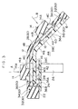
- FIG. 1 A plan view of a silicon rubber sheet relating to the present embodiment is shown in Fig. 1.
- Fig. 2 A state in which the silicon rubber sheet is made integral with a printed circuit board is shown in longitudinal sectional view in Fig. 2.
- a silicon rubber sheet 10 serving as an "elastic sheet member” has a sheet main body portion 12 which is rectangular in plan view.
- Rubber contacts 14 serving as “push portions”, which are formed as substantially T-shaped blocks in longitudinal sectional view, are formed integrally with the obverse surface side of the sheet main body portion 12. Accordingly, the rubber contacts 14 are formed of the same material as the sheet main body portion 12 (i.e., the rubber contacts 14 are formed of a non-conductive and elastic material) . Note that, in the present embodiment, a total of six rubber contacts 14 are disposed in a grid-like form.
- the rubber contact 14 is formed by an upper portion 14A which is formed as a compressed solid cylinder, a lower portion 14B which, in the same way as the upper portion 14A, is formed as a compressed solid cylinder, and a supporting portion 14C which is skirt-shaped and which is connected to the outer peripheral lower edge of the upper portion 14A and the obverse surface of the sheet main body 12 and which is elastically deformable.
- the upper portion 14A, the lower portion 14B and the supporting portion 14C are all formed integrally with the sheet main body portion 12.
- the upper portion 14A is the portion which receives pushing force (operating force) in the direction of arrows A in Fig. 2.
- the lower portion 14B is formed to have a smaller diameter than that of the upper portion 14A, and is the portion which pushes down movable contacts (starting end portions 32A, 34A, 36A, and 38A through 38C of a wire group 30) which will be described later.
- the rubber contact 14 is raised up at the position at which the cavity is formed and supported above the cavity.
- a plate-shaped concave portion 18 is formed in the reverse surface side of the sheet main body portion 12 of the silicon rubber sheet 10.
- the fixed member 20 is formed as a resin substrate, and functions as a supporting member which supports the silicon rubber sheet 10 which is formed by an elastic material. Note that, by mounting the fixed member 20 in the concave portion 18, the cavities 16 are closed.
- a printed circuit board mounting portion 22 which projects in the direction opposite the rubber contacts 14, is formed integrally with the reverse surface of a side portion of the sheet main body portion 12 of the silicon rubber sheet 10. Accordingly, only this region at which the printed circuit board mounting portion 22 is formed is formed to be thicker than the other regions.
- a printed circuit board (PCB) 24 whose widthwise direction dimension P' (see Fig. 2) is extremely small, is mounted to the bottom surface of the printed circuit board mounting portion 22 in a state in which the printed circuit board 24 is supported in a cantilevered manner.
- a connector 26 is mounted to the printed circuit board 24, and in addition, various circuit devices 28 are mounted to the printed circuit board 24.
- the wire group 30 which serves as "(electric flow) continuity members" and which is formed of a conductive material, is disposed in a grid-like form at the sheet main body portion 12 of the silicon rubber sheet 10.
- the "wire-like pattern" of the wire group 30 may be a complicated a net-work like pattern.
- the rubber contacts 14 are disposed in two rows, and a total of six rubber contacts 14 are provided. Therefore, the wire group 30 is formed by a total of six outer wires 32, 34, 36 arranged as pairs at the left and the right, and a total of one inner wire 38 which forks off laterally at the positions at which the rubber contacts 14 are respectively formed.
- the wire group 30 is embedded in an intermediate portion in the direction of plate thickness of the sheet main body portion 12 (a method of laying out the wires in an intermediate portion).
- the starting end portions 32A, 34A, 36A of the outer wires 32, 34, 36 are formed in the shapes of semicircular plates, and are disposed so as to abut the bottom surfaces of the bottom portions 14B of the corresponding rubber contacts 14.
- Final end portions 32B, 34B, 36B of the outer wires 32, 34, 36 are disposed intensively at one place (i.e., at one corner of the rubber sheet 10 which is a portion where the printed circuit board mounting portion 22 is formed).
- the starting end portions 38A, 38B, 38C of the inner wire 38 similarly are formed in shapes of semicircular plates and disposed so as to abut the bottom surfaces of the bottom portions 14B of the corresponding rubber contacts 14.
- the starting end portions 32A, 34A, 36A of the outer wires 32, 34, 36 and the starting end portions 38A, 38B, 38C of the inner wire 38 are all portions corresponding to the "starting end portions of the continuity members" in the present invention, and are all portions functioning as "movable contacts”.
- predetermined contact gaps 40 are formed between the starting end portions 32A, 34A, 36A of the outer wires 32, 34, 36 and the starting end portions 38A, 38B, 38C of the inner wire 38.
- a final end portion 38D of the inner wire 38 is disposed between the group of final end portions (32B, 34B, 36B) of the left side outer wires 32, 34, 36 and the group of final end portions (32B, 34B, 36B) of the right side outer wires 32, 34, 36. Accordingly, all of the final end portions 32B, 34B, 36B of the outer wires 32, 34, 36 and the final end portion 38D of the inner wire 38 are disposed intensively at one place (a corner portion) of the sheet main body portion 12 of the silicon rubber sheet 10. Note that the "small number of specific places" of the present invention as recited in claims 2 and 4 means, in terms of the present embodiment, the aforementioned "one place at a corner portion of the sheet main body portion 12".
- the final end portions 32B, 34B, 36B of the outer wires 32, 34, 36 and the final end portion 38D of the inner wire 38 are connected to predetermined positions of the printed circuit board 24. In this way, the electrically continuous state of the wire group 30, which is embedded within the silicon rubber sheet 10, and the printed circuit board 24 is maintained.
- Fixed contacts 42 which serve as "fixed contacts” formed of a conductive material, are disposed at predetermined positions of the top surface of the fixed member 20 (i.e., positions opposing the bottom portions 14B of the rubber contacts 14).
- the wire group 30, which is formed of a conductive material and which is formed in the form of wires, is embedded within the silicon rubber sheet 10 which is formed of a non-conductive material and is formed in the form of a sheet, and the final end portions 32B, 34B, 36B, 38D of the wire group 30 are connected to the printed circuit board 24. Therefore, there is no need to make the printed circuit board 24 be of a size which can cover the range over which all of the rubber contacts 14 are provided.
- the printed circuit board 24 by transferring the function of the wire group 30 (i.e., the electrical flow continuity path), from being conventionally provided at the printed circuit board 24 to being provided at the silicon rubber sheet 10 formed basically of a non-conductive material, it is possible to simplify the functions demanded of the printed circuit board 24. Accordingly, in accordance with the present embodiment, it suffices for the printed circuit board 24 to be able to cover only the regions of connection with the final end portions 32B, 34B, 36B, 38D of the wire group 30. Thus, the printed circuit board 24 can be made more compact, and the space required for the placement thereof can be reduced. Namely, in the present embodiment, it suffices for the widthwise direction dimension of the printed circuit board 24 to be P' (see Fig. 2) which is half or less of the widthwise direction dimension P (see Fig. 8) of the conventional printed circuit board 110.
- the degrees of freedom in design can be increased, and a manufactured product can be made more compact and more light-weight. Moreover, the manufacturing costs can be reduced.
- the rubber contacts 14 of the silicon rubber sheet 10 are disposed so as to exist at a total of six points (places) .
- the final end portions 32B, 34B, 36B, 38D of the wire group 30 are disposed intensively at one place at a corner portion of the silicon rubber sheet 10, it suffices for the printed circuit board 24 itself to exist at a range which can cover the specific one place where the final end portions 32B, 34B, 36B, 38D of the wire group 30 are disposed.
- the more the number of rubber contacts 14 is increased the more evident are the effect of making the printed circuit board 24 compact and the accompanying effect of reducing the space required for placement of the printed circuit board 24.
- a side space 44 at the side of the printed circuit board 24, which side space 44 was what is called “dead-space” in the conventional art, can be made an open space.
- a silicon rubber sheet 48 serving as an "elastic sheet member”.
- a structure in which the wire group 30 is embedded in an intermediate portion, in the direction of thickness, of the silicon rubber contacts 14 i.e., a method of laying wires at an intermediate portion
- the present invention is not limited to the same, and a structure in which the continuity members are mounted to a surface (the bottom surface or the top surface) of the silicon rubber sheet (i.e., a method of laying wires at a surface) may be employed.
- a structure is employed in which the rubber contacts 14 are disposed at plural places.
- the present invention is not limited to the same.
- the present invention may be applied as well to a structure in which, as shown in Figs. 6 and 7, a rubber contact 64 serving as the "push portion" is provided at only one place on a silicon rubber sheet 62 serving as the "elastic sheet member".
- Figs. 6 and 7 illustrate a method in which a wire 66 is laid in an intermediate portion, but it is possible to use a method of laying the wire 66 at a surface.
- the final end portions 32B, 34B, 36B, 38D of the wire group 30 are gathered at one place at a corner portion of the silicon rubber sheet 10.
- two places or three places or the like which are relatively close to one another may be used to fulfil the purpose. This is what the "small number of specific places" of claims 2 and 4 means.
- a structure which uses the starting end portions 32A, 34A, 36A, 38D of the wire group 30 themselves as movable contacts.
- the movable contacts are provided separately from and independently of the starting end portions of the continuity members, and the movable contacts are connected to the starting end portions of the continuity members. Namely, there is no need for the starting end portions 32A, 34A, 36A, 38D to be integral with the movable contacts.
- the starting end portions 32A, 34A, 36A, 38D of the wire group 30 themselves are used as movable contacts. Therefore, conceptually, the starting end portions of the continuity members are connected to the movable contacts. However, the starting end portions of the continuity members may, conversely, be connected to the fixed contacts.
- the above-described embodiment utilizes a contact structure which elastically deforms the starting end portions 32A, 34A, 36A of the outer wires 32, 34, 36 and the starting end portions 38A through 38C of the inner wire 38, which serve as movable contacts.
- the present invention is not limited to the same, and any of various types of contact structures may be utilized.
- the outer wires 32, 34, 36 and the inner wire 38 are structured as wires which exist within the same plane.
- a structure can be used in which a vicinity portion 36A' of the starting end portion 36A of the outer wire 36 and a vicinity portion 38C' of the starting end portion 38C of the inner wire 38 (i.e., the regions positioned within the cavities 16 formed directly beneath the rubber contacts 14) are bent appropriately so as to run along the side surfaces of the bottom portions 14B of the rubber contacts 14 and the reverse surfaces of the supporting portions 14C.
- the elastic sheet structure having an improved electrical continuity function and the printed circuit board structure of the present invention it is possible to achieve the superior effects that the number of degrees of freedom in design are increased, and the structures can be made more compact, lighter weight and less expensive.
- the starting end portions of the continuity members are disposed so as to be dispersed at optional plural places in accordance with the places where the push portions are set, whereas, on the other hand, the final end portions of the continuity members are disposed intensively at a small number of specific places.
Landscapes
- Push-Button Switches (AREA)
- Manufacture Of Switches (AREA)
- Contacts (AREA)
- Combinations Of Printed Boards (AREA)
Abstract
Description
Claims (20)
- An elastic sheet structure having an electrical continuity function, comprising:wherein, due to the movable contacts becoming electrically continuous with the fixed contacts, electric flow continuity paths of the continuity members to the printed circuit board are closed.an elastic sheet member formed of a non-conductive material and formed in a sheet-shaped form, and having push portions which, when pushed, elastically deform and displace movable contacts, which are provided at reverse surface sides of the push portions, in a direction of pushing by a predetermined distance so as to make the movable contacts electrically continuous with fixed contacts; andcontinuity members provided at the elastic sheet member and formed of a conductive material and formed in a wire-like pattern, starting end portions of the continuity members being connected to either the movable contacts or the fixed contacts, and final end portions of the continuity members being exposed to an exterior of the elastic sheet member to enable a connection to a printed circuit board which is provided separately and independently at a reverse surface side of the elastic sheet member,
- The elastic sheet structure having an electrical continuity function of claim 1, wherein the starting end portions of the continuity members are disposed so as to be dispersed at optional plural places in accordance with places at which the push portions are set, and the final end portions of the continuity members are disposed intensively at a small number of specific places.
- The elastic sheet structure having an electrical continuity function of claim 1, wherein the small number of specific places at which the final end portions of the continuity members are disposed intensively are connecting portions which connect the continuity members to the printed circuit board.
- The elastic sheet structure having an electrical continuity function of claim 1, wherein the starting end portions of the continuity members are structured to function as the movable contacts.
- The elastic sheet structure having an electrical continuity function of claim 1, wherein the continuity members are adhered to the elastic sheet member.
- A printed circuit board structure comprising:wherein, due to the movable contacts becoming electrically continuous with the fixed contacts, electric flow continuity paths of the continuity members to the printed circuit board are closed.an elastic sheet member formed of a non-conductive material and formed in a sheet-shaped form, and having push portions which, when pushed, elastically deform and displace movable contacts, which are provided at reverse surface sides of the push portions, in a direction of pushing by a predetermined distance so as to make the movable contacts electrically continuous with fixed contacts;a printed circuit board fixed to a reverse surface side of the elastic sheet member; andcontinuity members provided at the elastic sheet member and formed of a conductive material and formed in a wire-like pattern, starting end portions of the continuity members being connected to the movable contacts or the fixed contacts, and final end portions of the continuity members being connected to the printed circuit board,
- The printed circuit board structure of claim 6, wherein the starting end portions of the continuity members are disposed so as to be dispersed at optional plural places in accordance with places at which the push portions are set, and the final end portions of the continuity members are disposed intensively at a small number of specific places.
- The printed circuit board structure of claim 7, wherein the small number of specific places at which the final end portions of the continuity members are disposed intensively are connecting portions which connect the continuity members to the printed circuit board.
- The printed circuit board structure of claim 6, wherein the starting end portions of the continuity members are structured to function as the movable contacts.
- The printed circuit board structure of claim 6, wherein the continuity members are adhered to the elastic sheet member.
- An elastic sheet structure having an electrical continuity function, comprising:wherein when the movable contacts are displaced in the sheet thickness direction by stress via each push portion and become electrically continuous with the corresponding fixed contact, the electric flow continuity path which was disconnected is closed via the fixed contact, and the electric flow continuity path to the printed circuit board is completed.a sheet main body portion formed of a non-conductive material and in a sheet-shaped form, and having at least one push portion which elastically deforms by being pushed;a fixed member provided at a reverse side of the sheet main body portion such that cavities having a predetermined width in a sheet thickness direction are formed between the sheet main body portion and the fixed member;a fixed contact formed of a conductive material and provided so as to oppose each push portion at a position of the fixed member opposing the push portion; anda continuity member formed of a conductive material and disposed in wire-shaped form at the sheet main body portion so as to form, for each push portion, an electric flow continuity path to a printed circuit board, the continuity member being disconnected at the position corresponding to the fixed contact at each push portion, and respective disconnected ends of the continuity member forming movable contacts,
- The elastic sheet structure having an electrical continuity function of claim 11, wherein both ends of the respective continuity members, which form final end portions of the respective electric flow continuity paths, are exposed to an exterior of the sheet main body portion as s connecting portion to the printed circuit board which is provided independently and separately at a reverse surface side of the elastic sheet structure.
- The elastic sheet structure having an electrical continuity function of claim 12, wherein a group of both ends of the respective continuity members is disposed intensively at a small number of specific places.
- The elastic sheet structure having an electrical continuity function of claim 12, wherein the continuity members are adhered to the sheet main body portion.
- An elastic sheet structure having an electrical continuity function, comprising:wherein when the movable contact is displaced in the sheet thickness direction by stress via each push portion and become electrically continuous with the corresponding fixed contacts, electric flow continuity path which was disconnected is closed via the movable contact, and the electric flow continuity path to the printed circuit board is completed.a sheet main body portion formed of a non-conductive material and in a sheet-shape form, and having at least one push portion which elastically deforms by being pushed;a fixed member provided at a reverse side of the sheet main body portion such that cavities having a predetermined width in a sheet thickness direction are formed between the sheet main body portion and the fixed member;a movable contact formed from a conductive material and provided at a position of a reverse surface of the sheet main body portion, which position opposes each push portion; anda continuity member formed of a conductive material and disposed in wire-shaped form at the fixed member so as to form, for each push portion, an electric flow continuity path to a printed circuit board, and the continuity member being disconnected at the position corresponding to the movable contact, and respective disconnected ends of the continuity members forming fixed contacts,
- The elastic sheet structure having an electrical continuity function of claim 15, wherein both ends of the respective continuity members, which form final end portions of the electric flow continuity path, are exposed to an exterior of the fixed member as a connecting portion to the printed circuit board which is provided independently and separately at a reverse surface side of the elastic sheet structure.
- The elastic sheet structure having an electrical continuity function of claim 16, wherein a group of both ends of the respective continuity members is disposed intensively at a small number of specific places.
- The elastic sheet structure having an electrical continuity function of claim 16, wherein the continuity member is adhered to the fixed member.
- A printed circuit board structure comprising the elastic sheet structure of claim 11.
- A printed circuit board structure comprising the elastic sheet structure of claim 15.
Applications Claiming Priority (2)
| Application Number | Priority Date | Filing Date | Title |
|---|---|---|---|
| JP2002004577A JP3996400B2 (en) | 2002-01-11 | 2002-01-11 | Elastic sheet structure and printed circuit board structure having electrical conduction function |
| JP2002004577 | 2002-01-11 |
Publications (3)
| Publication Number | Publication Date |
|---|---|
| EP1327997A2 true EP1327997A2 (en) | 2003-07-16 |
| EP1327997A3 EP1327997A3 (en) | 2003-08-20 |
| EP1327997B1 EP1327997B1 (en) | 2007-01-03 |
Family
ID=19191014
Family Applications (1)
| Application Number | Title | Priority Date | Filing Date |
|---|---|---|---|
| EP03000560A Expired - Lifetime EP1327997B1 (en) | 2002-01-11 | 2003-01-13 | Elastic sheet structure having an improved electrical continuity function, and printed circuit board structure |
Country Status (4)
| Country | Link |
|---|---|
| US (1) | US6812424B2 (en) |
| EP (1) | EP1327997B1 (en) |
| JP (1) | JP3996400B2 (en) |
| DE (1) | DE60310779T2 (en) |
Cited By (1)
| Publication number | Priority date | Publication date | Assignee | Title |
|---|---|---|---|---|
| FR2977042A1 (en) * | 2011-06-27 | 2012-12-28 | Dav | Control device for activating controls located at central zone of instrument panel, of car to control e.g. sliding roof, has conduction units contacting plug in position to generate electric flux by deformation of tactile surface |
Families Citing this family (37)
| Publication number | Priority date | Publication date | Assignee | Title |
|---|---|---|---|---|
| EP1883321A1 (en) * | 2004-10-29 | 2008-02-06 | The University of Manchester | Switches in textile structures |
| TWI273618B (en) * | 2005-05-24 | 2007-02-11 | Behavior Tech Computer Corp | Framework suited for a slim key and the slim key containing the framework |
| US8198979B2 (en) * | 2007-04-20 | 2012-06-12 | Ink-Logix, Llc | In-molded resistive and shielding elements |
| US8514545B2 (en) * | 2007-04-20 | 2013-08-20 | Ink-Logix, Llc | In-molded capacitive switch |
| TWI478569B (en) * | 2008-07-04 | 2015-03-21 | Chi Mei Comm Systems Inc | Key mechanism and portable electronic device using the same |
| US8283800B2 (en) | 2010-05-27 | 2012-10-09 | Ford Global Technologies, Llc | Vehicle control system with proximity switch and method thereof |
| IT1401365B1 (en) * | 2010-07-22 | 2013-07-18 | Bitron Spa | CONTROL DEVICE FOR SWITCHES WITH SILICONE DUOMES |
| US8975903B2 (en) | 2011-06-09 | 2015-03-10 | Ford Global Technologies, Llc | Proximity switch having learned sensitivity and method therefor |
| US8928336B2 (en) | 2011-06-09 | 2015-01-06 | Ford Global Technologies, Llc | Proximity switch having sensitivity control and method therefor |
| US10004286B2 (en) | 2011-08-08 | 2018-06-26 | Ford Global Technologies, Llc | Glove having conductive ink and method of interacting with proximity sensor |
| US9143126B2 (en) | 2011-09-22 | 2015-09-22 | Ford Global Technologies, Llc | Proximity switch having lockout control for controlling movable panel |
| US10112556B2 (en) | 2011-11-03 | 2018-10-30 | Ford Global Technologies, Llc | Proximity switch having wrong touch adaptive learning and method |
| US8994228B2 (en) | 2011-11-03 | 2015-03-31 | Ford Global Technologies, Llc | Proximity switch having wrong touch feedback |
| US8878438B2 (en) | 2011-11-04 | 2014-11-04 | Ford Global Technologies, Llc | Lamp and proximity switch assembly and method |
| US9559688B2 (en) | 2012-04-11 | 2017-01-31 | Ford Global Technologies, Llc | Proximity switch assembly having pliable surface and depression |
| US8933708B2 (en) | 2012-04-11 | 2015-01-13 | Ford Global Technologies, Llc | Proximity switch assembly and activation method with exploration mode |
| US9531379B2 (en) | 2012-04-11 | 2016-12-27 | Ford Global Technologies, Llc | Proximity switch assembly having groove between adjacent proximity sensors |
| US9944237B2 (en) | 2012-04-11 | 2018-04-17 | Ford Global Technologies, Llc | Proximity switch assembly with signal drift rejection and method |
| US9287864B2 (en) | 2012-04-11 | 2016-03-15 | Ford Global Technologies, Llc | Proximity switch assembly and calibration method therefor |
| US9568527B2 (en) | 2012-04-11 | 2017-02-14 | Ford Global Technologies, Llc | Proximity switch assembly and activation method having virtual button mode |
| US9219472B2 (en) | 2012-04-11 | 2015-12-22 | Ford Global Technologies, Llc | Proximity switch assembly and activation method using rate monitoring |
| US9520875B2 (en) | 2012-04-11 | 2016-12-13 | Ford Global Technologies, Llc | Pliable proximity switch assembly and activation method |
| US9831870B2 (en) | 2012-04-11 | 2017-11-28 | Ford Global Technologies, Llc | Proximity switch assembly and method of tuning same |
| US9065447B2 (en) | 2012-04-11 | 2015-06-23 | Ford Global Technologies, Llc | Proximity switch assembly and method having adaptive time delay |
| US9184745B2 (en) | 2012-04-11 | 2015-11-10 | Ford Global Technologies, Llc | Proximity switch assembly and method of sensing user input based on signal rate of change |
| US9197206B2 (en) | 2012-04-11 | 2015-11-24 | Ford Global Technologies, Llc | Proximity switch having differential contact surface |
| US9660644B2 (en) | 2012-04-11 | 2017-05-23 | Ford Global Technologies, Llc | Proximity switch assembly and activation method |
| US9136840B2 (en) | 2012-05-17 | 2015-09-15 | Ford Global Technologies, Llc | Proximity switch assembly having dynamic tuned threshold |
| US8981602B2 (en) | 2012-05-29 | 2015-03-17 | Ford Global Technologies, Llc | Proximity switch assembly having non-switch contact and method |
| US9337832B2 (en) | 2012-06-06 | 2016-05-10 | Ford Global Technologies, Llc | Proximity switch and method of adjusting sensitivity therefor |
| US9641172B2 (en) | 2012-06-27 | 2017-05-02 | Ford Global Technologies, Llc | Proximity switch assembly having varying size electrode fingers |
| US8922340B2 (en) | 2012-09-11 | 2014-12-30 | Ford Global Technologies, Llc | Proximity switch based door latch release |
| US8796575B2 (en) | 2012-10-31 | 2014-08-05 | Ford Global Technologies, Llc | Proximity switch assembly having ground layer |
| US9311204B2 (en) | 2013-03-13 | 2016-04-12 | Ford Global Technologies, Llc | Proximity interface development system having replicator and method |
| US10038443B2 (en) | 2014-10-20 | 2018-07-31 | Ford Global Technologies, Llc | Directional proximity switch assembly |
| US9654103B2 (en) | 2015-03-18 | 2017-05-16 | Ford Global Technologies, Llc | Proximity switch assembly having haptic feedback and method |
| US9548733B2 (en) | 2015-05-20 | 2017-01-17 | Ford Global Technologies, Llc | Proximity sensor assembly having interleaved electrode configuration |
Family Cites Families (11)
| Publication number | Priority date | Publication date | Assignee | Title |
|---|---|---|---|---|
| JPS5329226B2 (en) * | 1973-08-23 | 1978-08-19 | ||
| DE7624175U1 (en) * | 1976-07-31 | 1976-11-25 | Wilhelm Ruf Kg, 8000 Muenchen | keyboard |
| US4198616A (en) * | 1978-02-21 | 1980-04-15 | Texas Instruments Incorporated | Bimetallic thermostats with several response temperatures |
| US4385215A (en) * | 1981-11-09 | 1983-05-24 | Eeco Incorporated | Thin-membrane switch |
| US4467150A (en) | 1982-02-24 | 1984-08-21 | Digital Equipment Corporation | Electronic keyboard |
| US4623768A (en) | 1985-07-29 | 1986-11-18 | W. H. Brady Co. | Foldable membrane switch with fold remote from contact-carrying panels |
| DE8530029U1 (en) | 1985-10-23 | 1986-01-09 | Wilhelm Ruf Kg, 8000 Muenchen | Foil switching arrangement |
| JPH069399Y2 (en) | 1987-06-29 | 1994-03-09 | 沖電気工業株式会社 | Membrane contact type keyboard |
| DE19546005C2 (en) * | 1995-12-09 | 1999-07-08 | Hofsaes Marcel | Switch with a temperature-dependent switching mechanism |
| DE19650468C1 (en) | 1996-12-05 | 1998-03-12 | Kundisch Gmbh & Co Kg | Foil or membrane keyboard manufacturing method for operator panel in motor vehicle |
| US6239685B1 (en) * | 1999-10-14 | 2001-05-29 | International Business Machines Corporation | Bistable micromechanical switches |
-
2002
- 2002-01-11 JP JP2002004577A patent/JP3996400B2/en not_active Expired - Fee Related
-
2003
- 2003-01-10 US US10/339,298 patent/US6812424B2/en not_active Expired - Fee Related
- 2003-01-13 EP EP03000560A patent/EP1327997B1/en not_active Expired - Lifetime
- 2003-01-13 DE DE60310779T patent/DE60310779T2/en not_active Expired - Lifetime
Cited By (1)
| Publication number | Priority date | Publication date | Assignee | Title |
|---|---|---|---|---|
| FR2977042A1 (en) * | 2011-06-27 | 2012-12-28 | Dav | Control device for activating controls located at central zone of instrument panel, of car to control e.g. sliding roof, has conduction units contacting plug in position to generate electric flux by deformation of tactile surface |
Also Published As
| Publication number | Publication date |
|---|---|
| EP1327997A3 (en) | 2003-08-20 |
| DE60310779T2 (en) | 2007-10-25 |
| US6812424B2 (en) | 2004-11-02 |
| JP2003208828A (en) | 2003-07-25 |
| DE60310779D1 (en) | 2007-02-15 |
| US20030133278A1 (en) | 2003-07-17 |
| JP3996400B2 (en) | 2007-10-24 |
| EP1327997B1 (en) | 2007-01-03 |
Similar Documents
| Publication | Publication Date | Title |
|---|---|---|
| US6812424B2 (en) | Elastic sheet structure having an improved electrical continuity function, and printed circuit board structure | |
| KR101760514B1 (en) | Flexible wiring substrate | |
| US6312263B1 (en) | Board-to-board connector capable of readily electrically connecting two parallel boards to each other | |
| JP2003297471A (en) | Contact sheet | |
| CN101454946B (en) | Electrical connector | |
| JPH08504056A (en) | Flexible stackable connector for printed circuit boards | |
| JPH07183070A (en) | Electric connector | |
| KR101111371B1 (en) | Electrical connection member adapted to bring conductive paths formed in an insulating film into pressure contact with a connection object using inclined springs | |
| EP1024554A3 (en) | Flexible circuit compression connector system and method of manufacture | |
| JP2008226841A (en) | Electric interconnection structure | |
| JP2003297175A (en) | Push-on switch | |
| TWI420747B (en) | Connection terminal, connector, socket and semiconductor package | |
| EP1494321B1 (en) | Zipper connector | |
| CN102376485A (en) | Slide contact switch | |
| JP2004502273A (en) | Pressure switch | |
| JP3054823B2 (en) | Microstrip edge card connector | |
| JPS6313666Y2 (en) | ||
| CN112652496B (en) | Dome actuator structure and dome switch including the structure | |
| EP0560473A1 (en) | Connector | |
| CN101536263A (en) | Board-to-board connector and arrangement with two circuit boards | |
| JP2001176588A (en) | Connector for flat cable | |
| JP2016192364A (en) | connector | |
| EP0549160B1 (en) | Connector | |
| EP1083633A2 (en) | Connecting terminal for a flat circuit | |
| JP5573490B2 (en) | Push switch |
Legal Events
| Date | Code | Title | Description |
|---|---|---|---|
| PUAI | Public reference made under article 153(3) epc to a published international application that has entered the european phase |
Free format text: ORIGINAL CODE: 0009012 |
|
| PUAL | Search report despatched |
Free format text: ORIGINAL CODE: 0009013 |
|
| AK | Designated contracting states |
Designated state(s): AT BE BG CH CY CZ DE DK EE ES FI FR GB GR HU IE IT LI LU MC NL PT SE SI SK TR |
|
| AX | Request for extension of the european patent |
Extension state: AL LT LV MK RO |
|
| AK | Designated contracting states |
Designated state(s): AT BE BG CH CY CZ DE DK EE ES FI FR GB GR HU IE IT LI LU MC NL PT SE SI SK TR |
|
| AX | Request for extension of the european patent |
Extension state: AL LT LV MK RO |
|
| 17P | Request for examination filed |
Effective date: 20031010 |
|
| 17Q | First examination report despatched |
Effective date: 20031216 |
|
| AKX | Designation fees paid |
Designated state(s): DE FR GB |
|
| GRAP | Despatch of communication of intention to grant a patent |
Free format text: ORIGINAL CODE: EPIDOSNIGR1 |
|
| GRAS | Grant fee paid |
Free format text: ORIGINAL CODE: EPIDOSNIGR3 |
|
| GRAA | (expected) grant |
Free format text: ORIGINAL CODE: 0009210 |
|
| AK | Designated contracting states |
Kind code of ref document: B1 Designated state(s): DE FR GB |
|
| REG | Reference to a national code |
Ref country code: GB Ref legal event code: FG4D |
|
| REF | Corresponds to: |
Ref document number: 60310779 Country of ref document: DE Date of ref document: 20070215 Kind code of ref document: P |
|
| ET | Fr: translation filed | ||
| PLBE | No opposition filed within time limit |
Free format text: ORIGINAL CODE: 0009261 |
|
| STAA | Information on the status of an ep patent application or granted ep patent |
Free format text: STATUS: NO OPPOSITION FILED WITHIN TIME LIMIT |
|
| 26N | No opposition filed |
Effective date: 20071005 |
|
| REG | Reference to a national code |
Ref country code: DE Ref legal event code: R084 Ref document number: 60310779 Country of ref document: DE Effective date: 20111013 |
|
| PGFP | Annual fee paid to national office [announced via postgrant information from national office to epo] |
Ref country code: DE Payment date: 20140108 Year of fee payment: 12 |
|
| PGFP | Annual fee paid to national office [announced via postgrant information from national office to epo] |
Ref country code: FR Payment date: 20140108 Year of fee payment: 12 |
|
| PGFP | Annual fee paid to national office [announced via postgrant information from national office to epo] |
Ref country code: GB Payment date: 20140108 Year of fee payment: 12 |
|
| REG | Reference to a national code |
Ref country code: DE Ref legal event code: R119 Ref document number: 60310779 Country of ref document: DE |
|
| GBPC | Gb: european patent ceased through non-payment of renewal fee |
Effective date: 20150113 |
|
| PG25 | Lapsed in a contracting state [announced via postgrant information from national office to epo] |
Ref country code: DE Free format text: LAPSE BECAUSE OF NON-PAYMENT OF DUE FEES Effective date: 20150801 Ref country code: GB Free format text: LAPSE BECAUSE OF NON-PAYMENT OF DUE FEES Effective date: 20150113 |
|
| REG | Reference to a national code |
Ref country code: FR Ref legal event code: ST Effective date: 20150930 |
|
| PG25 | Lapsed in a contracting state [announced via postgrant information from national office to epo] |
Ref country code: FR Free format text: LAPSE BECAUSE OF NON-PAYMENT OF DUE FEES Effective date: 20150202 |