EP1326274A2 - System for improving thermal stability of copper damascene structure - Google Patents
System for improving thermal stability of copper damascene structure Download PDFInfo
- Publication number
- EP1326274A2 EP1326274A2 EP02102840A EP02102840A EP1326274A2 EP 1326274 A2 EP1326274 A2 EP 1326274A2 EP 02102840 A EP02102840 A EP 02102840A EP 02102840 A EP02102840 A EP 02102840A EP 1326274 A2 EP1326274 A2 EP 1326274A2
- Authority
- EP
- European Patent Office
- Prior art keywords
- cap
- copper
- interconnect
- interconnect structure
- annealing
- Prior art date
- Legal status (The legal status is an assumption and is not a legal conclusion. Google has not performed a legal analysis and makes no representation as to the accuracy of the status listed.)
- Ceased
Links
Images


Classifications
-
- H—ELECTRICITY
- H10—SEMICONDUCTOR DEVICES; ELECTRIC SOLID-STATE DEVICES NOT OTHERWISE PROVIDED FOR
- H10W—GENERIC PACKAGES, INTERCONNECTIONS, CONNECTORS OR OTHER CONSTRUCTIONAL DETAILS OF DEVICES COVERED BY CLASS H10
- H10W20/00—Interconnections in chips, wafers or substrates
- H10W20/01—Manufacture or treatment
- H10W20/071—Manufacture or treatment of dielectric parts thereof
- H10W20/074—Manufacture or treatment of dielectric parts thereof of dielectric parts comprising thin functional dielectric layers, e.g. dielectric etch-stop, barrier, capping or liner layers
- H10W20/077—Manufacture or treatment of dielectric parts thereof of dielectric parts comprising thin functional dielectric layers, e.g. dielectric etch-stop, barrier, capping or liner layers on sidewalls or on top surfaces of conductors
-
- H—ELECTRICITY
- H10—SEMICONDUCTOR DEVICES; ELECTRIC SOLID-STATE DEVICES NOT OTHERWISE PROVIDED FOR
- H10W—GENERIC PACKAGES, INTERCONNECTIONS, CONNECTORS OR OTHER CONSTRUCTIONAL DETAILS OF DEVICES COVERED BY CLASS H10
- H10W20/00—Interconnections in chips, wafers or substrates
- H10W20/01—Manufacture or treatment
- H10W20/031—Manufacture or treatment of conductive parts of the interconnections
- H10W20/056—Manufacture or treatment of conductive parts of the interconnections by filling conductive material into holes, grooves or trenches
Definitions
- the invention is related generally to the field of fabricating interconnect structures for integrated circuits and, more specifically, to improving the thermal stability of copper damascene interconnect structures.
- the increased packing density of the integrated circuit generates numerous challenges to the semiconductor manufacturing process. Every device must be smaller without damaging the operating characteristics of the integrated circuit devices. High packing density, low heat generation, and low power consumption, with good reliability and long operation life must be maintained without any functional device degradation. Increased packing density of integrated circuits is usually accompanied by smaller feature size.
- the damascene method involves forming a trench and/or an opening in a dielectric layer that lies beneath and on either side of the copper-containing structures. Once the trenches and/or openings are formed, a blanket layer of the copper-containing material is formed over the entire device. Electrochemical deposition (ECD) is typically the only practical method to form a blanket layer of copper. The thickness of such a layer must be at least as thick as the deepest trench and/or opening.
- the copper-containing material over the trenches/openings is removed, e.g., by chemical-mechanical polishing (CMP), so as to leave the copper-containing material in the trenches and openings but not over the dielectric or over the uppermost portion of the trench/opening.
- CMP chemical-mechanical polishing
- Copper deposited by ECD has fine grains and will re-crystallize during subsequent processing steps. During anneal steps, deposited copper interconnects frequently form voids at via bottoms and other interfaces, which may ultimately cause device failure.
- One solution is to anneal the copper at low (below 200°C) temperatures. A low temperature anneal, however, will not completely stabilize the deposited copper and also result in device failure. Finally, the copper may be annealed at high temperatures. Stresses within the copper interconnect structure may cause the interconnect to fail during the high temperature annealing process, which also causes via open failures.
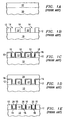
- FIG. 1A depicts a typical damascene interconnect process in which an interlevel dielectric (ILD) 12 is formed over a semiconductor body 10.
- the interlevel dielectric 12 is then patterned and etched to remove the dielectric material from the areas 14 where the interconnect lines are desired, as depicted in Fig. 1B.
- a barrier layer 16 is then deposited over the structure including over the dielectric 12 and in the areas 14 where the dielectric has been removed.
- a copper seed layer 18 is then formed over the barrier layer 16.
- the copper layer 20 is then formed from the seed layer 18 using, for example, electrochemical deposition (ECD), which is also known as an electroplating process, as depicted in Fig. 1D.
- ECD electrochemical deposition
- CMP Chemical-mechanical polishing
- the present invention provides a system for fabricating a semiconductor device.
- An interconnect structure is formed on the semiconductor device and a cap is deposited over the interconnect structure.
- the interconnect structure is annealed with the overlying cap in place.
- the cap is then removed after the interconnect structure is annealed.
- an interlevel dielectric is deposited on the cap after the interconnect structure is annealed.
- a copper interconnect structure may be formed, for example, generally according to the procedures depicted in and described with reference to Figs. 1A-1D above.
- the interlevel dielectric 102 is formed over the semiconductor body 100.
- the interlevel dielectric 102 is then patterned and etched to remove the dielectric material from the areas 118 (not shown) where interconnect lines are desired.
- the barrier layer 104 is then deposited over the structure including over the dielectric 102 and in the areas 118 (not shown) where the dielectric has been removed.
- the copper layer 106 is then formed from the seed layer 108 (not shown) using, for example, an ECD or electroplating process.
- chemical-mechanical polishing may be used to remove most of the excess copper from the copper layer 106. Chemical-mechanical polishing stops at the barrier layer 104 and may leave a thin layer of copper in seed layer 108 over the dielectric 102 and copper interconnect 110.
- Fig. 2C depicts a low temperature deposition process that forms a cap 112 over the barrier layer 104 and any remaining seed layer 108.
- the cap 112 maintains compressive forces on the copper interconnect 110 during subsequent annealing or elevated temperature processes.
- the process that forms the cap 112 may occur at temperatures that are less than 200°C.
- the cap 112 may be formed from silicon nitride, silicon oxide, silicon dioxide or organic silicon glass (OSG), for example, by conventional chemical vapor deposition (CVD) or spin-on tools, and may be easily implemented in manufacturing processes. Thickness of the cap 112 may be in the range of about 10 nm to about 200 nm, although the stress reduction in the copper interconnect 110 is relatively independent of the thickness of the cap 112, as will be described with reference to Fig. 3.
- an annealing process is performed to stabilize the copper interconnect 110.
- the annealing process may be performed at or near the interlevel dielectric deposition temperature. Compressive forces from the initial chemical-mechanical polishing and the cap 112 suppress the effects of residual tensile stress, which result from the annealing process, in the copper interconnect 110. As a result, the copper interconnect 110 is less likely to detach from the dielectric 102, thereby creating open failures, during the annealing process and subsequent high temperature processes. Production yield consequently increases because open failures are reduced.
- the cap 112 and the barrier layer 108 may be removed in a single chemical-mechanical polishing process. Deposition of the cap 112, therefore, adds minimal fabrication steps that may be easily implemented into many semiconductor manufacturing processes.
- the internal stress reduction benefit of cap 112 is relatively independent of the thickness of cap 112.
- the hydrostatic stress in the copper interconnect 110 remains between about 300 Mpa and 325 Mpa if the thickness of cap 112 is between about 50 nm and 200 nm.
- stress in an uncapped copper layer 106 after annealing is approximately 425 Mpa. Therefore, less material may be used to form the cap 112 while still gaining the stress reducing benefits of the cap 112. Process costs and time are consequently saved.
- a copper interconnect structure may be formed, for example, generally according to the procedures depicted in and described with reference to Figs. 1A-1D above.
- the interlevel dielectric 102 is formed over the semiconductor body 100.
- the interlevel dielectric 102 is then patterned and etched to remove the dielectric material from the areas 118 (not shown) where interconnect lines are desired.
- the barrier layer 104 is then deposited over the structure including over the dielectric 102 and in the areas 118 (not shown) where the dielectric has been removed.
- the copper layer 106 is then formed from the seed layer 108 (not shown) using, for example, an electrochemical deposition/electroplating process.
- chemical-mechanical polishing may be used to remove the excess copper from the copper layer 106 and also remove the barrier layer 104.
- Fig. 4C depicts a low temperature deposition process that forms a cap 114 over the copper interconnect 110 and the dielectric 102.
- the cap 112 maintains compressive forces on the copper interconnect 110 during subsequent annealing or elevated temperature processes.
- the cap 114 may also serve as an etch stop.
- the process that forms the cap 114 may occur at temperatures that are less than 200°C.
- the cap 114 may be formed from silicon nitride, silicon oxide, silicon dioxide or OSG, for example, by conventional chemical vapor deposition (CVD) or spin-on tools, and may be easily implemented in manufacturing processes. Thickness of the cap 114 may be in the range of about 10 nm to about 200 nm, although the stress reduction in the copper interconnect 110 is relatively independent of the thickness of the cap 114, as described with reference to Fig. 3.
- an annealing process is performed to stabilize the copper interconnect 110.
- the annealing process may be performed at or near the interlevel dielectric deposition temperature. Compressive forces from the initial chemical-mechanical polishing and the cap 114 suppress the effects of residual tensile stress, which result from the annealing process, in the copper interconnect 110. As a result, the copper interconnect 110 is less likely to detach from the dielectric 102, thereby creating open failures, during the annealing process and subsequent high temperature processes. Production yield consequently increases because open failures are reduced.
- the cap 114 is used as an etch stop layer and an interlevel dielectric 116 may be deposited on top of the cap 114. In this particular embodiment, deposition of the cap 114 saves the time and cost of an additional chemical-mechanical polishing by acting as an etch stop.
Landscapes
- Internal Circuitry In Semiconductor Integrated Circuit Devices (AREA)
Abstract
Description
- The invention is related generally to the field of fabricating interconnect structures for integrated circuits and, more specifically, to improving the thermal stability of copper damascene interconnect structures.
- Since the invention of integrated circuits, the number of devices on a chip has grown at a near-exponential rate. The fabrication methods of the semiconductor industry have been modified and improved continuously for almost four decades. With each improved method, the capacity of a single semiconductor chip has increased from several thousand devices to hundreds of million devices. Future improvements will require integrated circuit devices such as transistors, capacitors, and connections between devices to become even smaller and more densely populated on the chip.
- The increased packing density of the integrated circuit generates numerous challenges to the semiconductor manufacturing process. Every device must be smaller without damaging the operating characteristics of the integrated circuit devices. High packing density, low heat generation, and low power consumption, with good reliability and long operation life must be maintained without any functional device degradation. Increased packing density of integrated circuits is usually accompanied by smaller feature size.
- As integrated circuits become denser, the widths of interconnect layers that connect transistors and other semiconductor devices of the integrated circuit are reduced. As the widths of interconnect layers and semiconductor devices decrease, their resistance increases. As a result, semiconductor manufacturers seek to create smaller and faster devices by using, for example, a copper interconnect instead of a traditional aluminum interconnect. Unfortunately, copper is very difficult to etch in a semiconductor process flow. Therefore, damascene processes have been proposed to form copper interconnects.
- The damascene method involves forming a trench and/or an opening in a dielectric layer that lies beneath and on either side of the copper-containing structures. Once the trenches and/or openings are formed, a blanket layer of the copper-containing material is formed over the entire device. Electrochemical deposition (ECD) is typically the only practical method to form a blanket layer of copper. The thickness of such a layer must be at least as thick as the deepest trench and/or opening. After the trenches and/or the openings are filled with the copper-containing material, the copper-containing material over the trenches/openings is removed, e.g., by chemical-mechanical polishing (CMP), so as to leave the copper-containing material in the trenches and openings but not over the dielectric or over the uppermost portion of the trench/opening.
- Copper deposited by ECD, however, has fine grains and will re-crystallize during subsequent processing steps. During anneal steps, deposited copper interconnects frequently form voids at via bottoms and other interfaces, which may ultimately cause device failure. One solution is to anneal the copper at low (below 200°C) temperatures. A low temperature anneal, however, will not completely stabilize the deposited copper and also result in device failure. Finally, the copper may be annealed at high temperatures. Stresses within the copper interconnect structure may cause the interconnect to fail during the high temperature annealing process, which also causes via open failures.
- Copper via and interconnect fabrication processes are growing in use. One example of a conventional interconnect fabrication process is depicted in Figs. 1A-1E. In particular, Fig. 1A depicts a typical damascene interconnect process in which an interlevel dielectric (ILD) 12 is formed over a
semiconductor body 10. The interlevel dielectric 12 is then patterned and etched to remove the dielectric material from theareas 14 where the interconnect lines are desired, as depicted in Fig. 1B. Referring now to Fig. 1C, abarrier layer 16 is then deposited over the structure including over the dielectric 12 and in theareas 14 where the dielectric has been removed. Acopper seed layer 18 is then formed over thebarrier layer 16. Thecopper layer 20 is then formed from theseed layer 18 using, for example, electrochemical deposition (ECD), which is also known as an electroplating process, as depicted in Fig. 1D. Chemical-mechanical polishing (CMP) is then used to remove the excess copper and planarize thecopper 20 with the top of the interleveldielectric layer 12, as depicted in Fig. 1E. - As should now be apparent, a method of forming copper interconnect structures that does not add excessive costs or procedures to the fabrication process is now needed, providing for fabrication of more reliable semiconductor devices while overcoming the aforementioned limitations of conventional methods.
- According to a first aspect, the present invention provides a system for fabricating a semiconductor device. An interconnect structure is formed on the semiconductor device and a cap is deposited over the interconnect structure. The interconnect structure is annealed with the overlying cap in place. The cap is then removed after the interconnect structure is annealed.
- In a second aspect of the invention, an interlevel dielectric is deposited on the cap after the interconnect structure is annealed.
- For a more complete understanding of the present invention, including its features and advantages, reference is made to the following detailed description, taken in conjunction with the accompanying drawings. Corresponding numerals and symbols in the different figures refer to corresponding parts unless otherwise indicated.
- Figures 1A-1E depict a damascene interconnect fabrication process in accordance with the prior art;
- Figures 2A-2D depict an embodiment of an interconnect fabrication process in accordance with the present invention;
- Figure 3 depicts a chart of stress reduction results in accordance with the present invention; and
- Figures 4A-4D depict another embodiment of an interconnect fabrication process in accordance with the present invention.
-
- It should be understood that the principles and applications disclosed herein may be applied to a wide range of semiconductor device fabrication processes. For purposes of explanation and illustration, the present invention is hereafter described in reference to several specific embodiments of methods of semiconductor device fabrication. The present invention, however, is equally applicable in any number of fabrication processes that might benefit from the present invention.
- Turning now to the present invention as depicted in Figs. 2A-2D, a copper interconnect structure may be formed, for example, generally according to the procedures depicted in and described with reference to Figs. 1A-1D above. As depicted in Fig. 2A, the interlevel dielectric 102 is formed over the
semiconductor body 100. The interlevel dielectric 102 is then patterned and etched to remove the dielectric material from the areas 118 (not shown) where interconnect lines are desired. Thebarrier layer 104 is then deposited over the structure including over the dielectric 102 and in the areas 118 (not shown) where the dielectric has been removed. Thecopper layer 106 is then formed from the seed layer 108 (not shown) using, for example, an ECD or electroplating process. - Turning now to Fig. 2B, chemical-mechanical polishing may be used to remove most of the excess copper from the
copper layer 106. Chemical-mechanical polishing stops at thebarrier layer 104 and may leave a thin layer of copper inseed layer 108 over the dielectric 102 andcopper interconnect 110. - Fig. 2C depicts a low temperature deposition process that forms a
cap 112 over thebarrier layer 104 and any remainingseed layer 108. Thecap 112 maintains compressive forces on thecopper interconnect 110 during subsequent annealing or elevated temperature processes. The process that forms thecap 112 may occur at temperatures that are less than 200°C. Thecap 112 may be formed from silicon nitride, silicon oxide, silicon dioxide or organic silicon glass (OSG), for example, by conventional chemical vapor deposition (CVD) or spin-on tools, and may be easily implemented in manufacturing processes. Thickness of thecap 112 may be in the range of about 10 nm to about 200 nm, although the stress reduction in thecopper interconnect 110 is relatively independent of the thickness of thecap 112, as will be described with reference to Fig. 3. - In Fig. 2D, an annealing process is performed to stabilize the
copper interconnect 110. The annealing process may be performed at or near the interlevel dielectric deposition temperature. Compressive forces from the initial chemical-mechanical polishing and thecap 112 suppress the effects of residual tensile stress, which result from the annealing process, in thecopper interconnect 110. As a result, thecopper interconnect 110 is less likely to detach from the dielectric 102, thereby creating open failures, during the annealing process and subsequent high temperature processes. Production yield consequently increases because open failures are reduced. After the annealing process, thecap 112 and thebarrier layer 108 may be removed in a single chemical-mechanical polishing process. Deposition of thecap 112, therefore, adds minimal fabrication steps that may be easily implemented into many semiconductor manufacturing processes. - As depicted in Fig. 3, the internal stress reduction benefit of
cap 112 is relatively independent of the thickness ofcap 112. For example, after annealing, the hydrostatic stress in thecopper interconnect 110 remains between about 300 Mpa and 325 Mpa if the thickness ofcap 112 is between about 50 nm and 200 nm. For comparison, stress in anuncapped copper layer 106 after annealing is approximately 425 Mpa. Therefore, less material may be used to form thecap 112 while still gaining the stress reducing benefits of thecap 112. Process costs and time are consequently saved. - Another embodiment of the present invention is depicted in Figs. 4A-4D. A copper interconnect structure may be formed, for example, generally according to the procedures depicted in and described with reference to Figs. 1A-1D above. As depicted in Fig. 4A, the
interlevel dielectric 102 is formed over thesemiconductor body 100. Theinterlevel dielectric 102 is then patterned and etched to remove the dielectric material from the areas 118 (not shown) where interconnect lines are desired. Thebarrier layer 104 is then deposited over the structure including over the dielectric 102 and in the areas 118 (not shown) where the dielectric has been removed. Thecopper layer 106 is then formed from the seed layer 108 (not shown) using, for example, an electrochemical deposition/electroplating process. - As depicted in Fig. 4B, chemical-mechanical polishing may be used to remove the excess copper from the
copper layer 106 and also remove thebarrier layer 104. - Fig. 4C depicts a low temperature deposition process that forms a
cap 114 over thecopper interconnect 110 and the dielectric 102. Thecap 112 maintains compressive forces on thecopper interconnect 110 during subsequent annealing or elevated temperature processes. In this particular embodiment, thecap 114 may also serve as an etch stop. The process that forms thecap 114 may occur at temperatures that are less than 200°C. Thecap 114 may be formed from silicon nitride, silicon oxide, silicon dioxide or OSG, for example, by conventional chemical vapor deposition (CVD) or spin-on tools, and may be easily implemented in manufacturing processes. Thickness of thecap 114 may be in the range of about 10 nm to about 200 nm, although the stress reduction in thecopper interconnect 110 is relatively independent of the thickness of thecap 114, as described with reference to Fig. 3. - In Fig. 4D, an annealing process is performed to stabilize the
copper interconnect 110. The annealing process may be performed at or near the interlevel dielectric deposition temperature. Compressive forces from the initial chemical-mechanical polishing and thecap 114 suppress the effects of residual tensile stress, which result from the annealing process, in thecopper interconnect 110. As a result, thecopper interconnect 110 is less likely to detach from the dielectric 102, thereby creating open failures, during the annealing process and subsequent high temperature processes. Production yield consequently increases because open failures are reduced. After the annealing process, thecap 114 is used as an etch stop layer and aninterlevel dielectric 116 may be deposited on top of thecap 114. In this particular embodiment, deposition of thecap 114 saves the time and cost of an additional chemical-mechanical polishing by acting as an etch stop. - Although this invention has been described with reference to illustrative embodiments, this description is not intended to be construed in a limiting sense. Upon reference to the description, it will be apparent to persons skilled in the art that various modifications and combinations of the illustrative embodiments as well as other embodiments of the invention can be made without departing from the scope of the invention. It is therefore intended that the appended claims encompass any such modifications or embodiments.
Claims (10)
- A method of fabricating a semiconductor device, comprising the steps of:forming an interconnect structure;depositing a cap over the interconnect structure;annealing the interconnect structure; andremoving the cap.
- The method of claim 1, wherein the interconnect structure is formed from copper.
- The method of claim 1 or 2, wherein the interconnect structure is formed by electrochemical deposition.
- The method of any one of claims 1 to 3, wherein the cap is deposited at a temperature about or less than 200°C.
- The method of any one of claims 1 to 4, wherein the cap is deposited by chemical vapor deposition.
- The method of any one of claims 1 to 4, wherein the cap is deposited by a spin-on tool.
- The method of any one of claims 1 to 6, wherein the step of annealing the interconnect structure is annealing at a temperature above 200°C.
- The method of any one of claims 1 to 6, wherein the step of annealing the interconnect structure is annealing at 780°C.
- The method of any one of claims 1 to 8, wherein the step of removing the cap is by chemical-mechanical polishing.
- The method of any one of claims 1 to 9, wherein the step of depositing the cap comprises depositing a cap from a material chosen from the group of silicon nitride, silicon oxide, silicon dioxide or organic silicon glass.
Applications Claiming Priority (4)
| Application Number | Priority Date | Filing Date | Title |
|---|---|---|---|
| US114778 | 1987-10-30 | ||
| US344465 | 1999-06-25 | ||
| US34446501P | 2001-12-28 | 2001-12-28 | |
| US10/114,778 US6903000B2 (en) | 2001-12-28 | 2002-04-03 | System for improving thermal stability of copper damascene structure |
Publications (2)
| Publication Number | Publication Date |
|---|---|
| EP1326274A2 true EP1326274A2 (en) | 2003-07-09 |
| EP1326274A3 EP1326274A3 (en) | 2009-03-04 |
Family
ID=26812531
Family Applications (1)
| Application Number | Title | Priority Date | Filing Date |
|---|---|---|---|
| EP02102840A Ceased EP1326274A3 (en) | 2001-12-28 | 2002-12-19 | System for improving thermal stability of copper damascene structure |
Country Status (2)
| Country | Link |
|---|---|
| US (2) | US6903000B2 (en) |
| EP (1) | EP1326274A3 (en) |
Families Citing this family (6)
| Publication number | Priority date | Publication date | Assignee | Title |
|---|---|---|---|---|
| TW578137B (en) * | 2002-10-24 | 2004-03-01 | Chi Mei Optoelectronics Corp | Driving circuit of a liquid crystal display device |
| KR20060073189A (en) * | 2004-12-24 | 2006-06-28 | 동부일렉트로닉스 주식회사 | Copper wiring formation method of semiconductor device |
| US7972954B2 (en) * | 2006-01-24 | 2011-07-05 | Infineon Technologies Ag | Porous silicon dielectric |
| DE102007035837A1 (en) * | 2007-07-31 | 2009-02-05 | Advanced Micro Devices, Inc., Sunnyvale | Semiconductor device with a grain orientation layer |
| US20150206798A1 (en) * | 2014-01-17 | 2015-07-23 | Taiwan Semiconductor Manufacturing Company, Ltd. | Interconnect Structure And Method of Forming |
| US20250338521A1 (en) * | 2024-04-29 | 2025-10-30 | Texas Instruments Incorporated | Thin film resistor integration with terminals |
Family Cites Families (14)
| Publication number | Priority date | Publication date | Assignee | Title |
|---|---|---|---|---|
| EP0526889B1 (en) * | 1991-08-06 | 1997-05-07 | Nec Corporation | Method of depositing a metal or passivation fabric with high adhesion on an insulated semiconductor substrate |
| JPH05243226A (en) * | 1992-03-03 | 1993-09-21 | Nec Corp | Manufacture of semiconductor device |
| US5561082A (en) * | 1992-07-31 | 1996-10-01 | Kabushiki Kaisha Toshiba | Method for forming an electrode and/or wiring layer by reducing copper oxide or silver oxide |
| US5668055A (en) * | 1995-05-05 | 1997-09-16 | Applied Materials, Inc. | Method of filling of contact openings and vias by self-extrusion of overlying compressively stressed matal layer |
| US5814557A (en) * | 1996-05-20 | 1998-09-29 | Motorola, Inc. | Method of forming an interconnect structure |
| JPH1032203A (en) * | 1996-07-17 | 1998-02-03 | Toshiba Corp | Method for manufacturing semiconductor device |
| US5956612A (en) * | 1996-08-09 | 1999-09-21 | Micron Technology, Inc. | Trench/hole fill processes for semiconductor fabrication |
| US5926736A (en) * | 1996-10-30 | 1999-07-20 | Stmicroelectronics, Inc. | Low temperature aluminum reflow for multilevel metallization |
| JPH10199881A (en) * | 1997-01-13 | 1998-07-31 | Nec Corp | Method for manufacturing semiconductor device |
| US7510961B2 (en) * | 1997-02-14 | 2009-03-31 | Micron Technology, Inc. | Utilization of energy absorbing layer to improve metal flow and fill in a novel interconnect structure |
| US6100184A (en) * | 1997-08-20 | 2000-08-08 | Sematech, Inc. | Method of making a dual damascene interconnect structure using low dielectric constant material for an inter-level dielectric layer |
| US6274499B1 (en) * | 1999-11-19 | 2001-08-14 | Chartered Semiconductor Manufacturing Ltd. | Method to avoid copper contamination during copper etching and CMP |
| US6602653B1 (en) * | 2000-08-25 | 2003-08-05 | Micron Technology, Inc. | Conductive material patterning methods |
| US6426293B1 (en) * | 2001-06-01 | 2002-07-30 | Advanced Micro Devices, Inc. | Minimizing resistance and electromigration of interconnect by adjusting anneal temperature and amount of seed layer dopant |
-
2002
- 2002-04-03 US US10/114,778 patent/US6903000B2/en not_active Expired - Lifetime
- 2002-12-19 EP EP02102840A patent/EP1326274A3/en not_active Ceased
-
2005
- 2005-03-24 US US11/090,103 patent/US20050186788A1/en not_active Abandoned
Non-Patent Citations (1)
| Title |
|---|
| None * |
Also Published As
| Publication number | Publication date |
|---|---|
| US20050186788A1 (en) | 2005-08-25 |
| US6903000B2 (en) | 2005-06-07 |
| US20030124828A1 (en) | 2003-07-03 |
| EP1326274A3 (en) | 2009-03-04 |
Similar Documents
| Publication | Publication Date | Title |
|---|---|---|
| KR100564188B1 (en) | Semiconductor integrated circuit device and its manufacturing method | |
| US7332428B2 (en) | Metal interconnect structure and method | |
| US6071809A (en) | Methods for forming high-performing dual-damascene interconnect structures | |
| JP3973467B2 (en) | Manufacturing method of semiconductor device | |
| US6900539B2 (en) | Semiconductor device and method for manufacturing the same | |
| US6417094B1 (en) | Dual-damascene interconnect structures and methods of fabricating same | |
| EP1672688A1 (en) | Formation of deep via airgaps for three dimensional wafer to wafer interconnect | |
| US12243839B2 (en) | Bonded semiconductor structure utilizing concave/convex profile design for bonding pads | |
| US6674168B1 (en) | Single and multilevel rework | |
| EP3279931A1 (en) | Method for fabricating cu interconnection using graphene | |
| US6191031B1 (en) | Process for producing multi-layer wiring structure | |
| US6903000B2 (en) | System for improving thermal stability of copper damascene structure | |
| JPH10284600A (en) | Semiconductor device and manufacturing method thereof | |
| US20020127849A1 (en) | Method of manufacturing dual damascene structure | |
| US7897508B2 (en) | Method to eliminate Cu dislocation for reliability and yield | |
| KR100705950B1 (en) | Metal wiring formation method of semiconductor device | |
| US7572717B2 (en) | Method of manufacturing semiconductor device | |
| US6541368B2 (en) | Metal lines of semiconductor devices and methods for forming | |
| JP2002198424A (en) | Semiconductor device and manufacturing method thereof | |
| CN119786476A (en) | A low temperature hybrid bonding interconnect structure and manufacturing method | |
| JP2005183888A (en) | Semiconductor device and manufacturing method of semiconductor device | |
| JPH118244A (en) | Method for manufacturing semiconductor device | |
| JP2001168187A (en) | Method for manufacturing semiconductor device | |
| US20080194096A1 (en) | Method of manufacturing semiconductor device | |
| JP2000228445A (en) | Semiconductor device and manufacturing method thereof |
Legal Events
| Date | Code | Title | Description |
|---|---|---|---|
| PUAI | Public reference made under article 153(3) epc to a published international application that has entered the european phase |
Free format text: ORIGINAL CODE: 0009012 |
|
| AK | Designated contracting states |
Designated state(s): AT BE BG CH CY CZ DE DK EE ES FI FR GB GR IE IT LI LU MC NL PT SE SI SK TR |
|
| AX | Request for extension of the european patent |
Extension state: AL LT LV MK RO |
|
| PUAL | Search report despatched |
Free format text: ORIGINAL CODE: 0009013 |
|
| AK | Designated contracting states |
Kind code of ref document: A3 Designated state(s): AT BE BG CH CY CZ DE DK EE ES FI FR GB GR IE IT LI LU MC NL PT SE SI SK TR |
|
| AX | Request for extension of the european patent |
Extension state: AL LT LV MK RO |
|
| 17P | Request for examination filed |
Effective date: 20090904 |
|
| AKX | Designation fees paid |
Designated state(s): DE FR GB |
|
| 17Q | First examination report despatched |
Effective date: 20130814 |
|
| STAA | Information on the status of an ep patent application or granted ep patent |
Free format text: STATUS: THE APPLICATION HAS BEEN REFUSED |
|
| 18R | Application refused |
Effective date: 20190217 |