EP1326203A2 - Verfahren und Anordnung zum Schutz von digitalen Schaltungsteilen - Google Patents
Verfahren und Anordnung zum Schutz von digitalen Schaltungsteilen Download PDFInfo
- Publication number
- EP1326203A2 EP1326203A2 EP02102850A EP02102850A EP1326203A2 EP 1326203 A2 EP1326203 A2 EP 1326203A2 EP 02102850 A EP02102850 A EP 02102850A EP 02102850 A EP02102850 A EP 02102850A EP 1326203 A2 EP1326203 A2 EP 1326203A2
- Authority
- EP
- European Patent Office
- Prior art keywords
- gate
- inverter
- digital circuit
- arrangement according
- circuit parts
- Prior art date
- Legal status (The legal status is an assumption and is not a legal conclusion. Google has not performed a legal analysis and makes no representation as to the accuracy of the status listed.)
- Withdrawn
Links
Images
Classifications
-
- H10W42/40—
-
- G—PHYSICS
- G06—COMPUTING OR CALCULATING; COUNTING
- G06K—GRAPHICAL DATA READING; PRESENTATION OF DATA; RECORD CARRIERS; HANDLING RECORD CARRIERS
- G06K19/00—Record carriers for use with machines and with at least a part designed to carry digital markings
- G06K19/06—Record carriers for use with machines and with at least a part designed to carry digital markings characterised by the kind of the digital marking, e.g. shape, nature, code
- G06K19/067—Record carriers with conductive marks, printed circuits or semiconductor circuit elements, e.g. credit or identity cards also with resonating or responding marks without active components
- G06K19/07—Record carriers with conductive marks, printed circuits or semiconductor circuit elements, e.g. credit or identity cards also with resonating or responding marks without active components with integrated circuit chips
- G06K19/073—Special arrangements for circuits, e.g. for protecting identification code in memory
- G06K19/07309—Means for preventing undesired reading or writing from or onto record carriers
- G06K19/07372—Means for preventing undesired reading or writing from or onto record carriers by detecting tampering with the circuit
Definitions
- the invention relates to a method and an arrangement for protecting digital circuit parts, which can be used in particular to store storage units on such digital circuits, in particular smart card controllers, which contain secret data, protect against attacks that follow the approach, digital circuit parts, in particular the digital part of a smart card controller, due to brief voltage drops, e.g. by flashes of light to put them in an undefined state.
- smart cards In a smart card are data storage and arithmetic logic Units integrated in a single chip a few square millimeters in size. Smart cards are used in particular as telephone cards, GSM SIM cards, in the banking sector and used in healthcare. The smart card is thus ubiquitous Computing platform.
- Smart cards are currently primarily used as a safe place to keep secret data and viewed as a secure execution platform for cryptographic algorithms.
- the Assumption of a relatively high security of the data and algorithms on the card lies in the Hardware structure of the card and the external interfaces are justified.
- Critical data such as secret key a public key procedure
- access from outside can even be completely removed.
- a smart card is able to execute algorithms without the Execution of the individual operations can be observed from the outside.
- the algorithms themselves can be protected against changes and readouts on the card.
- object-oriented The smart card can be understood as an abstract data type, the over has a well-defined interface, a specified behavior and even in is able to comply with certain integrity conditions regarding its condition sure.
- Smart cards There are two main types of smart cards. Own memory cards only a serial interface, addressing and security logic and ROM and EEPROM memory. These cards have limited functionality and serve a specific application. But they are particularly cheap to manufacture. As Smart cards made from microprocessor cards are in principle a complete universal computer represents.
- each phase is carried out by a company that specializes in the respective work carried out.
- the semiconductors When manufacturing the semiconductors is especially hard-wired for cards Security logic to pay attention to good internal security. So from the manufacturer a complete final test can be carried out, the complete memory must be free be accessible. The chip is only secured by a transport code after the final test. After that, access to the card memory is only for authorized entities that have the Knowing the transport code, possible. Theft of brand new semiconductors is therefore not an option Consequences.
- Authorized bodies can be personalizers or card issuers. For embedding and printing no further security functions are necessary. The concerned Companies do not need to know the transport code.
- the issuing body e.g. Bank, telephone company, health insurance etc.
- the personal data in the card This process is called personalization. For them, the knowledge of the transport code necessary.
- Chips on chip cards apply to the encryption of this data; a fuse against unauthorized access to the chip is minimal or non-existent; at a Chip card is usually a mechanical access to the data or its extraction chemical removal of the plastic layer with an existing passivation cover of the pierced stylus possible.
- Some hacker attacks also pursue the approach of converting the digital part of a smart card controller into an undefined one Bring condition. Brief voltage drops, e.g. by Flash attacks provoked.
- WO 98/18102 describes a method and an arrangement for protecting electronic ones Computing units described against unwanted access.
- the computing unit is at one or more measuring points the casing determines measured values after at a specified signal feed point signals defined by the computing unit have been applied to the casing.
- a signature is formed from the measured values recorded and in a register stored. Because any injury or damage the special properties of the sheath change, the measured value recorded after an injury results in another Signature as filed in the register for the intact casing. A comparison of the In this case, signatures lead to an error message and further messages for one Case provided steps.
- US 5,465,349 describes a security method for monitoring integrated Circuits to undefined states; first of all, before each data transfer to an external device and secondly before any change (write or delete) from Memory data of the integrated circuit, which is usually in an EPROM or EEPROM are stored, a status query of one or more security registers.
- the Status of the security register is changed if the system has an undefined state detects, for this purpose also sensors, e.g. a sensor which measures the working frequency of the circuit monitored, or an optical sensor can be used can.
- US Pat. No. 6,092,147 describes a distributed check of hardware-independent, executable bytecode described by a computer to a virtual machine is transferred to run there.
- the test is carried out as follows. After the test on the sending computer system has been completed, the test result first confirmed by the virtual machine before the bytecode on the virtual machine is performed.
- protection against unauthorized access to protected memory of an electronic system, in particular of a computer system improved by performing the following steps: setting the Computer system in a mode in which a confirmation process is performed; then a safety circuit is switched into a first one before leaving this operating mode set status; the status of the safety circuit is then checked, the operations performed by the computer system be stopped if the safety circuit is in a different one than that given status.
- the invention is therefore based on the object of a method and an arrangement of the Specify generic type, through which the disadvantages of conventional protective measures be fixed and in particular it is prevented that secret, in one digital circuit part stored data become accessible after it has been possible to bring this digital circuit part into an undefined state.
- An arrangement for protecting digital circuit parts is advantageously constructed in such a way that that the digital circuit part (glue logic) comprises at least one digital sensor 1.
- Another advantage of the method according to the invention is that the voltage drops can be detected within the glue logic.
- this is the invention Process can be used to reduce voltage dips within a smart card controller to detect.
- the Sensors are activated by setting the reset signal to logic zero.
- the senor (s) is (are) designed as a special standard cell, which a NOR gate, an inverter and a capacitor.
- the NOR gate and inverter are connected as a latch.
- the standard cell (s) has a NOR gate and an inverter, the input of the NOR gate with the output of the inverter and a capacitor with the Supply voltage is connected and the input of the inverter to the output of the NOR gate is connected and the reset signal can be applied to the input of the NOR gate and the error signal can be tapped at the output of the NOR gate.
- the threshold voltage in the NOR gate and the transistors used in the inverter are designed differently.
- the sensor (s) is designed as a light or voltage sensor is (are).
- the so-called glue logic is part of a smart card controller.
- a special sensor system distributed over the digital part (glue logic), protects against the above Attacks. Because the sensors are located within the glue logic, the following advantage is obtained. First, the sensors can experience voltage dips there recognize where they are most critical. Second, the sensors are no more than that recognizable.
- the security of the entire chip is significantly increased. Attacks on the glue logic itself, e.g. due to flashes of light, are recognized directly on site.
- the sensors are further very small, which means that a higher number of instances is distributed on the glue logic can be made without losing a lot of chip area.
- the sensors are not recognizable as such or to be distinguished from the standard cells.
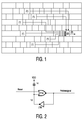
- the digital part according to FIG. 1 is presented below.
- the output signals of standard cells 1 operating as sensors are linked to one another with an OR circuit 2.
- a final output signal 3 of the OR circuit 2 is active when one or more sensors 1 deliver an error signal.
- the exemplary arrangement shown in FIG. 2 of a sensor 1 constructed as a standard cell comprises a NOR gate 1a and an inverter 1b; these work as a latch.
- a node 1d, in which an input of the NOR gate 1a is connected to the output of the inverter 1b, is connected to a supply voltage VDD via a capacitor 1c.
- the input of the inverter 1b is connected to the output of the NOR gate 1a.
- a reset signal can be applied to a further input of NOR gate 1a and the error signal to be supplied by this sensor 1 can be tapped at the output of NOR gate 1a.
- the latch comprising the NOR gate 1a and the inverter 1b can by means of the reset signal be reset so that the error signal emitted by sensor 1 becomes inactive and assumes the state logic "0". In this state, node 1d is logically "1".
Landscapes
- Engineering & Computer Science (AREA)
- Computer Hardware Design (AREA)
- Computer Security & Cryptography (AREA)
- General Engineering & Computer Science (AREA)
- Microelectronics & Electronic Packaging (AREA)
- Physics & Mathematics (AREA)
- General Physics & Mathematics (AREA)
- Theoretical Computer Science (AREA)
- Storage Device Security (AREA)
- Techniques For Improving Reliability Of Storages (AREA)
Abstract
Description
- Herstellen des Halbleiters,
- Einbetten des Halbleiters,
- Bedrucken der Karte,
- Personalisierung der Karte,
- Ausgeben der Karte.
- Störungsempfindlichkeit ― Eng benachbarte digitale Schaltungsteile stören die empfindliche Sensorik.
- Schaltungselemente ― In analogen Schaltungen werden nicht nur die NMOS- und PMOS-Standardtransistoren verwendet, sondern auch speziell dimensionierte Transistoren, Kondensatoren und Widerstände. Diese passen aufgrund ihrer Größe nicht in das vorgegebene Raster der Standardzellen.
- Fig. 1
- eine Verteilung der speziellen Standardzellen als Sensoren in einem Digitalteil,
- Fig. 2
- einen Aufbau eines als Standardzelle aufgebauten Sensors.
Die in Fig. 2 gezeigte, beispielhafte Anordnung eines als Standardzelle aufgebauten Sensors 1 umfaßt ein NOR-Gatter 1a und einen Inverter 1b; diese arbeiten als Latch. Ein Knoten 1d, in dem ein Eingang des NOR-Gatters 1a mit dem Ausgang des Inverters 1b verbunden ist, ist über einen Kondensator 1c mit einer Versorgungsspannung VDD verbunden. Der Eingang des Inverters 1b ist mit dem Ausgang des NOR-Gatters 1a verbunden. An einem weiteren Eingang des NOR-Gatters 1a ist ein Reset-Signal anlegbar und am Ausgang des NOR-Gatters 1a ist das von diesem Sensor 1 zu liefernde Fehlersignal abgreifbar.
- 1
- als Sensor arbeitende Standardzelle
- 1a
- NOR-Gatter
- 1b
- Inverter
- 1c
- Kondensator
- 1d
- Knoten
- 2
- ODER-Schaltung
- 3
- Ausgangssignal
Claims (13)
- Verfahren zum Schutz von digitalen Schaltungsteilen,
dadurch gekennzeichnet, dass Spannungseinbrüche detektiert werden. - Verfahren nach Anspruch 1,
dadurch gekennzeichnet, dass die Spannungseinbrüche innerhalb wenigstens eines der (als "Glue-Logic" bezeichneten) digitalen Schaltungsteile detektiert werden. - Verfahren nach einem der vorhergehenden Ansprüche,
dadurch gekennzeichnet, dass die Spannungseinbrüche innerhalb eines Smartcard-Controllers detektiert werden. - Verfahren nach einem der vorhergehenden Ansprüche,
dadurch gekennzeichnet, dass die Spannungseinbrüche durch digitale Sensoren detektiert werden. - Verfahren nach einem der vorhergehenden Ansprüche,
dadurch gekennzeichnet, dass die Sensoren aktiviert werden, indem das Reset-Signal auf logisch Null gesetzt wird. - Anordnung zum Schutz von digitalen Schaltungsteilen
dadurch gekennzeichnet, dass der digitale Schaltungsteil (Glue-Logic) mindestens einen digitalen Sensor (1) umfaßt. - Anordnung nach Anspruch 6,
dadurch gekennzeichnet, dass beim Vorhandensein mehrerer Sensoren (1) diese mit einer ODER-Schaltung (2) verknüpft sind. - Anordnung nach einem der Ansprüche 6 oder 7,
dadurch gekennzeichnet, dass der (die) Sensor(en) (1) als spezielle Standardzelle ausgebildet ist (sind), welche ein NOR-Gatter (1a), einen Inverter (1b) und einen Kondensator (1c) umfaßt. - Anordnung nach Anspruch 8,
dadurch gekennzeichnet, dass NOR-Gatter (1a) und Inverter (1b) als Latch geschaltet sind. - Anordnung nach Anspruch 8,
dadurch gekennzeichnet, dass die Standardzelle(n) (1) ein NOR-Gatter (1a) sowie einen Inverter (1b) aufweist (aufweisen), wobei ein Eingang des NOR-Gatters (1a) mit dem Ausgang des Inverters (1b) sowie über einen Kondensator (1c) mit einer Versorgungsspannung (VDD) verbunden ist und der Eingang des Inverters (1b) mit dem Ausgang des NOR-Gatters (1a) verbunden ist und an einem weiteren Eingang des NOR-Gatters (1a) das Reset-Signal anlegbar und am Ausgang des NOR-Gatters (1a) ein Fehlersignal abgreifbar ist. - Anordnung nach einem der Ansprüche 8 bis 10,
dadurch gekennzeichnet, dass Schwellenspannungen im NOR-Gatter (1a) und im Inverter (1b) verwendeter Transistoren unterschiedlich ausgelegt sind. - Anordnung nach einem der Ansprüche 6 bis 11,
dadurch gekennzeichnet, dass der (die) Sensor(en) (1) als Licht- oder Spannungssensor ausgebildet ist (sind). - Anordnung nach einem der Ansprüche 6 bis 12,
dadurch gekennzeichnet, dass die "Glue-Logic" Bestandteil eines Smartcard-Controllers ist.
Applications Claiming Priority (2)
| Application Number | Priority Date | Filing Date | Title |
|---|---|---|---|
| DE10164419 | 2001-12-29 | ||
| DE10164419A DE10164419A1 (de) | 2001-12-29 | 2001-12-29 | Verfahren und Anordnung zum Schutz von digitalen Schaltungsteilen |
Publications (2)
| Publication Number | Publication Date |
|---|---|
| EP1326203A2 true EP1326203A2 (de) | 2003-07-09 |
| EP1326203A3 EP1326203A3 (de) | 2003-10-01 |
Family
ID=7711111
Family Applications (1)
| Application Number | Title | Priority Date | Filing Date |
|---|---|---|---|
| EP02102850A Withdrawn EP1326203A3 (de) | 2001-12-29 | 2002-12-20 | Verfahren und Anordnung zum Schutz von digitalen Schaltungsteilen |
Country Status (5)
| Country | Link |
|---|---|
| US (1) | US20030133241A1 (de) |
| EP (1) | EP1326203A3 (de) |
| JP (1) | JP2003233790A (de) |
| CN (1) | CN1430153A (de) |
| DE (1) | DE10164419A1 (de) |
Cited By (1)
| Publication number | Priority date | Publication date | Assignee | Title |
|---|---|---|---|---|
| DE102007059923B4 (de) | 2006-12-06 | 2022-03-17 | Samsung Electronics Co., Ltd. | Smart-Card |
Families Citing this family (7)
| Publication number | Priority date | Publication date | Assignee | Title |
|---|---|---|---|---|
| KR100884566B1 (ko) * | 2006-11-16 | 2009-02-19 | 삼성전자주식회사 | 레이저 어택 검출기를 갖는 스마트 카드 |
| IL199272A0 (en) | 2009-06-10 | 2012-07-16 | Nds Ltd | Protection of secret value using hardware instability |
| EP2369622B1 (de) | 2010-03-24 | 2015-10-14 | STMicroelectronics Rousset SAS | Verfahren und Vorrichtung für Gegenmassnahme gegenüber einem Angriff durch Fehlerinjektion in einem elektronischen Mikroschaltungskarte |
| FR2958078B1 (fr) * | 2010-03-24 | 2012-04-20 | St Microelectronics Rousset | Procede et dispositif de contremesure contre une attaque par injection d'erreur dans un microcircuit electronique |
| EP2541599A1 (de) * | 2011-06-28 | 2013-01-02 | Nxp B.V. | Sicherheitshalbleiterprodukt |
| CN107544861A (zh) * | 2016-06-24 | 2018-01-05 | 国民技术股份有限公司 | 具有攻击防护结构的系统 |
| CN111460747B (zh) * | 2020-04-10 | 2023-03-31 | 重庆百瑞互联电子技术有限公司 | 一种用于集成电路设计的标准单元追踪方法 |
Family Cites Families (12)
| Publication number | Priority date | Publication date | Assignee | Title |
|---|---|---|---|---|
| FR2619959B1 (fr) * | 1987-08-31 | 1991-06-14 | Thomson Semiconducteurs | Circuit de detection de lumiere |
| FR2649817B1 (fr) * | 1989-07-13 | 1993-12-24 | Gemplus Card International | Carte a microcircuit protegee contre l'intrusion |
| FR2668274B1 (fr) * | 1990-10-19 | 1992-12-31 | Gemplus Card Int | Circuit integre a securite d'acces amelioree. |
| FR2676294B1 (fr) * | 1991-05-06 | 1993-07-16 | Gemplus Card Int | Procede de verrouillage pour carte a memoire. |
| DE19601390C2 (de) * | 1996-01-16 | 1998-07-16 | Siemens Ag | Mikrochip |
| US5835594A (en) * | 1996-02-09 | 1998-11-10 | Intel Corporation | Methods and apparatus for preventing unauthorized write access to a protected non-volatile storage |
| US5935223A (en) * | 1996-05-21 | 1999-08-10 | Texas Instruments Incorporated | System for blocking access to a computer device using a glue logic circuit operable to force a target computer device to perform a target abort |
| GB2319602B (en) * | 1996-11-21 | 2000-10-04 | Motorola Ltd | Light detection device |
| US5847587A (en) * | 1997-01-07 | 1998-12-08 | Holtek Microelectronics Inc. | Means for instantaneously detecting abnormal voltage in a micro controller |
| US6092147A (en) * | 1997-04-15 | 2000-07-18 | Sun Microsystems, Inc. | Virtual machine with securely distributed bytecode verification |
| US5999392A (en) * | 1998-06-26 | 1999-12-07 | Industrial Technology Research Institute | Reset circuit with transient detection function |
| US6658597B1 (en) * | 1999-10-22 | 2003-12-02 | Industrial Technology Research Institute | Method and apparatus for automatic recovery of microprocessors/microcontrollers during electromagnetic compatibility (EMC) testing |
-
2001
- 2001-12-29 DE DE10164419A patent/DE10164419A1/de not_active Withdrawn
-
2002
- 2002-12-20 US US10/324,767 patent/US20030133241A1/en not_active Abandoned
- 2002-12-20 EP EP02102850A patent/EP1326203A3/de not_active Withdrawn
- 2002-12-26 CN CN02128167.XA patent/CN1430153A/zh active Pending
- 2002-12-26 JP JP2002378080A patent/JP2003233790A/ja active Pending
Cited By (1)
| Publication number | Priority date | Publication date | Assignee | Title |
|---|---|---|---|---|
| DE102007059923B4 (de) | 2006-12-06 | 2022-03-17 | Samsung Electronics Co., Ltd. | Smart-Card |
Also Published As
| Publication number | Publication date |
|---|---|
| US20030133241A1 (en) | 2003-07-17 |
| EP1326203A3 (de) | 2003-10-01 |
| JP2003233790A (ja) | 2003-08-22 |
| CN1430153A (zh) | 2003-07-16 |
| DE10164419A1 (de) | 2003-07-17 |
Similar Documents
| Publication | Publication Date | Title |
|---|---|---|
| DE112007002037B4 (de) | Erkennen von auf Strahlung basierenden Angriffen | |
| DE10162306A1 (de) | Verfahren und Anordnung zur Verifikation von NV-Fuses sowie ein entsprechendes Computerprogrammprodukt und ein entsprechendes computerlesbares Speichermedium | |
| DE69527773T2 (de) | Schaltungsanordnung zur Überwachung der Benutzung von Funktionen in einem integrierten Schaltungkreis | |
| EP0891601B1 (de) | Chipkarte | |
| DE69404674T2 (de) | Speicherkarte und verfahren zum betrieb | |
| DE69327181T2 (de) | Massenspeicherkarte für einen Mikrocomputer | |
| DE69715282T2 (de) | Schutzanordnung für ein Halbleiterplättchen | |
| DE10164415A1 (de) | Verfahren und Anordnung zur Programmierung und Verifizierung von EEPROM-Pages sowie ein entsprechendes Computerprogrammprodukt und ein entsprechendes computerlesbares Speichermedium | |
| DE69913142T2 (de) | Vorrichtung und verfahren zur sicheren informationsverarbeitung | |
| EP0280035B1 (de) | Verfahren zum Sichern von Programmen und zur Integritätskontrolle gesicherter Programme | |
| EP1326203A2 (de) | Verfahren und Anordnung zum Schutz von digitalen Schaltungsteilen | |
| EP1664978B1 (de) | Vorrichtung und verfahren zur sicheren ausführung eines programmes | |
| EP1338970B1 (de) | Verfahren und Anordnung zur Zugriffssteuerung auf EEPROMs sowie ein entsprechendes Computerprogrammprodukt und ein entsprechendes computerlesbares Speichermedium | |
| DE602004011965T2 (de) | Verfahren und schaltung zum identifizieren und/oder verifizieren von hardware und/oder software eines geräts und eines mit dem gerät arbeitenden datenträgers | |
| DE102004036889A1 (de) | Detektorschaltung und Zugriffdetektionsverfahren für eine Chipkarte | |
| EP2652665B1 (de) | Portabler datenträger mit fehlbedienungszähler | |
| WO1998041880A2 (de) | Integrierte schaltung und verfahren zum testen der integrierten schaltung | |
| DE102006035610B4 (de) | Speicherzugriffssteuerung und Verfahren zur Speicherzugriffssteuerung | |
| DE10162291A1 (de) | Verfahren und Anordnung zur Verhinderung unbefugten Ausführens von Computerprogrammen sowie ein entsprechendes Computerprogrammprodukt und ein entsprechendes computerlesbares Speichermedium | |
| DE10162310A1 (de) | Verfahren und Anordnung zur Übertragung von Signalen von erzeugenden Funktionseinheiten an verarbeitende Funktionseinheiten elektrischer Schaltungen | |
| WO2004036649A1 (de) | Chip mit angriffsschutz | |
| DE10162307A1 (de) | Verfahren und Anordnung zur Herstellung von maskenprogrammierten ROMs unter Verwendung einer mehrere Systeme umfassenden Maske sowie ein entsprechendes Computerprogrammprodukt und ein entsprechendes computerlesbares Speichermedium | |
| DE10258178B4 (de) | Schaltung mit Sicherheitsmaßnahmen gegen Ausspionieren der Schaltung | |
| DE102005042790A1 (de) | Integrierte Schaltungsanordnung und Verfahren zum Betrieb einer solchen | |
| EP1899883B1 (de) | Verfahren zum schutz vertraulicher daten |
Legal Events
| Date | Code | Title | Description |
|---|---|---|---|
| PUAI | Public reference made under article 153(3) epc to a published international application that has entered the european phase |
Free format text: ORIGINAL CODE: 0009012 |
|
| AK | Designated contracting states |
Designated state(s): AT BE BG CH CY CZ DE DK EE ES FI FR GB GR IE IT LI LU MC NL PT SE SI SK TR |
|
| AX | Request for extension of the european patent |
Extension state: AL LT LV MK RO |
|
| PUAL | Search report despatched |
Free format text: ORIGINAL CODE: 0009013 |
|
| AK | Designated contracting states |
Kind code of ref document: A3 Designated state(s): AT BE BG CH CY CZ DE DK EE ES FI FR GB GR IE IT LI LU MC NL PT SE SI SK TR |
|
| AX | Request for extension of the european patent |
Extension state: AL LT LV MK RO |
|
| 17P | Request for examination filed |
Effective date: 20040401 |
|
| AKX | Designation fees paid |
Designated state(s): AT BE BG CH CY CZ DE DK EE ES FI FR GB GR IE IT LI LU MC NL PT SE SI SK TR |
|
| STAA | Information on the status of an ep patent application or granted ep patent |
Free format text: STATUS: THE APPLICATION HAS BEEN WITHDRAWN |
|
| 18W | Application withdrawn |
Effective date: 20051103 |