EP1326130A2 - Liquid crystal display apparatus - Google Patents
Liquid crystal display apparatus Download PDFInfo
- Publication number
- EP1326130A2 EP1326130A2 EP02259010A EP02259010A EP1326130A2 EP 1326130 A2 EP1326130 A2 EP 1326130A2 EP 02259010 A EP02259010 A EP 02259010A EP 02259010 A EP02259010 A EP 02259010A EP 1326130 A2 EP1326130 A2 EP 1326130A2
- Authority
- EP
- European Patent Office
- Prior art keywords
- electrode
- liquid crystal
- reflective
- layer
- region
- Prior art date
- Legal status (The legal status is an assumption and is not a legal conclusion. Google has not performed a legal analysis and makes no representation as to the accuracy of the status listed.)
- Granted
Links
- 239000004973 liquid crystal related substance Substances 0.000 title claims abstract description 108
- 239000000758 substrate Substances 0.000 claims abstract description 83
- 239000004020 conductor Substances 0.000 claims abstract description 22
- 229910052751 metal Inorganic materials 0.000 claims description 37
- 239000002184 metal Substances 0.000 claims description 37
- 238000002834 transmittance Methods 0.000 abstract description 16
- 238000002310 reflectometry Methods 0.000 abstract description 4
- 239000010410 layer Substances 0.000 description 179
- 239000010408 film Substances 0.000 description 27
- 239000000463 material Substances 0.000 description 19
- 238000010586 diagram Methods 0.000 description 10
- 239000011159 matrix material Substances 0.000 description 9
- 230000002688 persistence Effects 0.000 description 9
- 239000012535 impurity Substances 0.000 description 7
- 238000000034 method Methods 0.000 description 7
- 239000003870 refractory metal Substances 0.000 description 7
- 238000005530 etching Methods 0.000 description 6
- 230000015572 biosynthetic process Effects 0.000 description 5
- 238000004544 sputter deposition Methods 0.000 description 5
- 239000011229 interlayer Substances 0.000 description 4
- 238000004519 manufacturing process Methods 0.000 description 4
- 229910052782 aluminium Inorganic materials 0.000 description 3
- 229910021417 amorphous silicon Inorganic materials 0.000 description 3
- 239000007769 metal material Substances 0.000 description 3
- 238000000059 patterning Methods 0.000 description 3
- 239000010409 thin film Substances 0.000 description 3
- 229910000583 Nd alloy Inorganic materials 0.000 description 2
- 239000004642 Polyimide Substances 0.000 description 2
- 230000003247 decreasing effect Effects 0.000 description 2
- 230000007547 defect Effects 0.000 description 2
- 239000011521 glass Substances 0.000 description 2
- 238000007254 oxidation reaction Methods 0.000 description 2
- 229920001721 polyimide Polymers 0.000 description 2
- 229910052709 silver Inorganic materials 0.000 description 2
- 239000002356 single layer Substances 0.000 description 2
- 239000004925 Acrylic resin Substances 0.000 description 1
- 229920000178 Acrylic resin Polymers 0.000 description 1
- OAICVXFJPJFONN-UHFFFAOYSA-N Phosphorus Chemical compound [P] OAICVXFJPJFONN-UHFFFAOYSA-N 0.000 description 1
- XUIMIQQOPSSXEZ-UHFFFAOYSA-N Silicon Chemical compound [Si] XUIMIQQOPSSXEZ-UHFFFAOYSA-N 0.000 description 1
- 238000009825 accumulation Methods 0.000 description 1
- 229910045601 alloy Inorganic materials 0.000 description 1
- 239000000956 alloy Substances 0.000 description 1
- 230000005540 biological transmission Effects 0.000 description 1
- 239000003990 capacitor Substances 0.000 description 1
- 230000015556 catabolic process Effects 0.000 description 1
- 238000006731 degradation reaction Methods 0.000 description 1
- 238000000151 deposition Methods 0.000 description 1
- 230000008021 deposition Effects 0.000 description 1
- 230000006866 deterioration Effects 0.000 description 1
- 239000007772 electrode material Substances 0.000 description 1
- 238000005401 electroluminescence Methods 0.000 description 1
- 238000011156 evaluation Methods 0.000 description 1
- AMGQUBHHOARCQH-UHFFFAOYSA-N indium;oxotin Chemical compound [In].[Sn]=O AMGQUBHHOARCQH-UHFFFAOYSA-N 0.000 description 1
- 239000011810 insulating material Substances 0.000 description 1
- 150000002500 ions Chemical class 0.000 description 1
- 230000001678 irradiating effect Effects 0.000 description 1
- 238000005224 laser annealing Methods 0.000 description 1
- 230000008018 melting Effects 0.000 description 1
- 238000002844 melting Methods 0.000 description 1
- 229910044991 metal oxide Inorganic materials 0.000 description 1
- 150000004706 metal oxides Chemical class 0.000 description 1
- 230000003287 optical effect Effects 0.000 description 1
- 230000003647 oxidation Effects 0.000 description 1
- 230000002093 peripheral effect Effects 0.000 description 1
- 229910052698 phosphorus Inorganic materials 0.000 description 1
- 239000011574 phosphorus Substances 0.000 description 1
- 239000004033 plastic Substances 0.000 description 1
- 229910021420 polycrystalline silicon Inorganic materials 0.000 description 1
- 239000011347 resin Substances 0.000 description 1
- 229920005989 resin Polymers 0.000 description 1
- 239000004065 semiconductor Substances 0.000 description 1
- 229910052710 silicon Inorganic materials 0.000 description 1
- 239000010703 silicon Substances 0.000 description 1
- YVTHLONGBIQYBO-UHFFFAOYSA-N zinc indium(3+) oxygen(2-) Chemical compound [O--].[Zn++].[In+3] YVTHLONGBIQYBO-UHFFFAOYSA-N 0.000 description 1
Images




Classifications
-
- G—PHYSICS
- G02—OPTICS
- G02F—OPTICAL DEVICES OR ARRANGEMENTS FOR THE CONTROL OF LIGHT BY MODIFICATION OF THE OPTICAL PROPERTIES OF THE MEDIA OF THE ELEMENTS INVOLVED THEREIN; NON-LINEAR OPTICS; FREQUENCY-CHANGING OF LIGHT; OPTICAL LOGIC ELEMENTS; OPTICAL ANALOGUE/DIGITAL CONVERTERS
- G02F1/00—Devices or arrangements for the control of the intensity, colour, phase, polarisation or direction of light arriving from an independent light source, e.g. switching, gating or modulating; Non-linear optics
- G02F1/01—Devices or arrangements for the control of the intensity, colour, phase, polarisation or direction of light arriving from an independent light source, e.g. switching, gating or modulating; Non-linear optics for the control of the intensity, phase, polarisation or colour
- G02F1/13—Devices or arrangements for the control of the intensity, colour, phase, polarisation or direction of light arriving from an independent light source, e.g. switching, gating or modulating; Non-linear optics for the control of the intensity, phase, polarisation or colour based on liquid crystals, e.g. single liquid crystal display cells
- G02F1/133—Constructional arrangements; Operation of liquid crystal cells; Circuit arrangements
- G02F1/1333—Constructional arrangements; Manufacturing methods
- G02F1/1335—Structural association of cells with optical devices, e.g. polarisers or reflectors
-
- G—PHYSICS
- G02—OPTICS
- G02F—OPTICAL DEVICES OR ARRANGEMENTS FOR THE CONTROL OF LIGHT BY MODIFICATION OF THE OPTICAL PROPERTIES OF THE MEDIA OF THE ELEMENTS INVOLVED THEREIN; NON-LINEAR OPTICS; FREQUENCY-CHANGING OF LIGHT; OPTICAL LOGIC ELEMENTS; OPTICAL ANALOGUE/DIGITAL CONVERTERS
- G02F1/00—Devices or arrangements for the control of the intensity, colour, phase, polarisation or direction of light arriving from an independent light source, e.g. switching, gating or modulating; Non-linear optics
- G02F1/01—Devices or arrangements for the control of the intensity, colour, phase, polarisation or direction of light arriving from an independent light source, e.g. switching, gating or modulating; Non-linear optics for the control of the intensity, phase, polarisation or colour
- G02F1/13—Devices or arrangements for the control of the intensity, colour, phase, polarisation or direction of light arriving from an independent light source, e.g. switching, gating or modulating; Non-linear optics for the control of the intensity, phase, polarisation or colour based on liquid crystals, e.g. single liquid crystal display cells
- G02F1/133—Constructional arrangements; Operation of liquid crystal cells; Circuit arrangements
- G02F1/1333—Constructional arrangements; Manufacturing methods
- G02F1/133371—Cells with varying thickness of the liquid crystal layer
-
- G—PHYSICS
- G02—OPTICS
- G02F—OPTICAL DEVICES OR ARRANGEMENTS FOR THE CONTROL OF LIGHT BY MODIFICATION OF THE OPTICAL PROPERTIES OF THE MEDIA OF THE ELEMENTS INVOLVED THEREIN; NON-LINEAR OPTICS; FREQUENCY-CHANGING OF LIGHT; OPTICAL LOGIC ELEMENTS; OPTICAL ANALOGUE/DIGITAL CONVERTERS
- G02F1/00—Devices or arrangements for the control of the intensity, colour, phase, polarisation or direction of light arriving from an independent light source, e.g. switching, gating or modulating; Non-linear optics
- G02F1/01—Devices or arrangements for the control of the intensity, colour, phase, polarisation or direction of light arriving from an independent light source, e.g. switching, gating or modulating; Non-linear optics for the control of the intensity, phase, polarisation or colour
- G02F1/13—Devices or arrangements for the control of the intensity, colour, phase, polarisation or direction of light arriving from an independent light source, e.g. switching, gating or modulating; Non-linear optics for the control of the intensity, phase, polarisation or colour based on liquid crystals, e.g. single liquid crystal display cells
- G02F1/133—Constructional arrangements; Operation of liquid crystal cells; Circuit arrangements
- G02F1/1333—Constructional arrangements; Manufacturing methods
- G02F1/1335—Structural association of cells with optical devices, e.g. polarisers or reflectors
- G02F1/133553—Reflecting elements
- G02F1/133555—Transflectors
-
- G—PHYSICS
- G02—OPTICS
- G02F—OPTICAL DEVICES OR ARRANGEMENTS FOR THE CONTROL OF LIGHT BY MODIFICATION OF THE OPTICAL PROPERTIES OF THE MEDIA OF THE ELEMENTS INVOLVED THEREIN; NON-LINEAR OPTICS; FREQUENCY-CHANGING OF LIGHT; OPTICAL LOGIC ELEMENTS; OPTICAL ANALOGUE/DIGITAL CONVERTERS
- G02F1/00—Devices or arrangements for the control of the intensity, colour, phase, polarisation or direction of light arriving from an independent light source, e.g. switching, gating or modulating; Non-linear optics
- G02F1/01—Devices or arrangements for the control of the intensity, colour, phase, polarisation or direction of light arriving from an independent light source, e.g. switching, gating or modulating; Non-linear optics for the control of the intensity, phase, polarisation or colour
- G02F1/13—Devices or arrangements for the control of the intensity, colour, phase, polarisation or direction of light arriving from an independent light source, e.g. switching, gating or modulating; Non-linear optics for the control of the intensity, phase, polarisation or colour based on liquid crystals, e.g. single liquid crystal display cells
- G02F1/133—Constructional arrangements; Operation of liquid crystal cells; Circuit arrangements
- G02F1/136—Liquid crystal cells structurally associated with a semi-conducting layer or substrate, e.g. cells forming part of an integrated circuit
- G02F1/1362—Active matrix addressed cells
- G02F1/136227—Through-hole connection of the pixel electrode to the active element through an insulation layer
-
- G—PHYSICS
- G02—OPTICS
- G02F—OPTICAL DEVICES OR ARRANGEMENTS FOR THE CONTROL OF LIGHT BY MODIFICATION OF THE OPTICAL PROPERTIES OF THE MEDIA OF THE ELEMENTS INVOLVED THEREIN; NON-LINEAR OPTICS; FREQUENCY-CHANGING OF LIGHT; OPTICAL LOGIC ELEMENTS; OPTICAL ANALOGUE/DIGITAL CONVERTERS
- G02F1/00—Devices or arrangements for the control of the intensity, colour, phase, polarisation or direction of light arriving from an independent light source, e.g. switching, gating or modulating; Non-linear optics
- G02F1/01—Devices or arrangements for the control of the intensity, colour, phase, polarisation or direction of light arriving from an independent light source, e.g. switching, gating or modulating; Non-linear optics for the control of the intensity, phase, polarisation or colour
- G02F1/13—Devices or arrangements for the control of the intensity, colour, phase, polarisation or direction of light arriving from an independent light source, e.g. switching, gating or modulating; Non-linear optics for the control of the intensity, phase, polarisation or colour based on liquid crystals, e.g. single liquid crystal display cells
- G02F1/133—Constructional arrangements; Operation of liquid crystal cells; Circuit arrangements
- G02F1/136—Liquid crystal cells structurally associated with a semi-conducting layer or substrate, e.g. cells forming part of an integrated circuit
- G02F1/1362—Active matrix addressed cells
- G02F1/1368—Active matrix addressed cells in which the switching element is a three-electrode device
-
- G—PHYSICS
- G09—EDUCATION; CRYPTOGRAPHY; DISPLAY; ADVERTISING; SEALS
- G09G—ARRANGEMENTS OR CIRCUITS FOR CONTROL OF INDICATING DEVICES USING STATIC MEANS TO PRESENT VARIABLE INFORMATION
- G09G2300/00—Aspects of the constitution of display devices
- G09G2300/04—Structural and physical details of display devices
- G09G2300/0439—Pixel structures
- G09G2300/0456—Pixel structures with a reflective area and a transmissive area combined in one pixel, such as in transflectance pixels
-
- G—PHYSICS
- G09—EDUCATION; CRYPTOGRAPHY; DISPLAY; ADVERTISING; SEALS
- G09G—ARRANGEMENTS OR CIRCUITS FOR CONTROL OF INDICATING DEVICES USING STATIC MEANS TO PRESENT VARIABLE INFORMATION
- G09G2320/00—Control of display operating conditions
- G09G2320/02—Improving the quality of display appearance
- G09G2320/0247—Flicker reduction other than flicker reduction circuits used for single beam cathode-ray tubes
Definitions
- the present invention relates to a transflective liquid crystal display apparatus wherein both a reflective region and a transmissive region are provided in each pixel.
- LCDs Liquid crystal display apparatuses
- LCDs are advantageous in that they are thin and consume relatively little power, and have been widely used for computer monitors and monitors for portable information devices or the like.
- liquid crystal is sealed between a pair of substrates each having an electrode formed thereon, and the orientation of the liquid crystal disposed between these electrodes is controlled by these electrodes to thereby achieve display.
- CTR Cathode Ray Tube
- EL electroluminescence
- LCDs require a light source in order to display an image for viewer observation, because LCDs are not, in principle, self-emissive.
- Transmissive LCDs in which a transparent electrode is used as an electrode formed on each substrate and a light source is disposed on the rear or side of the LC panel, can provide bright display even in a dark environment, by controlling the transmission amount of light from the light source through the LC panel.
- Transmissive LCDs however, have disadvantages in that power consumption is relatively high due to the light source which must continually illuminate, and that sufficient contrast cannot be ensured when the display is used in a bright environment, such as outdoors under daylight.
- reflective LCDs In reflective LCDs, on the other hand, external light such as sunlight and room light is used as a light source, and such an ambient light entering the LCD panel is reflected by a reflective electrode formed on the substrate provided on the non-viewing surface side. Thus, light enters through the liquid crystal layer, is reflected by the reflective electrode, and then exits from the LCD panel. By controlling the amount of light radiating from the LCD panel for each pixel, reflective LCDs display an image. While reflective LCDs, which use external light as a light source, differ from LCDs in that their display is dark or black when no such external light is available, they have advantages that power consumption is very low because the power required for the light source can be eliminated and that sufficient contrast can be obtained in the bright environment such as outdoors.
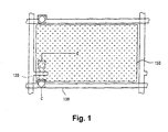
- Fig. 1 is a plan view showing one pixel portion of a conventional active matrix reflective LCD in which a thin film transistor (TFT) is provided for each pixel.
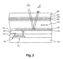
- Fig. 2 schematically shows a cross sectional configuration of the reflective LCD taken along line C-C of Fig. 1.
- the reflective LCD comprises a first substrate 100 and a second substrate 200 which are adhered to each other with a predetermined gap therebetween and a liquid crystal layer 300 sealed between the first and second substrates.
- a glass or plastic substrate is used for the first and second substrate 100 and 200, while a transparent substrate is used as the second substrate 200 located on the viewer side, at least in this example.
- a thin film transistor (TFT) 110 is formed for each pixel.
- TFT 110 for example, a drain region in an active layer 120 is connected with a data line 136 which supplies a data signal to each pixel via a contact hole formed in an inter-layer insulating film 134.
- a source region of the TFT 110 is connected with a first electrode (pixel electrode) 150 which is individually formed for each pixel via a contact hole formed to penetrate the inter-layer insulating film 134 and a planarization insulating film 138.
- a material having a reflective function such as Al, Ag, or the like, is employed as the first electrode 150.
- an alignment film 160 is formed so as to control the initial alignment of the liquid crystal layer 300.
- a color filter (R, G, B) 210 is formed, and a transparent electrode 250 comprising a transparent conductive material such as ITO (Indium Tin Oxide) is formed on the color filter 210. Further, on the transparent electrode 250, an alignment film 260 which is similar to the alignment film 160 on the first substrate side is formed.
- the liquid crystal is driven by an alternating voltage so as to prevent image persistence.
- transmissive LCDs as both the first electrode on the first substrate and the second electrode on the second substrate should be transparent, ITO is used as a material for both electrodes . Consequently, for AC driving of the liquid crystal, each of the first and second electrodes can apply a positive or negative voltage on substantially the same conditions.
- asymmetricity of the electrical characteristics of the first and second electrodes relative to the liquid crystal layer 300 is one cause. It is believed that such asymmetricity results from a significant difference between a work function of 4.7eV ⁇ 5.2eV for the transparent metal oxide such as ITO used in the second electrode 250 and a work function of 4.2eV ⁇ 4.3eV for the metal such as Al used in the first electrode 150. Such a difference in the work function would cause there to be a difference of a charge actually induced on the liquid crystal interface via the alignment films 160 and 260, when the same voltage is applied to each electrode.
- Reflective LCDs in which ITO is used for both the first and second electrodes as in transmissive LCDs and a reflector is separately provided on the outer side of the first electrode (on the side of the first electrode not facing the liquid crystal) are conventionally known.
- a reflector is thus provided on the outer side of the fist substrate, however, the length of a light path is increased by an amount corresponding to the thickness of the transparent first electrode 150 and of the transparent first substrate, thereby making the display quality likely to deteriorate due to parallax. Consequently, in reflective LCDs which demand high display quality, a reflective electrode is employed as a pixel electrode, and it is therefore impossible to reduce the drive frequency so as to achieve lower power consumption, because flicker or the like is generated at the lower drive frequency, as described above.
- transflective LCDs having both a reflective functionality and a transmissive functionality are proposed and have attracted attention as display devices that are viewable both under bright light, such as outdoors on a sunny day, and under dark. conditions.
- a transparent electrode such as one made of ITO is utilized, similar as in a transmissive LCD, for realizing the transmissive functionality and a reflective electrode having a superior reflective characteristic, such as one made of Al, is used for realizing reflective functionality.
- a transparent electrode such as one made of ITO
- a reflective electrode having a superior reflective characteristic such as one made of Al
- transflective LCDs are created by first layering a transparent electrode similar to that found in transmissive LCDs, and then layering a reflective electrode on a partial region on the transparent electrode. With such an order of layering, manufacturing a transflective LCD can be accomplished merely by adding a process for forming a reflective electrode after formation of a transparent electrode using a method for manufacturing a transmissive LCD.
- the connection between the switching element and the transparent electrode can be realized through processes similar to those in the transmissive LCDs and the reflective electrode formed on the transparent electrode is electrically connected to the transparent electrode. Therefore, it is possible to form, in each pixel, a pixel electrode having a reflective functionality and a transmissive functionality wherein the transparent electrode and the reflective electrode partially covering the transparent electrode are electrically integrated, through processes similar to those for transmissive LCDs.
- the reflective electrode in the reflective region on the first substrate side is placed on a side facing the liquid crystal layer.
- This configuration suffers from a problem in that, because of the difference in the work functions between the reflective electrode on the first substrate side and the transparent second electrode on the second substrate side, flicker or the like may occur due to the asymmetry of the AC driving of liquid crystal, similar as in the reflective LCDs described earlier.
- each pixel contains a region wherein the reflective electrode is formed on a side facing the liquid crystal layer and a region wherein the reflective electrode is not formed.
- the generation processes for flicker and for image persistence in the liquid crystal layer differ between the reflective region and the transmissive region, there is a possibility that the occurrence of defects may become more noticeable such as, for example, image persistence occurring only in a portion of the liquid crystal layer.
- the reflective mode is switched to or from the transmissive mode, the display quality may change dramatically. Such rapid changes and locational variations in display quality are not desirable in a display device.
- any difference in the optical characteristics of the reflective region and the transmissive region must also be considered. At present, however, adjustments in consideration of these differences are not optimized and efficient means for performing these adjustments are desired.
- the present invention was conceived to solve the above problem and an advantage of the present invention is that the electrical characteristics of the first and second electrodes for applying a drive voltage to the liquid crystal layer are matched in a transflective liquid crystal display apparatus so as to realize a liquid crystal display apparatus with a reflective functionality. and a transmissive functionality and having a lower occurrence of flicker, a lower influence of parallax, a high display quality, and a low power consumption.
- a liquid crystal display apparatus having a liquid crystal layer sealed between a first substrate having a first electrode and a second substrate having a second electrode, wherein the first substrate comprises a reflective layer formed only in a subregion within a pixel region, for reflecting light transmitted and incident through the second substrate and the second electrode to the liquid crystal layer; a transparent conductive material is used for the first electrode; the first electrode made of transparent conductive material is layered to cover a transmissive region within a pixel region and over the reflective layer in a reflective region within the pixel region to directly cover the reflective layer; a twist angle which is a difference between the alignment direction of liquid crystal at the side of the first electrode and the alignment direction of liquid crystal at the side of the second electrode is set to 60° or greater; and, in a pixel region, a gap dr which is defined as a distance between the first electrode and the second electrode in the reflective region is approximately equal to a gap dt, which is defined
- a first electrode made of a transparent conductive material is provided on the first substrate side on a side facing the liquid crystal layer, both in the reflective region wherein a reflective layer is formed and in the transmissive region and a reflective layer is formed below the first electrode only in the reflective region.
- the transparent conductive material for the first electrode a material having a work function similar to, for example, a transparent conductive material used for the second electrode.
- a liquid crystal display apparatus having a liquid crystal layer sealed between a first substrate having a first electrode and a second substrate having a second electrode, wherein the first substrate comprises a reflective layer formed only in a subregion within a pixel region, for reflecting light transmitted and incident through the second substrate and the second electrode to the liquid crystal layer; a transparent conductive material is used for the first electrode; the first electrode made of the transparent conductive material is layered to cover a transmissive region within a pixel region and over the reflective layer in a reflective region within the pixel region to directly cover the reflective layer; a twist angle which is a difference between the alignment direction of liquid crystal at the side of the first electrode and the alignment direction of liquid crystal at the side of the second electrode is set to 80° or less; a gap adjustment layer is formed below the reflective layer formed in the reflective region; and in a pixel region, a difference between a gap dr which is defined as a distance between the first electrode and the second electrode in the reflective region and a gap
- the gaps dr and dt can be set such that the gap dr is approximately 0.4 - 0.6 times the gap dt.
- a difference between the work function of the transparent conductive material for the first electrode and the work function of a transparent conductive material for the second electrode formed on the second substrate side on a side facing the liquid crystal layer is set to 0.5 eV or less.
- a switching element is formed for each pixel over the first substrate; the reflective layer is formed on an insulating film which covers the switching element, the reflective layer being insulated from the switching element; and a connecting metal layer is formed within a contact hole formed in the insulating film covering the switching element, and the switching element and the first electrode are electrically connected through the connecting metal layer.
- Fig. 3 shows a portion of a planer structure of a first substrate side in a case where a transflective active matrix LCD is employed as a transflective LCD according to the embodiment.
- Fig. 4A schematically shows a cross sectional structure around a TFT in a pixel along the line A-A of Fig. 3 and
- Fig. 4B schematically shows an overall cross sectional structure of the LCD along the line B-B of Fig. 3.
- an active matrix LCD a plurality of pixels are provided in a matrix form within a display region and a switching element such as a TFT is provided corresponding to each pixel.
- the switching element is formed for each pixel on one of a first substrate side and a second substrate side, for example, in the illustrated structure, on the side of the first substrate 100.
- a pixel electrode (first electrode) 50 which is formed in an individual pattern is connected to the switching element.
- a transparent substrate such as glass is used. Similar to the conventional art, on the side of the second substrate 200 opposing the first substrate, a color filter 210 is formed for a color type structure and a second electrode 250 which is made of a transparent conductive material is formed on the color filter 210. As a transparent conductive material for the second electrode 250, IZO (Indium Zinc Oxide) or ITO is used. In an active matrix device, the second electrode 250 is formed as a common electrode for all pixels. An alignment film 260 made of polyimide or the like is formed on the second electrode 250.
- a structure of electrodes is employed such that the electrical characteristics, with respect to a liquid crystal layer 300, of the first substrate side is matched with those of the second substrate side.
- a first electrode 50 made of a transparent conductive material having a similar work function as the second electrode 250, that is, a material similar to the second electrode 250, such as IZO or ITO is formed and layered immediately below an alignment film over the first substrate to cover almost the entire region of a pixel region.
- a reflective region wherein light incident from the side of the second substrate 200 is reflected to the liquid crystal layer 300 and a transmissive region wherein light generated by a backlight or the like is transmitted from the first substrate 100 side towards the second substrate side are formed within a pixel region.
- a reflective layer 44 which is directly covered by the first electrode 50 and for reflecting the incident light from the second substrate side is formed.
- the transmissive region the reflective layer 44 is opened and is not present, and the first electrode 50 is formed directly over a planarization insulating film 38 which will be described below.
- first electrode 50 By forming the first electrode 50 of the same material as used for the second electrode 250, electrodes having the same work function sandwich the liquid crystal layer 300, via the alignment layers 60 and 260, respectively, so that the liquid crystal layer 300 can be AC driven by the first and second electrodes 50 and 250 with very good symmetry.
- the work functions of the first and second electrodes 50 and 250 need not be completely identical and may be as approximate to each other as possible so that the liquid crystal layer 300 can be symmetrically driven.
- the difference between the work functions of the both electrodes is approximately 0.5eV or less, high quality display without flicker or image persistence in the liquid crystal layer can be achieved, even when the drive frequency for the liquid crystal is set to CFF or lower, as described above.
- IZO whose work function is 4.7eV ⁇ 5.2eV
- ITO whose work function is 4.7eV ⁇ 5.0eV
- the material used for each electrode may be selected in consideration of process properties such as transmissivity and patterning precision and manufacturing cost.
- the reflective layer 44 a material having a superior reflective characteristic such as Al, Ag, or an alloy of these (in the embodiment, an Al-Nd alloy) is used at least on the front surface (the side facing the liquid crystal layer).
- the reflective layer 44 may be a single layer of a metal material such as Al, or, alternatively, a layer of refractory metal (high melting point metal) such as Mo may be formed as a lower buffer layer which contacts the planarization insulating film 38. By forming such lower buffer layer, the contact between the reflective layer 44 and planarization insulating film 38 can be improved, and, consequently, the reliability of the element can be enhanced.
- the reflective layer 44 which is made of a conductive material such as Al, as described above, is electrically insulated from the first electrode 50 formed on the reflective layer 44 because the first electrode 50 is formed by sputtering IZO or ITO, when these materials are used. More specifically, because the reflective layer 44 made of Al, when exposed to the sputtering atmosphere, undergoes oxidation reaction on its surface and is covered with a natural oxide film. Therefore, according to the present embodiment, rather than using this reflective layer 44 as a first electrode which drives the liquid crystal as in the convention reflective LCD, the transparent conductive layer formed on the reflective film 44 is used as the first electrode 50 for applying a voltage in accordance with the display data to the liquid crystal 300.
- the twist angle of the liquid crystal corresponds to a difference between a direction (rubbing angle) of an initial alignment, controlled by an alignment film 60, of the liquid crystal in the substrate surface on the side of the first substrate 100 and a direction (rubbing angle) of an initial alignment, controlled by an alignment film 260, of the liquid crystal in the substrate surface on the side of the second substrate 200.
- the twist angle of liquid crystal is set at 60° or greater, for example, 63°, and more preferably 70° or greater.
- the cell gap dr in the reflective region and the cell gap dt in the transmissive region are set to be approximately equal to each other, as shown in Fig. 4B.
- the "approximate equal" relationship between the cell gaps dr and dt includes a difference in the order of the thickness of the reflective layer 44.
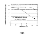
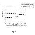
- Figs. 5 and 6 show results of evaluations of characteristics of the reflective region and for the transmissive region, respectively, with respect to the twist angle of the liquid crystal in a transflective LCD, as obtained by the applicant.
- Fig. 5 shows dependencies, on the twist angle, of the reflectance in the reflective region and of the transmittance in the transmissive region when the same voltage is applied to the liquid crystal.
- the reflectance in the reflective region only shows a small degree of dependence on the twist angle and sufficient reflectance can be obtained over almost the entire range of twist angles.
- the transmittance in the transmissive region is reduced as the twist angle is increased. Therefore, from the results of Fig.
- Fig. 6 shows dependencies, on the twist angle, of ⁇ nd which yield optimum reflectance and optimum transmittance (hereinafter referred to simply as "optimum ⁇ nd").
- ⁇ n denotes an anisotropy of index of refraction of liquid crystal
- d denotes the cell gap [distance between the first electrode and the second electrode] .
- the twist angle is approximately 60°, and more preferably, 70° or greater, the optimum ⁇ nd for the reflective region approximately coincides with the optimum ⁇ nd for the transmissive region.
- the change in the optimum ⁇ nd for the transmissive region is small, but the optimum ⁇ nd for the reflective region begins to decrease as the twist angle is reduced to a value of less than approximately 70°.
- the values for the gap d, etc. is not limited to the values derived from Fig. 6, but, as it can be seen from Fig. 6 that when the twist angle is approximately 60° or greater or, more preferably, approximately 70° or greater, the optimum ⁇ nd for the cell gap dt in the transmissive region and the optimum ⁇ nd for the cell gap dr in the reflective region are almost equal, by setting, as shown in Figs. 4A and 4B, the cell gaps dt and dr to approximate equal values corresponding to the optimum ⁇ nd, it is possible to simultaneously achieve maximum reflectance and maximum transmittance.
- the twist angle is less than approximately 80°, more specifically, less than approximately 70°
- the optimum ⁇ nd for the transmissive region changes by a small amount, from approximately 0.26 to 0.275, whereas the optimum ⁇ nd for the reflective region is significantly reduced from 0.255 at a twist angle of 70° to 0.14 at a twist angle of 0°.
- the parameter related to the liquid crystal that is, ⁇ n
- the gap between the first electrode 50 and the second electrode 250 must be determined such that the cell gaps dr and dt which differ from each other are achieved in the transmissive region and in the reflective region corresponding to the respective values of the optimum ⁇ nd.
- the gap dr in the reflective region must be set to a value less than the gap dt in the transmisssive region.
- the optimum gap [dt] in the transmissive region is 3.37 ⁇ m and the optimum gap [dr] in the reflective region is 1.94 ⁇ m. More generally, when the twist angle is 0°, it can be seen that the gap dr in the reflective region should be set to be approximately 1/2 of, for example, 0.4 times - 0.6 times, the gap dt in the transmissive region. From the results shown in Fig. 5, it can be seen that the transmittance, which shows a dependence on the twist angle, can be increased in the transmissive region by reducing the twist angle. Therefore, by decreasing the twist angle and designing the cell gaps to have varied reflective and transmissive regions, it is possible to achieve a higher transmittance and a higher reflectivity.
- Figs. 7A and 7B show a structure commonly known as a "multi-gap structure" in which the twist angle is 80° or less and the cell gaps in the reflective region and in the transmissive region are set to suitable values.
- Fig. 7A schematically shows the cross sectional structure of the first substrate side along the line A-A of Fig. 3 and
- Fig. 7B schematically shows the cross sectional structure of the LCD along the line B-B of Fig. 3.
- Figs. 7A and 7B correspond respectively to Figs. 4A and 4B described above with a difference that a multi-gap structure is employed and gaps in the reflective region and in the transmissive region differ from each other.
- the twist angle is 80° or less
- a structure wherein the gap dr in the reflective region is smaller than the gap dt in the transmissive region is necessary.
- This structure is achieved by forming a gap adjustment layer having a desired thickness below the reflective layer 44.
- the planarization insulating layer 38 is also utilized as the gap adjustment layer.
- the planarization insulating film 38 is formed such that it is thick in the reflective region and thin in the transmissive region corresponding to the desired values for the gaps dr and dt.
- Fig. 7A the planarization insulating film 38 is formed such that it is thick in the reflective region and thin in the transmissive region corresponding to the desired values for the gaps dr and dt.
- the gaps are adjusted by removing the planarization insulating layer 38 in the transmissive region and leaving the planaization insulating layer 38 in the reflective region corresponding to the desired values for the gaps dr and dt.
- a structure for reliably connecting the first electrode 50 and the corresponding TFT 110 in the transflective active matrix LCD according to the embodiment and a method for manufacturing such a structure will be explained referring to Figs. 3, 4A, 4B, 7A, and 7B.
- the TFT 110 and the corresponding first electrode 50 can be formed through similar steps which will be described below.
- a top gate type TFT is employed as the TFT 110 and polycrystalline silicon (p-Si) obtained through polycrystallization of amorphous silicon (a-Si) by laser annealing is used as an active layer 20.
- the TFT 110 is not limited to a top gate type TFT having a p-Si active layer, and may be of a bottom gate type, may have an a-Si active layer, or both.
- the impurities to be doped into a source region 20s and a drain region 20d of the active layer 20 of the TFT 110 may be either n conductive type impurities or p conductive type impurities.
- an n-ch type TFT 110 is employed in which n conductive type impurities such as phosphorus are doped.
- the active layer 20 of the TFT 110 is covered by a gate insulating film 30, and a gate electrode 32 made of Cr or the like and which also functions as a gate line is formed on the gate insulating film 30.
- the impurities as described above are doped into the active layer 20 with the gate electrode 32 functioning as a mask so that a source region 20s and a drain region 20d are formed and a channel region 20c which is not doped with the impurities is formed.
- an interlayer insulating film 34 is formed to entirely cover the TFT 110, contact holes are formed in the interlayer insulating film 34, and an electrode material is formed such that a source electrode 40 is connected to the source region 20s of the p-Si active layer and a drain electrode 36 is connected to the drain region 20d of the p-Si active layer 20 through respective contact holes.
- the drain electrode 36 also functions as a data line for supplying a data signal corresponding to the display content to each TFT 110.
- the source electrode 40 is connected to the first electrode 50, which is a pixel electrode as will be described below.
- a planarization insulating layer 38 made of a resin material such as an acrylic resin is formed to entirely cover the substrate.
- the planarization insulating layer 38 is formed to a thickness necessary for the reflective region, and then the thickness of the planarization insulating layer 38 is reduced or the planarization insulating layer 38 is completely removed in the transmissive region through etching.
- the planarization insulating layer 38 entirely covering the substrate to a thickness necessary to planarize the upper surface of the substrate and to selectively form a gap adjustment layer having a necessary thickness in the reflective region.
- the gap adjustment layer is formed using a material which makes the upper surface planer similar to the material for the planarization insulating layer 38, it is possible to maintain the flatness of the reflective surface of the reflective layer 44 formed above the gap adjustment layer, but the material for the gap adjustment layer is not limited to such material and any other insulating material may be used.
- a contact hole is formed in the region of the planarization insulating layer 38 corresponding to the region where the source electrode 40 is formed.
- a connecting metal layer 42 is formed in the contact hole and the source electrode 40 and the metal layer 42 are connected.
- a metal material such as Mo for the metal layer 42.
- the source electrode 40 may be omitted, and in this case, the metal layer 42 contacts the silicon active layer 20 of the TFT 110.
- a metal such as Mo can establish a superior ohmic contact with such semiconductor material.
- a reflective material layer for the reflective layer, having a superior reflective characteristics such as an Al-Nd alloy or Al is layered entirely over the substrate through deposition or sputtering.
- the layered reflective material layer is etched and removed in regions around the source region (formation region of the metal layer 42) of the TFT 110 and in the transmissive region so that the reflective material layer does not interfere with the connection between the metal layer 42 and the first electrode 50 which will be formed later.
- a reflective layer 44 having a pattern as shown in Fig. 3 is formed in the reflective region of each pixel.
- the reflective layer 44 is also actively formed in the region above the channel of the TFT 110, as shown in Fig. 3, in order to prevent generation of leak currents due to light irradiating onto the TFT 110 (in particular, the channel region 20c), and to broaden the region which can reflect light (that is, the display region) to the extent possible.
- the metal layer 42 made of Mo or the like has a sufficient thickness (for example, 0.2 ⁇ m) and a sufficient tolerance to the etching solution. Therefore, even when the reflective layer 44 over the metal layer 42 is removed by etching, the metal layer 42 is not completely removed and remains in the contact hole. In many cases, as a material similar to that for the reflective layer 44 (such as Al) is used for the source electrode 40 or the like, if the metal layer 42 is not present, the source electrode 40 may be corroded by the etching solution for the reflective layer 44 and disconnection or the like may occur. By providing the metal layer 42 as in the embodiment, it is possible to tolerate the patterning of the reflective layer 44 and a superior electrical connection with the source electrode 40 can be maintained.
- a transparent conductive layer is layered through sputtering to entirely cover the substrate including the reflective layer 44.
- the surface of the reflective layer 44 made of Al or the like as described above is covered by an insulating natural oxide film, but the surface of the refractory metal such as Mo is not oxidized even when exposed to the sputtering atmosphere. Therefore, an ohmic contact can be achieved between the metal layer 42 exposed in the contact region and the transparent conductive layer for the first electrode which is layered on the metal layer 42.
- the transparent conductive layer is patterned, after it is formed, independently for each pixel, and, in each pixel region, into a common shape for the reflective region and the transmissive region.
- a pixel electrode (first electrode) 50 is formed.
- an alignment film 60 made of polyimide or the like is formed to entirely cover the substrate and the first substrate side is completed.
- the first substrate 100 and a second substrate 200 to which the elements are formed up to the alignment film 260 are affixed at peripheral sections of the substrates with a predetermined gap therebetween and liquid crystal are sealed into the space between the substrates to form a liquid crystal display apparatus.
- the connecting metal layer 42 for connecting the TFT 110 and the first electrode 50 can maintain a preferable connection with the source electrode 40, even when the source electrode 40 has a multi-layered structure in which an Al layer is provided between refractory metal layers such as Mo.
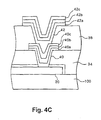
- An example of such a multi-layer structure of the source electrode 40 is shown in Fig. 4C which has a structure of Mo layer/Al layer/Mo layer layered, in that order, from the side of the active layer 20. Because a Mo layer is formed on the side of the active layer 20 made of p-Si, it is possible to prevent defect generation in the active layer caused by Si atoms moving into an Al layer.
- the connecting metal layer 42 may have a multi-layered structure similar to the source electrode 40 described above.
- the multi-layered structure for example, a three-layer structure of layer of a refractory metal such as Mo/conductive layer such as Al/layer of a refractory metal such as Mo or a two-layered structure of conductive layer such as Al/layer of a refractory metal such as Mo layered from the bottom to the top may be employed.
- the source electrode 40 provided below the metal layer 42 may have a multi-layered structure as described above or a single layer structure of Al or the like.
- a metal layer 42 having a three-layered structure or a two-layered structure as described above.
- the metal layer 42 must tolerate etching of the reflective layer 44 and stably maintain electrical connection characteristics without formation of an insulating film on the surface when the first electrode 50 is formed, and therefore it is preferable that a refractory metal layer is formed at least on the side of the surface contacting the first electrode 50.
- a transflective LCD even when a reflective layer must be selectively formed on a reflective region of one of the substrate sides, it is possible to place a first electrode and a second electrode having similar characteristics in equivalent positions with respect to a liquid crystal layer. Therefore, it is possible to more symmetrically AC drive the liquid crystal. As a result, even when the driving frequency of the liquid crystal is set, for example, to a value less than the CFF, it is possible to realize a transflective LCD which can display at a high quality and wherein no flicker nor image persistence occurs.
- the cell gaps in the reflective region and in the transmissive region corresponding to the twist angle of the liquid crystal layer it is possible to achieve an optimum reflectance and an optimum transmittance respectively in the reflective region and in the transmissive region.
Landscapes
- Physics & Mathematics (AREA)
- Nonlinear Science (AREA)
- Mathematical Physics (AREA)
- Chemical & Material Sciences (AREA)
- Crystallography & Structural Chemistry (AREA)
- General Physics & Mathematics (AREA)
- Optics & Photonics (AREA)
- Liquid Crystal (AREA)
Abstract
Description
Claims (6)
- A liquid crystal display apparatus having a liquid crystal layer sealed between a first substrate having a first electrode and a second substrate having a second electrode, wherein
the first substrate comprises a reflective layer formed only in a subregion within a pixel region, for reflecting light transmitted and incident through the second substrate and the second electrode to the liquid crystal layer;
a transparent conductive material is used for the first electrode;
the first electrode made of the transparent conductive material is layered to cover a transmissive region within a pixel region and over the reflective layer in a reflective region within the pixel region to directly cover the reflective layer;
a twist angle which is a difference between the alignment direction of liquid crystal at the side of the first electrode and the alignment direction of liquid crystal at the side of the second electrode is set to 60° or greater; and
in a pixel region, a gap dr which is defined as a distance between the first electrode and the second electrode in the reflective region is approximately equal to a gap dt which is defined as a distance between the first electrode and the second electrode in the transmissive region. - A liquid crystal display apparatus having a liquid crystal layer sealed between a first substrate having a first electrode and a second substrate having a second electrode, wherein
the first substrate comprises a reflective layer formed only in a subregion within a pixel region, for reflecting light transmitted and incident through the second substrate and the second electrode to the liquid crystal layer;
a transparent conductive material is used for the first electrode;
the first electrode made of the transparent conductive material is layered to cover a transmissive region within a pixel region and over the reflective layer in a reflective region within the pixel region to directly cover the reflective layer;
a twist angle which is a difference between the alignment direction of liquid crystal at the side of the first electrode and the alignment direction of liquid crystal at the side of the second electrode is set to 80° or less;
a gap adjustment layer is formed below the reflective layer formed in the reflective region; and
in a pixel region, a difference between a gap dr which is defined as a distance between the first electrode and the second electrode in the reflective region and a gap dt which is defined as a distance between the first electrode and the second electrode in the transmissive region is greater than the thickness of the reflective layer. - A liquid crystal display apparatus according to claim 2, wherein
when the twist angle is approximately 0°, a gap dt which is defined as the distance between the first electrode and the second electrode in the transmissive region and a gap dr which is defined as the distance between the first electrode and the second electrode in the reflective region within the pixel region satisfy a condition that dr is approximately 0.4 times - 0.6 times dt. - A liquid crystal display apparatus according to any one of claims 1 to 3, wherein
a difference between a work function of the transparent conductive material for the first electrode and a work function of a transparent conductive material for the second electrode formed on the second substrate side over a surface facing the liquid crystal layer is 0.5 eV or less. - A liquid crystal display apparatus according to any one of claims 1 to 4, wherein
a switching element is formed for each pixel over the first substrate;
the reflective layer is placed on an insulating film which covers the switching element, the reflective layer being insulated from the switching element; and
a connecting metal layer is formed within a contact hole formed in the insulating film covering the switching element and the switching element and the first electrode are electrically connected through the connecting metal layer. - A liquid crystal display apparatus according to any one of claims 1 to 5, wherein the driving frequency of the liquid crystal layer for each pixel is 60 Hz or less.
Applications Claiming Priority (2)
| Application Number | Priority Date | Filing Date | Title |
|---|---|---|---|
| JP2001401051 | 2001-12-28 | ||
| JP2001401051 | 2001-12-28 |
Publications (3)
| Publication Number | Publication Date |
|---|---|
| EP1326130A2 true EP1326130A2 (en) | 2003-07-09 |
| EP1326130A3 EP1326130A3 (en) | 2003-10-29 |
| EP1326130B1 EP1326130B1 (en) | 2007-02-14 |
Family
ID=19189716
Family Applications (1)
| Application Number | Title | Priority Date | Filing Date |
|---|---|---|---|
| EP02259010A Expired - Lifetime EP1326130B1 (en) | 2001-12-28 | 2002-12-30 | Liquid crystal display apparatus |
Country Status (6)
| Country | Link |
|---|---|
| US (2) | US20030151712A1 (en) |
| EP (1) | EP1326130B1 (en) |
| KR (1) | KR100513610B1 (en) |
| CN (2) | CN100363789C (en) |
| DE (1) | DE60218126D1 (en) |
| TW (1) | TWI296062B (en) |
Cited By (3)
| Publication number | Priority date | Publication date | Assignee | Title |
|---|---|---|---|---|
| WO2004025617A3 (en) * | 2002-09-12 | 2004-06-03 | Koninkl Philips Electronics Nv | Transflective liquid crystal display with reduced flicker |
| WO2006087685A1 (en) * | 2005-02-21 | 2006-08-24 | Koninklijke Philips Electronics N.V. | Lcd with reduced flicker and a method for manufacturing thereof |
| US11269214B2 (en) | 2005-12-28 | 2022-03-08 | Semiconductor Energy Laboratory Co., Ltd. | Display device and manufacturing method thereof |
Families Citing this family (24)
| Publication number | Priority date | Publication date | Assignee | Title |
|---|---|---|---|---|
| CN1392964A (en) * | 2000-09-27 | 2003-01-22 | 松下电器产业株式会社 | Transreflective liquid crystal display |
| US7064799B2 (en) * | 2002-07-10 | 2006-06-20 | Nec Lcd Technologies, Ltd. | Semi-transmissive-type liquid crystal display device and method for manufacturing same |
| US7646459B2 (en) * | 2003-12-26 | 2010-01-12 | Sharp Kabushiki Kaisha | Liquid crystal display device |
| JP2005275102A (en) * | 2004-03-25 | 2005-10-06 | Nec Lcd Technologies Ltd | Transflective liquid crystal display device and manufacturing method thereof |
| US7573551B2 (en) * | 2004-05-21 | 2009-08-11 | Sanyo Electric Co., Ltd. | Transflective liquid crystal display device and color liquid crystal display device |
| CN100385303C (en) * | 2004-06-14 | 2008-04-30 | 夏普株式会社 | Liquid crystal display and manufacturing method thereof |
| WO2006012773A1 (en) * | 2004-08-04 | 2006-02-09 | Quanta Display Inc. | A transflective liquid crystal display and the manufacturing method thereof |
| JP4075876B2 (en) * | 2004-09-01 | 2008-04-16 | セイコーエプソン株式会社 | Electro-optical device and electronic apparatus |
| JP4016977B2 (en) * | 2004-09-03 | 2007-12-05 | セイコーエプソン株式会社 | Liquid crystal display device, electronic equipment |
| JP2006126551A (en) * | 2004-10-29 | 2006-05-18 | Hitachi Displays Ltd | Liquid crystal display |
| JP2006235012A (en) * | 2005-02-23 | 2006-09-07 | Hitachi Displays Ltd | Liquid crystal display |
| KR20070062689A (en) * | 2005-12-13 | 2007-06-18 | 삼성전자주식회사 | Liquid crystal display and driving method thereof |
| TWI333112B (en) | 2006-03-16 | 2010-11-11 | Au Optronics Corp | Liquid crystal driving electrode and liquid crystal display using the same |
| TWI337285B (en) | 2006-04-25 | 2011-02-11 | Au Optronics Corp | Active device array substrate, color filter substrate and respective manufacturing methods thereof |
| US7675097B2 (en) * | 2006-12-01 | 2010-03-09 | International Business Machines Corporation | Silicide strapping in imager transfer gate device |
| KR101264717B1 (en) * | 2007-03-26 | 2013-05-16 | 엘지디스플레이 주식회사 | Liquid Display Pnel of Transflective Type And Fabricating Method Thereof |
| TWI342978B (en) * | 2007-10-24 | 2011-06-01 | Au Optronics Corp | Active device array substrate, pixel structure thereof and driving method thereof |
| KR101631045B1 (en) | 2008-02-29 | 2016-06-15 | 메르크 파텐트 게엠베하 | Alignment film for liquid crystals obtainable by direct particle beam deposition |
| WO2009146061A2 (en) * | 2008-04-02 | 2009-12-03 | Johnson Paul K | Pulsed led illumination to save energy |
| JP5663883B2 (en) * | 2010-01-27 | 2015-02-04 | セイコーエプソン株式会社 | Liquid crystal device and method for manufacturing liquid crystal device |
| KR102288820B1 (en) * | 2015-01-16 | 2021-08-11 | 엘지이노텍 주식회사 | Touch window and touch device |
| CN105549249A (en) * | 2016-02-23 | 2016-05-04 | 武汉华星光电技术有限公司 | Liquid crystal display panel and mobile phone |
| CN107505764A (en) * | 2017-09-28 | 2017-12-22 | 重庆秉为科技有限公司 | Semi-penetration, semi-reflective liquid crystal display |
| CN109065582B (en) * | 2018-08-02 | 2022-02-15 | 京东方科技集团股份有限公司 | Array substrate, display panel and display device |
Family Cites Families (32)
| Publication number | Priority date | Publication date | Assignee | Title |
|---|---|---|---|---|
| US5414442A (en) * | 1991-06-14 | 1995-05-09 | Semiconductor Energy Laboratory Co., Ltd. | Electro-optical device and method of driving the same |
| CN1560691B (en) * | 1992-08-27 | 2010-05-26 | 株式会社半导体能源研究所 | Semiconductor device, method of manufacturing the same, and active matrix display |
| US5592190A (en) * | 1993-04-28 | 1997-01-07 | Canon Kabushiki Kaisha | Liquid crystal display apparatus and drive method |
| ATE169776T1 (en) * | 1993-07-13 | 1998-08-15 | Actron Entwicklungs Ag | ANTENNA DEVICE |
| JPH07321328A (en) * | 1994-05-27 | 1995-12-08 | Hitachi Ltd | Thin film transistor driven liquid crystal display device and method of manufacturing the same |
| JPH09113931A (en) * | 1995-10-16 | 1997-05-02 | Sharp Corp | Liquid crystal display |
| TW409194B (en) * | 1995-11-28 | 2000-10-21 | Sharp Kk | Active matrix substrate and liquid crystal display apparatus and method for producing the same |
| JP3191085B2 (en) * | 1996-01-29 | 2001-07-23 | 株式会社日立製作所 | Reflective liquid crystal display element and liquid crystal display device |
| JPH1054995A (en) * | 1996-06-06 | 1998-02-24 | Pioneer Electron Corp | Reflective liquid crystal display |
| US6104450A (en) * | 1996-11-07 | 2000-08-15 | Sharp Kabushiki Kaisha | Liquid crystal display device, and methods of manufacturing and driving same |
| US5764324A (en) * | 1997-01-22 | 1998-06-09 | International Business Machines Corporation | Flicker-free reflective liquid crystal cell |
| US6195140B1 (en) * | 1997-07-28 | 2001-02-27 | Sharp Kabushiki Kaisha | Liquid crystal display in which at least one pixel includes both a transmissive region and a reflective region |
| JPH1197182A (en) * | 1997-09-24 | 1999-04-09 | Pioneer Electron Corp | Luminous display panel |
| JPH11109406A (en) * | 1997-09-30 | 1999-04-23 | Sanyo Electric Co Ltd | Display device and manufacturing method thereof |
| US6281952B1 (en) * | 1997-12-26 | 2001-08-28 | Sharp Kabushiki Kaisha | Liquid crystal display |
| WO1999053368A1 (en) * | 1998-04-08 | 1999-10-21 | Seiko Epson Corporation | Liquid crystal display and electronic device |
| US6693698B2 (en) * | 1998-07-22 | 2004-02-17 | Koninklijke Philips Electronics N.V. | Display device |
| US6236440B1 (en) * | 1998-07-22 | 2001-05-22 | U.S. Philips Corporation | Display device in which one of the two electrodes of a pixel is coated with a dipole material to equalize the electrode work functions |
| EP1026652B1 (en) * | 1998-07-27 | 2005-01-26 | Seiko Epson Corporation | Arrangement of spacer beads in the seal of an electro-optic display to prevent damage to underlying conductors |
| EP1074874A4 (en) * | 1999-02-23 | 2004-07-28 | Citizen Watch Co Ltd | Liquid crystal display |
| TWI251697B (en) * | 1999-05-26 | 2006-03-21 | Matsushita Electric Industrial Co Ltd | Liquid crystal display element and producing method thereof |
| TW548484B (en) * | 1999-07-16 | 2003-08-21 | Seiko Epson Corp | Liquid crystal display device, electronic apparatus and substrate for liquid crystal device |
| KR100312328B1 (en) * | 1999-08-06 | 2001-11-03 | 구본준, 론 위라하디락사 | Transflective liquid crystal display device |
| JP3670577B2 (en) * | 2000-01-26 | 2005-07-13 | シャープ株式会社 | Liquid crystal display device and manufacturing method thereof |
| JP3766926B2 (en) * | 2000-04-28 | 2006-04-19 | シャープ株式会社 | Display device driving method, display device using the same, and portable device |
| US6608449B2 (en) * | 2000-05-08 | 2003-08-19 | Semiconductor Energy Laboratory Co., Ltd. | Luminescent apparatus and method of manufacturing the same |
| JP4278834B2 (en) * | 2000-06-02 | 2009-06-17 | 株式会社日立製作所 | Liquid crystal display device and manufacturing method thereof |
| JP3824889B2 (en) * | 2000-07-14 | 2006-09-20 | セイコーエプソン株式会社 | Color filter substrate, liquid crystal device, and manufacturing method thereof |
| JP2002162645A (en) * | 2000-09-14 | 2002-06-07 | Sony Corp | Transflective liquid crystal display |
| KR100397399B1 (en) * | 2001-02-22 | 2003-09-13 | 엘지.필립스 엘시디 주식회사 | transflective liquid crystal display and manufacturing method thereof |
| TWI255375B (en) * | 2003-04-25 | 2006-05-21 | Sanyo Electric Co | Display device |
| JP2005092122A (en) * | 2003-09-19 | 2005-04-07 | Nec Corp | Thin film transistor substrate and its manufacturing method |
-
2002
- 2002-12-06 TW TW091135389A patent/TWI296062B/en not_active IP Right Cessation
- 2002-12-27 US US10/330,998 patent/US20030151712A1/en not_active Abandoned
- 2002-12-27 KR KR10-2002-0084945A patent/KR100513610B1/en not_active Expired - Fee Related
- 2002-12-30 DE DE60218126T patent/DE60218126D1/en not_active Expired - Lifetime
- 2002-12-30 EP EP02259010A patent/EP1326130B1/en not_active Expired - Lifetime
- 2002-12-30 CN CNB2004100570336A patent/CN100363789C/en not_active Expired - Fee Related
- 2002-12-30 CN CNB021600376A patent/CN1186803C/en not_active Expired - Fee Related
-
2006
- 2006-08-23 US US11/508,712 patent/US20060285036A1/en not_active Abandoned
Cited By (4)
| Publication number | Priority date | Publication date | Assignee | Title |
|---|---|---|---|---|
| WO2004025617A3 (en) * | 2002-09-12 | 2004-06-03 | Koninkl Philips Electronics Nv | Transflective liquid crystal display with reduced flicker |
| WO2006087685A1 (en) * | 2005-02-21 | 2006-08-24 | Koninklijke Philips Electronics N.V. | Lcd with reduced flicker and a method for manufacturing thereof |
| US11269214B2 (en) | 2005-12-28 | 2022-03-08 | Semiconductor Energy Laboratory Co., Ltd. | Display device and manufacturing method thereof |
| US12189232B2 (en) | 2005-12-28 | 2025-01-07 | Semiconductor Energy Laboratory Co., Ltd. | Display device and manufacturing method thereof |
Also Published As
| Publication number | Publication date |
|---|---|
| TW200301394A (en) | 2003-07-01 |
| CN100363789C (en) | 2008-01-23 |
| TWI296062B (en) | 2008-04-21 |
| KR20030057437A (en) | 2003-07-04 |
| EP1326130B1 (en) | 2007-02-14 |
| US20060285036A1 (en) | 2006-12-21 |
| DE60218126D1 (en) | 2007-03-29 |
| KR100513610B1 (en) | 2005-09-09 |
| EP1326130A3 (en) | 2003-10-29 |
| US20030151712A1 (en) | 2003-08-14 |
| CN1598651A (en) | 2005-03-23 |
| CN1186803C (en) | 2005-01-26 |
| CN1431548A (en) | 2003-07-23 |
Similar Documents
| Publication | Publication Date | Title |
|---|---|---|
| EP1326130B1 (en) | Liquid crystal display apparatus | |
| EP1324109B1 (en) | Reflective or transflective liquid crystal display and manufacturing method therefor | |
| US7502083B2 (en) | Display apparatus and manufacturing method thereof | |
| US7482746B2 (en) | Liquid crystal display apparatus having reflective layer | |
| US8531632B2 (en) | Method of manufacturing a display device with transmissive and reflective regions | |
| JP2003255378A (en) | Liquid crystal display | |
| JP3953338B2 (en) | Liquid crystal display | |
| JP4608424B2 (en) | Liquid crystal display device and manufacturing method thereof | |
| JP2003255399A (en) | Liquid crystal display | |
| US7330227B2 (en) | Transflective liquid crystal display device | |
| JP2003255377A (en) | Display device | |
| JP2007078868A (en) | Liquid crystal display device | |
| JP2007086198A (en) | Liquid crystal display and its manufacturing method |
Legal Events
| Date | Code | Title | Description |
|---|---|---|---|
| PUAI | Public reference made under article 153(3) epc to a published international application that has entered the european phase |
Free format text: ORIGINAL CODE: 0009012 |
|
| AK | Designated contracting states |
Designated state(s): AT BE BG CH CY CZ DE DK EE ES FI FR GB GR IE IT LI LU MC NL PT SE SI SK TR |
|
| AX | Request for extension of the european patent |
Extension state: AL LT LV MK RO |
|
| PUAL | Search report despatched |
Free format text: ORIGINAL CODE: 0009013 |
|
| AK | Designated contracting states |
Kind code of ref document: A3 Designated state(s): AT BE BG CH CY CZ DE DK EE ES FI FR GB GR IE IT LI LU MC NL PT SE SI SK TR |
|
| AX | Request for extension of the european patent |
Extension state: AL LT LV MK RO |
|
| 17P | Request for examination filed |
Effective date: 20040401 |
|
| AKX | Designation fees paid |
Designated state(s): DE FI FR GB IT |
|
| 17Q | First examination report despatched |
Effective date: 20050110 |
|
| GRAP | Despatch of communication of intention to grant a patent |
Free format text: ORIGINAL CODE: EPIDOSNIGR1 |
|
| GRAS | Grant fee paid |
Free format text: ORIGINAL CODE: EPIDOSNIGR3 |
|
| GRAA | (expected) grant |
Free format text: ORIGINAL CODE: 0009210 |
|
| AK | Designated contracting states |
Kind code of ref document: B1 Designated state(s): DE FI FR GB IT |
|
| PG25 | Lapsed in a contracting state [announced via postgrant information from national office to epo] |
Ref country code: FI Free format text: LAPSE BECAUSE OF FAILURE TO SUBMIT A TRANSLATION OF THE DESCRIPTION OR TO PAY THE FEE WITHIN THE PRESCRIBED TIME-LIMIT Effective date: 20070214 |
|
| REG | Reference to a national code |
Ref country code: GB Ref legal event code: FG4D |
|
| REF | Corresponds to: |
Ref document number: 60218126 Country of ref document: DE Date of ref document: 20070329 Kind code of ref document: P |
|
| EN | Fr: translation not filed | ||
| PLBE | No opposition filed within time limit |
Free format text: ORIGINAL CODE: 0009261 |
|
| STAA | Information on the status of an ep patent application or granted ep patent |
Free format text: STATUS: NO OPPOSITION FILED WITHIN TIME LIMIT |
|
| 26N | No opposition filed |
Effective date: 20071115 |
|
| PG25 | Lapsed in a contracting state [announced via postgrant information from national office to epo] |
Ref country code: DE Free format text: LAPSE BECAUSE OF FAILURE TO SUBMIT A TRANSLATION OF THE DESCRIPTION OR TO PAY THE FEE WITHIN THE PRESCRIBED TIME-LIMIT Effective date: 20070515 |
|
| PG25 | Lapsed in a contracting state [announced via postgrant information from national office to epo] |
Ref country code: IT Free format text: LAPSE BECAUSE OF FAILURE TO SUBMIT A TRANSLATION OF THE DESCRIPTION OR TO PAY THE FEE WITHIN THE PRESCRIBED TIME-LIMIT Effective date: 20070214 Ref country code: FR Free format text: LAPSE BECAUSE OF FAILURE TO SUBMIT A TRANSLATION OF THE DESCRIPTION OR TO PAY THE FEE WITHIN THE PRESCRIBED TIME-LIMIT Effective date: 20071005 |
|
| PG25 | Lapsed in a contracting state [announced via postgrant information from national office to epo] |
Ref country code: FR Free format text: LAPSE BECAUSE OF FAILURE TO SUBMIT A TRANSLATION OF THE DESCRIPTION OR TO PAY THE FEE WITHIN THE PRESCRIBED TIME-LIMIT Effective date: 20070214 |
|
| PGFP | Annual fee paid to national office [announced via postgrant information from national office to epo] |
Ref country code: GB Payment date: 20081224 Year of fee payment: 7 |
|
| GBPC | Gb: european patent ceased through non-payment of renewal fee |
Effective date: 20091230 |
|
| PG25 | Lapsed in a contracting state [announced via postgrant information from national office to epo] |
Ref country code: GB Free format text: LAPSE BECAUSE OF NON-PAYMENT OF DUE FEES Effective date: 20091230 |