EP1321998A1 - Waveguide-microstrip transition and application to HF circuit - Google Patents
Waveguide-microstrip transition and application to HF circuit Download PDFInfo
- Publication number
- EP1321998A1 EP1321998A1 EP03006544A EP03006544A EP1321998A1 EP 1321998 A1 EP1321998 A1 EP 1321998A1 EP 03006544 A EP03006544 A EP 03006544A EP 03006544 A EP03006544 A EP 03006544A EP 1321998 A1 EP1321998 A1 EP 1321998A1
- Authority
- EP
- European Patent Office
- Prior art keywords
- waveguide
- microstrip line
- circuit
- transition
- opening
- Prior art date
- Legal status (The legal status is an assumption and is not a legal conclusion. Google has not performed a legal analysis and makes no representation as to the accuracy of the status listed.)
- Granted
Links
Images


Classifications
-
- H—ELECTRICITY
- H05—ELECTRIC TECHNIQUES NOT OTHERWISE PROVIDED FOR
- H05K—PRINTED CIRCUITS; CASINGS OR CONSTRUCTIONAL DETAILS OF ELECTRIC APPARATUS; MANUFACTURE OF ASSEMBLAGES OF ELECTRICAL COMPONENTS
- H05K3/00—Apparatus or processes for manufacturing printed circuits
- H05K3/0058—Laminating printed circuit boards onto other substrates, e.g. metallic substrates
- H05K3/0061—Laminating printed circuit boards onto other substrates, e.g. metallic substrates onto a metallic substrate, e.g. a heat sink
-
- H—ELECTRICITY
- H01—ELECTRIC ELEMENTS
- H01P—WAVEGUIDES; RESONATORS, LINES, OR OTHER DEVICES OF THE WAVEGUIDE TYPE
- H01P11/00—Apparatus or processes specially adapted for manufacturing waveguides or resonators, lines, or other devices of the waveguide type
- H01P11/001—Manufacturing waveguides or transmission lines of the waveguide type
- H01P11/003—Manufacturing lines with conductors on a substrate, e.g. strip lines, slot lines
-
- H—ELECTRICITY
- H01—ELECTRIC ELEMENTS
- H01P—WAVEGUIDES; RESONATORS, LINES, OR OTHER DEVICES OF THE WAVEGUIDE TYPE
- H01P5/00—Coupling devices of the waveguide type
- H01P5/08—Coupling devices of the waveguide type for linking dissimilar lines or devices
- H01P5/10—Coupling devices of the waveguide type for linking dissimilar lines or devices for coupling balanced with unbalanced lines or devices
- H01P5/107—Hollow-waveguide/strip-line transitions
-
- H—ELECTRICITY
- H01—ELECTRIC ELEMENTS
- H01Q—ANTENNAS, i.e. RADIO AERIALS
- H01Q1/00—Details of, or arrangements associated with, antennas
- H01Q1/36—Structural form of radiating elements, e.g. cone, spiral, umbrella; Particular materials used therewith
- H01Q1/38—Structural form of radiating elements, e.g. cone, spiral, umbrella; Particular materials used therewith formed by a conductive layer on an insulating support
-
- H—ELECTRICITY
- H01—ELECTRIC ELEMENTS
- H01Q—ANTENNAS, i.e. RADIO AERIALS
- H01Q13/00—Waveguide horns or mouths; Slot antennas; Leaky-waveguide antennas; Equivalent structures causing radiation along the transmission path of a guided wave
- H01Q13/20—Non-resonant leaky-waveguide or transmission-line antennas; Equivalent structures causing radiation along the transmission path of a guided wave
- H01Q13/206—Microstrip transmission line antennas
-
- H—ELECTRICITY
- H01—ELECTRIC ELEMENTS
- H01Q—ANTENNAS, i.e. RADIO AERIALS
- H01Q9/00—Electrically-short antennas having dimensions not more than twice the operating wavelength and consisting of conductive active radiating elements
- H01Q9/04—Resonant antennas
- H01Q9/0407—Substantially flat resonant element parallel to ground plane, e.g. patch antenna
-
- H—ELECTRICITY
- H05—ELECTRIC TECHNIQUES NOT OTHERWISE PROVIDED FOR
- H05K—PRINTED CIRCUITS; CASINGS OR CONSTRUCTIONAL DETAILS OF ELECTRIC APPARATUS; MANUFACTURE OF ASSEMBLAGES OF ELECTRICAL COMPONENTS
- H05K1/00—Printed circuits
- H05K1/02—Details
- H05K1/0213—Electrical arrangements not otherwise provided for
- H05K1/0237—High frequency adaptations
-
- H—ELECTRICITY
- H05—ELECTRIC TECHNIQUES NOT OTHERWISE PROVIDED FOR
- H05K—PRINTED CIRCUITS; CASINGS OR CONSTRUCTIONAL DETAILS OF ELECTRIC APPARATUS; MANUFACTURE OF ASSEMBLAGES OF ELECTRICAL COMPONENTS
- H05K2201/00—Indexing scheme relating to printed circuits covered by H05K1/00
- H05K2201/09—Shape and layout
- H05K2201/09818—Shape or layout details not covered by a single group of H05K2201/09009 - H05K2201/09809
- H05K2201/0999—Circuit printed on or in housing, e.g. housing as PCB; Circuit printed on the case of a component; PCB affixed to housing
-
- H—ELECTRICITY
- H05—ELECTRIC TECHNIQUES NOT OTHERWISE PROVIDED FOR
- H05K—PRINTED CIRCUITS; CASINGS OR CONSTRUCTIONAL DETAILS OF ELECTRIC APPARATUS; MANUFACTURE OF ASSEMBLAGES OF ELECTRICAL COMPONENTS
- H05K3/00—Apparatus or processes for manufacturing printed circuits
- H05K3/0058—Laminating printed circuit boards onto other substrates, e.g. metallic substrates
-
- H—ELECTRICITY
- H05—ELECTRIC TECHNIQUES NOT OTHERWISE PROVIDED FOR
- H05K—PRINTED CIRCUITS; CASINGS OR CONSTRUCTIONAL DETAILS OF ELECTRIC APPARATUS; MANUFACTURE OF ASSEMBLAGES OF ELECTRICAL COMPONENTS
- H05K3/00—Apparatus or processes for manufacturing printed circuits
- H05K3/30—Assembling printed circuits with electric components, e.g. with resistor
- H05K3/32—Assembling printed circuits with electric components, e.g. with resistor electrically connecting electric components or wires to printed circuits
- H05K3/34—Assembling printed circuits with electric components, e.g. with resistor electrically connecting electric components or wires to printed circuits by soldering
- H05K3/341—Surface mounted components
Definitions
- the present invention relates to a high frequency (HF) circuit in a communication device and more specifically to a technique for bonding a circuit board to a metal chassis or case, a waveguide-microstrip line transition, a branch circuit, and a high frequency circuit incorporating these elements.
- HF high frequency
- FIG. 1 is a diagram showing an arrangement of a prior art array antenna assembly 1.
- the antenna assembly 1 comprises an dielectric substrate 10, a circuit pattern 20, a chassis 30 that holds the dielectric substrate 10 and serves as the ground, and a waveguide-microstrip line transition 40.
- the circuit pattern 20, which constitutes an array antenna includes a T branch circuit 50.
- a signal transmitted through a waveguide is passed by the transition 40 to a microstrip line of the circuit pattern 20, and further passed by the T branch circuit 50 to the right and the left portions of the array antenna.
- FIG. 2 is a schematic diagram showing an arrangement of the transition 40 of FIG. 1.
- the transition 40 comprises a ridge waveguide 42, a ridge 41 formed inside the ridge waveguide 42, and a microstrip line 21 which is formed on the dielectric substrate 10 and which is extending to (or a part of) the circuit pattern 20.
- the signal transmitted through the not-shown waveguide is converted into a transmission mode of the microstrip line 21 by the ridge 41 provided inside the waveguide 42 and transmitted to the array antenna 20.
- the degree of freedom is very low in designing a waveguide-microstrip line transition, i.e., the design parameters are limited only to the width, the length and the height of the ridge 41, this sometimes causes the width of ridge for a milliwave band to be extremely narrow. Accordingly, the height of the ridge 41 of the transition 40, which is manufactured through machining of a brass material, becomes higher as compared with the ridge 41 width, making the work difficult.
- the lack of the degree of freedom in design may disable the conversion into a microstrip line with a lower characteristic impedance and cause the problem that a too match difference between the widths of the designed ridge 41 and the microstrip line 21 leads to an unexpected deterioration in the line conversion characteristics.
- an array antenna 20 as a whole generally exhibits a narrower frequency band characteristic with an increase in the number of array elements.
- the antenna needs a beam width of about 2 degrees and accordingly a very large size.
- the resultant antenna would exhibit a very narrow frequency band characteristic, causing the band width of the antenna to be narrower than that of the radar. This is because conventional branch circuits mainly use stubs for impedance matching.
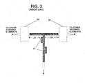
- FIG. 3 is a diagram showing an exemplary pattern of a conventional T branch circuit comprising a matching circuit that uses stubs 51 (the T branch circuit is shown as a dark area).
- Using stubs for impedance matching generally tends to narrow the frequency characteristics of the circuit. Specifically, the larger the distances (D1 and D2) between the matching circuit and circuits (22) that need matching, the narrower the frequency band of the whole circuit.
- the antenna will fail to provide a desired characteristics.
- matching by stubs while providing a desired characteristic to the antenna or the circuits having their impedance matched inevitably narrows the frequency band of the resultant circuit such as an antenna.
- the invention is directed to solving these and other problems and disadvantages of the prior art.
- a method of bonding a circuit board with a metal plate includes the steps of working the metal plate so as to have a shape that permits a fluid to form a bath in an area including a part where the circuit board is to be bonded; heating the worked metal plate to such a temperature as melt a conductive bonding material; forming a bath of the conductive bonding material in the area of the metal plate; floating the circuit board on the bath; and absorbing excessive portion of the conductive material without applying a force to the dielectric substrate.
- a circuit assembly according to just-described aspect of the invention is provided with a thin and large-area dielectric substrate with an improved earthing condition.
- a bonding agent with a low melting point, a low melting point solder, etc. may be used as conductive material.
- a branch circuit for branching a first path into at least two second paths in a high frequency circuit.
- the impedance matching between the first path and each of the branch paths is achieved by mainly using impedance transformers but by using fewest possible stub(s) in the branch circuit.
- the first path, the second paths, the impedance transformers, and the fewest possible stub(s) are arranged in symmetry with respect to a plane of symmetry that runs through the first path.
- the impedance transformers are step impedance transformers.
- a waveguide-microstrip line transition that is easy to work and low in transition loss.
- the transition comprises a fanwise tube having a first opening coupled with a waveguide and a second opening larger in size then the first opening, a first and a second wider wall of the tube spreading from the first opening toward the second opening; an end portion of a microstrip line formed on a dielectric substrate arranged near the first wider wall, the end portion being situated a little inside the second opening and on a plane of symmetry for the first and the second wider walls; and a ridge formed on the second wider wall, the ridge protruding gradually from a first opening side toward a second opening side to become short-circuited, at the end thereof, with the end portion of the microstrip line, wherein dimensions of the fanwise tube and a shape of the first and the second wider walls are determined so as to fit the width of the microstrip line to the end portion of the microstrip line.
- each longitudinal side of a fanning-out portion of the wider walls is linear.
- at least a part of each longitudinal side may accords substantially with an exponential function or a trigonometric function.
- FIG. 4 is a schematic diagram showing an exemplary arrangement of an array antenna assembly 100 according to an illustrative embodiment of the invention.
- the antenna assembly 100 comprises an dielectric substrate 10, a circuit pattern or an array antenna 120 formed by patterning a metal film on the dielectric substrate 10 through photocopying, etching, etc., a chassis 130 that holds the dielectric substrate 10 and serves as the ground, and a waveguide-microstrip line transition 140 formed in the edge of the chassis 130.
- the circuit pattern 120 serves as a microstrip antenna array.
- a signal transmitted through a waveguide (not shown) is passed by the transition 140 to a microstrip line coupled to the circuit pattern 120, and further passed by the T branch circuit 50 to the right and the left portions of the array antenna 120.
- FIG. 5 is a schematic sectional view taken along the plane X-Y of FIG. 4.
- the antenna assembly 100 comprises metal layers 120 and 11, the dielectric layer 10, a solder layer 111 and the chassis 130.
- the metal layer 120 on the dielectric layer 10 comprises a circuit pattern forming a microstrip structure in cooperation with the metal layer 11.
- the metal layer 120, the dielectric layer 10 and the metal layer 11 constitute a circuit board 120+10+11.
- the metal layer 11 of the circuit board 120+10+11 is bonded with the chassis 130 by means of a bonding material of a good conductivity, which realizes sufficient earthing and strong support of the circuit board.
- a lower-melting-point solder is used as the bonding material.
- the chassis 130 is not a flat plate but has a concavity on one side thereof as shown in FIG. 5.
- FIG. 6 shows how the metal layer 11is bonded with the chassis 130 in accordance with the principles of the invention.
- the processing steps are as follows:
- inventive bonding technique has been described in conjunction with an antenna assembly 100 using an array antenna pattern 20, the inventive technique may be applied to any high frequency (HF) circuit assembly with any circuit pattern.
- HF high frequency
- any suitable conductive bonding agents may be used instead of the solder 111a.
- the bonding agents are preferably low in the temperature and small in the ratio of volume change at about the hardening temperature.
- the inventive bonding technique has been described in conjunction with bonding a circuit board with a chassis. However, the inventive technique is applicable to bonding a thin and large-area circuit board with a metal surface in a concavity or a metal surface fringed with walls.
- FIG. 7 shows an exemplary arrangement of the waveguide-microstrip line transition 140 of FIG. 4.
- the transition 140 comprises an extension 42 of a waveguide (not shown), a fanwise tube (i.e., a tube spreading out toward the end) 142, a ridge 144 so formed as to protrude inside the fanwise tube 142, and a microstrip line 21 formed on the dielectric substrate 10 and extending to (or forming a part of) the circuit pattern 120.
- the fanwise tube 142 has a horn-like structure with a rectangular cross section perpendicular to the current direction. The two opening of the fanwise tube 142 differ in dimensions from each other.
- the transition 140 serves as a transition between the waveguide extension 42 and the microstrip line 121.
- the transition 140 is a so-called ridge waveguide converter provided, in the center of the fanwise tube 142, with a ridge 144 of a wedge shape. Specifically, the electromagnetic fields distributed all over the opening of the waveguide extension 42 is gradually converged on the head of the ridge 144 and finally made resemble the electromagnetic transmission mode of the microstrip line 121 thereby to be power-transmitted to the microstrip line 121.
- the line conversion characteristics of the transition 140 are a function of (i.e., can be controlled by) not only the dimensions of the ridge 144 but also the shape of fanning of the fanwise tube 142. That is, using a tube spreading out like an unfolded fan has increased the degree of freedom in designing the ridge 144. Since the designer can freely select the width and the height of the ridge 144, the transition 140 can be so designed as to have desired line conversion characteristics with a reduced parasitic impedance near the interface between the ridge 144 head and the microstrip line 121. In this way, the inventive transition 140 is easy to work, relatively lower in conversion loss and better in conversion characteristics.
- the height of the ridge 144 can be set identical to that of the fanwise tube 142, the fanwise tube 142 with a high precision in the dimensions is provided, which contributes to better line conversion characteristics of the resultant transition 140.
- the fanwise tube 142 has been shown as linearly shaped in FIG. 7. However, the tube 142 may have any nonlinear shape that spreads out toward the end.
- the side of the tube 142 may be curved according to, e.g., an exponential function, a trigonometric function, etc.
- the two opening of the tube 142 may have any suitable geometric shape different from each other to exhibit different characteristic impedance.
- transition 140 has been described as a waveguide-microstrip transition provided in a path to an antenna, the transition 140 according to the invention can be applied to an ordinary high frequency circuit.
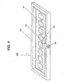
- FIG. 8 is a schematic diagram showing an exemplary pattern of the T branch circuit 150 of FIG. 4 as a dark area.
- the T branch circuit 150 comprises a root path 151, two branch paths 152, a stub 153 and step impedance transformers 154 and 155.
- the amplitude and the phase of the signals supplied to the antenna elements 122 are controlled by design parameters of the step impedance transformers 154 and 155.
- the T branch circuit 150 is configured symmetrical about the plane of symmetry that runs through the root path 151.
- the T branch circuit 150 is so configured. that each of the root path 151 and the branch paths 152 has a characteristic impedance of 50 ⁇ .
- the signal on the root path 151 is distributed into the two paths 152 with an equal power and a same phase.
- the branch paths 152 are coupled in serial with the antenna elements 122. Arrangements are made such that the overall impedance of the branch circuit has an impedance smaller than 50 ⁇ .
- the T branch circuit 150 achieves impedance matching by mainly using step impedance transformers (154 and 155x2) but using the fewest possible stubs (153). Doing this makes the band width of the whole circuit or array antenna 120 wider as compared with an ordinary circuit that uses stubs for impedance matching.
- an antenna has to have a frequency band width wider than the sum of the band width occupied by the communication system where the antenna is incorporated and a frequency error involved in the manufacturing process of the antenna.
- the inventive T branch circuit 150 enables implementation of such a wide band circuit or antenna.
- T branch circuit 150 having two branch paths.
- the invention is applicable to any T branch circuits having more than two branch paths.
- a wider band HF circuit and a communication system can be implemented by using a T branch circuit according to the principles of the invention.
- FIG. 9 is a diagram showing a reflection characteristic curve of the antenna 100 incorporating the inventive T branch circuit 140.
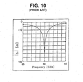
- FIG. 10 is a diagram showing a reflection characteristic curve of the conventional antenna 1 of FIG. 1.
- the axis of abscissas indicates the frequency from 35 through 45 GHz
- the axis of ordinates indicates the return loss viewed from the entrance to the root path.
- the T branch circuit 150 according to the invention have achieved matching such that the return loss is less than - 10 dB for 4 GHz from 37.3 through 42 GHz as shown in FIG. 9.
- the conventional T branch circuit 50 of FIG. 3 have achieved matching of less than -10 dB for 2 GHz from 39 through 41 GHz as shown in FIG. 10.
- a T branch circuit according to-the present invention yields substantially twice of the band width of conventional one.
Abstract
Description
- The present invention relates to a high frequency (HF) circuit in a communication device and more specifically to a technique for bonding a circuit board to a metal chassis or case, a waveguide-microstrip line transition, a branch circuit, and a high frequency circuit incorporating these elements.
- Recently, as frequency resources in communications technology are running dry, frequency bands available for building a new communications system have been and are shifting to higher bands. In this situation, the government and the people are jointly promoting a development to milliwave and microwave communication systems domestically and internationally. For example, it has been decided that extremely high frequency bands ranging from some GHz to hundreds GHz are assigned as available frequency bands to various communication systems under development for wireless LAN (local area network) and ITS (Intelligent Transport System).
- Since available frequencies are rising as described above, antennas and HF (high frequency) circuits are desired which satisfactorily work in milliwave and microwave bands. However, design and manufacturing techniques that have been believed to be available may not work satisfactorily with an increase in frequency. For this reason, there is a need for novel design and manufacturing techniques.
- FIG. 1 is a diagram showing an arrangement of a prior art
array antenna assembly 1. In FIG. 1, theantenna assembly 1 comprises andielectric substrate 10, acircuit pattern 20, achassis 30 that holds thedielectric substrate 10 and serves as the ground, and a waveguide-microstrip line transition 40. Thecircuit pattern 20, which constitutes an array antenna, includes aT branch circuit 50. A signal transmitted through a waveguide (not shown) is passed by thetransition 40 to a microstrip line of thecircuit pattern 20, and further passed by theT branch circuit 50 to the right and the left portions of the array antenna. - FIG. 2 is a schematic diagram showing an arrangement of the
transition 40 of FIG. 1. In FIG. 2, thetransition 40 comprises aridge waveguide 42, aridge 41 formed inside theridge waveguide 42, and amicrostrip line 21 which is formed on thedielectric substrate 10 and which is extending to (or a part of) thecircuit pattern 20. As described above, the signal transmitted through the not-shown waveguide is converted into a transmission mode of themicrostrip line 21 by theridge 41 provided inside thewaveguide 42 and transmitted to thearray antenna 20. - Problems exist in conjunction with working if an antenna with the just-described arrangements are to be implemented for milliwave or microwave. With an increase in frequency, dielectric materials available for the
dielectric layer 10 is limited to substances lack of a mechanical strength, e.g., ceramics, quartz, silicon, etc. Further, if an antenna that radiates a beam of two degrees in mesial width in a 76 GHz band is to be fabricated, thedielectric substrate 10 for the antenna will be approximately 100 to 300 µ m thick and 15 cm long in one side. Bonding such a thin andwide substrate 10 to thechassis 30 often results in a breakage of thedielectric substrate 10. Also, as the frequency increases, the characteristics of theantenna 20 depends strongly on the earthing state of thedielectric substrate 10. For this reason, a sufficient electrical contact is indispensable for the junction of thedielectric substrate 10 and thecircuit pattern 20. However, this is hard to be achieved by conventional techniques. - Since the degree of freedom is very low in designing a waveguide-microstrip line transition, i.e., the design parameters are limited only to the width, the length and the height of the
ridge 41, this sometimes causes the width of ridge for a milliwave band to be extremely narrow. Accordingly, the height of theridge 41 of thetransition 40, which is manufactured through machining of a brass material, becomes higher as compared with theridge 41 width, making the work difficult. The lack of the degree of freedom in design may disable the conversion into a microstrip line with a lower characteristic impedance and cause the problem that a too match difference between the widths of the designedridge 41 and themicrostrip line 21 leads to an unexpected deterioration in the line conversion characteristics. - As is not limited to a high frequency (HF) antenna, an
array antenna 20 as a whole generally exhibits a narrower frequency band characteristic with an increase in the number of array elements. Taking for example an antenna used in a front monitoring radar being put to practical use in 60 GHz, the antenna needs a beam width of about 2 degrees and accordingly a very large size. if a structure incorporating a conventional branch circuit were used as it is for such antenna, the resultant antenna would exhibit a very narrow frequency band characteristic, causing the band width of the antenna to be narrower than that of the radar. This is because conventional branch circuits mainly use stubs for impedance matching. FIG. 3 is a diagram showing an exemplary pattern of a conventional T branch circuit comprising a matching circuit that uses stubs 51 (the T branch circuit is shown as a dark area). Using stubs for impedance matching generally tends to narrow the frequency characteristics of the circuit. Specifically, the larger the distances (D1 and D2) between the matching circuit and circuits (22) that need matching, the narrower the frequency band of the whole circuit. However, if stubs are disposed too match near the antenna (or the circuits that need matching) to broaden the frequency band of the antenna, the antenna will fail to provide a desired characteristics. Thus, matching by stubs while providing a desired characteristic to the antenna or the circuits having their impedance matched inevitably narrows the frequency band of the resultant circuit such as an antenna. - The invention is directed to solving these and other problems and disadvantages of the prior art.
- It is an aim of the invention to provide a technique of bonding a thin and large-area circuit substrate to a metal layer with a sure and uniform contact but no fear of substrate breakage; a waveguide-microstrip transition that has a high degree of freedom in design and easy to work; and a branch circuit that permits the frequency band of circuit to be wide.
- It is another aim of the invention to provide a high frequency circuit and an antenna that incorporate an circuit substrate implemented by such a bonding technique, such a waveguide-microstrip transition and such a branch circuit, and to provide a communication system using such a high frequency circuit and such an antenna.
- According to an aspect of the invention, a method of bonding a circuit board with a metal plate is provided. The method includes the steps of working the metal plate so as to have a shape that permits a fluid to form a bath in an area including a part where the circuit board is to be bonded; heating the worked metal plate to such a temperature as melt a conductive bonding material; forming a bath of the conductive bonding material in the area of the metal plate; floating the circuit board on the bath; and absorbing excessive portion of the conductive material without applying a force to the dielectric substrate.
- A circuit assembly according to just-described aspect of the invention is provided with a thin and large-area dielectric substrate with an improved earthing condition. A bonding agent with a low melting point, a low melting point solder, etc. may be used as conductive material.
- According to another aspect of the invention, a branch circuit for branching a first path into at least two second paths in a high frequency circuit is provided.. The impedance matching between the first path and each of the branch paths is achieved by mainly using impedance transformers but by using fewest possible stub(s) in the branch circuit. The first path, the second paths, the impedance transformers, and the fewest possible stub(s) are arranged in symmetry with respect to a plane of symmetry that runs through the first path.
- In one embodiment, the impedance transformers are step impedance transformers.
- According to another aspect of the invention, a waveguide-microstrip line transition that is easy to work and low in transition loss is provided. The transition comprises a fanwise tube having a first opening coupled with a waveguide and a second opening larger in size then the first opening, a first and a second wider wall of the tube spreading from the first opening toward the second opening; an end portion of a microstrip line formed on a dielectric substrate arranged near the first wider wall, the end portion being situated a little inside the second opening and on a plane of symmetry for the first and the second wider walls; and a ridge formed on the second wider wall, the ridge protruding gradually from a first opening side toward a second opening side to become short-circuited, at the end thereof, with the end portion of the microstrip line, wherein dimensions of the fanwise tube and a shape of the first and the second wider walls are determined so as to fit the width of the microstrip line to the end portion of the microstrip line.
- In one embodiment, at least a part of each longitudinal side of a fanning-out portion of the wider walls is linear. However, at least a part of each longitudinal side may accords substantially with an exponential function or a trigonometric function.
- The features and advantages of the present invention will be apparent from the following description of an exemplary embodiment of the invention and the accompanying drawing, in which:
- FIG. 1 is a diagram showing an arrangement of a prior art
array antenna assembly 1; - FIG. 2 is a diagram showing an arrangement of the waveguide-
microstrip line transition 40 of FIG. 1; - FIG. 3 is a diagram showing an exemplary pattern of a conventional T branch circuit comprising a matching circuit that uses stubs;
- FIG, 4 is a schematic diagram showing an exemplary arrangement of an array antenna assembly according to an illustrative embodiment of the invention;
- FIG. 5 is a schematic sectional view taken along the plane X-Y of FIG. 4;
- FIG. 6 is a diagram showing an exemplary process of bonding the
metal layer 11 of a circuit board to thechassis 130 in accordance with the principles of the invention; - FIG. 7 is a schematic diagram showing an exemplary arrangement of
the waveguide-
microstrip line transition 140 of FIG. 4; - FIG. 8 is a schematic diagram showing an exemplary pattern of the
T branch circuit 150 of FIG. 4; - FIG. 9 is a diagram showing a reflection characteristic curve of the
antenna 100 incorporating the inventiveT branch circuit 140; and - FIG. 10 is a diagram showing a reflection characteristic curve of the
conventional antenna 1 of FIG. 1. -
- Throughout the drawing, the same elements when shown in more than one figure are designated by the same reference numerals.
- FIG. 4 is a schematic diagram showing an exemplary arrangement of an
array antenna assembly 100 according to an illustrative embodiment of the invention. In FIG. 4, theantenna assembly 100 comprises andielectric substrate 10, a circuit pattern or anarray antenna 120 formed by patterning a metal film on thedielectric substrate 10 through photocopying, etching, etc., achassis 130 that holds thedielectric substrate 10 and serves as the ground, and a waveguide-microstrip line transition 140 formed in the edge of thechassis 130. Thecircuit pattern 120 serves as a microstrip antenna array. A signal transmitted through a waveguide (not shown) is passed by thetransition 140 to a microstrip line coupled to thecircuit pattern 120, and further passed by theT branch circuit 50 to the right and the left portions of thearray antenna 120. - Bonding the Dielectric Substrate
- FIG. 5 is a schematic sectional view taken along the plane X-Y of FIG. 4. In FIG. 5, the
antenna assembly 100 comprisesmetal layers dielectric layer 10, asolder layer 111 and thechassis 130. Themetal layer 120 on thedielectric layer 10 comprises a circuit pattern forming a microstrip structure in cooperation with themetal layer 11. Themetal layer 120, thedielectric layer 10 and themetal layer 11 constitute acircuit board 120+10+11. According to the invention, themetal layer 11 of thecircuit board 120+10+11 is bonded with thechassis 130 by means of a bonding material of a good conductivity, which realizes sufficient earthing and strong support of the circuit board. In this specific embodiment, a lower-melting-point solder is used as the bonding material. It should be noted that thechassis 130 is not a flat plate but has a concavity on one side thereof as shown in FIG. 5. - FIG. 6 shows how the metal layer 11is bonded with the
chassis 130 in accordance with the principles of the invention. The processing steps are as follows: - (1) Put
solder 111a in the concavity of the heated chassis 130to make asolder bath 111b. Thesolder 111a is preferably a low melting point solder with a low melting point. Because if the difference between the rates of expansion for thesubstrate 10 and the chassis 130is large, heating too much for a higher melting point solder may cause thesubstrate 10 to break during a cooling process. - (2) Float the
circuit board 120+10+11 on thesolder bath 111b. The circuit. board floats of itself due to the surface tension of thesolder 111b. - (3) Get the
metal layer 11 of the circuit board attached to thesolder 111b, getting bubbles out from between the metal layer 11and thechassis 130. - (4) Remove excessive solder by absorbing
solder 111b little by little without applying external force directly to the circuit board. The absorption ofsolder 111b is achieved by using a dedicated copper fiber.. - (5) Cool taking a sufficient time such that any undesirable stress will not remain in the resultant assembly.
-
- The just-described process enables even a thin and large-area dielectric substrate 10 (i.e.,
circuit board 120+10+11) from which alone a sufficient mechanical strength can not be expected to be bonded with thechassis 130 without a fear of breaking the substrate 10 (or the circuit board), realizing good earthing. - Though the inventive bonding technique has been described in conjunction with an
antenna assembly 100 using anarray antenna pattern 20, the inventive technique may be applied to any high frequency (HF) circuit assembly with any circuit pattern. - It is noted that any suitable conductive bonding agents may be used instead of the
solder 111a. In this case, the bonding agents are preferably low in the temperature and small in the ratio of volume change at about the hardening temperature. - The inventive bonding technique has been described in conjunction with bonding a circuit board with a chassis. However, the inventive technique is applicable to bonding a thin and large-area circuit board with a metal surface in a concavity or a metal surface fringed with walls.
- Waveguide-Microstrip Line Transition FIG. 7 shows an exemplary arrangement of the waveguide-
microstrip line transition 140 of FIG. 4. In FIG. 7, thetransition 140 comprises anextension 42 of a waveguide (not shown), a fanwise tube (i.e., a tube spreading out toward the end) 142, aridge 144 so formed as to protrude inside thefanwise tube 142, and amicrostrip line 21 formed on thedielectric substrate 10 and extending to (or forming a part of) thecircuit pattern 120. Thefanwise tube 142 has a horn-like structure with a rectangular cross section perpendicular to the current direction. The two opening of thefanwise tube 142 differ in dimensions from each other. Thetransition 140 serves as a transition between thewaveguide extension 42 and themicrostrip line 121. Thetransition 140 is a so-called ridge waveguide converter provided, in the center of thefanwise tube 142, with aridge 144 of a wedge shape. Specifically, the electromagnetic fields distributed all over the opening of thewaveguide extension 42 is gradually converged on the head of theridge 144 and finally made resemble the electromagnetic transmission mode of themicrostrip line 121 thereby to be power-transmitted to themicrostrip line 121. - According to the present invention, the line conversion characteristics of the
transition 140 are a function of (i.e., can be controlled by) not only the dimensions of theridge 144 but also the shape of fanning of thefanwise tube 142. That is, using a tube spreading out like an unfolded fan has increased the degree of freedom in designing theridge 144. Since the designer can freely select the width and the height of theridge 144, thetransition 140 can be so designed as to have desired line conversion characteristics with a reduced parasitic impedance near the interface between theridge 144 head and themicrostrip line 121. In this way, theinventive transition 140 is easy to work, relatively lower in conversion loss and better in conversion characteristics. - Also, since the height of the
ridge 144 can be set identical to that of thefanwise tube 142, thefanwise tube 142 with a high precision in the dimensions is provided, which contributes to better line conversion characteristics of theresultant transition 140. - The
fanwise tube 142 has been shown as linearly shaped in FIG. 7. However, thetube 142 may have any nonlinear shape that spreads out toward the end. The side of thetube 142 may be curved according to, e.g., an exponential function, a trigonometric function, etc. The two opening of thetube 142 may have any suitable geometric shape different from each other to exhibit different characteristic impedance. - Though the
transition 140 has been described as a waveguide-microstrip transition provided in a path to an antenna, thetransition 140 according to the invention can be applied to an ordinary high frequency circuit. - Branch Circuit
- FIG. 8 is a schematic diagram showing an exemplary pattern of the
T branch circuit 150 of FIG. 4 as a dark area. In FIG. 8, theT branch circuit 150 comprises aroot path 151, twobranch paths 152, astub 153 andstep impedance transformers antenna elements 122 are controlled by design parameters of thestep impedance transformers T branch circuit 150 is configured symmetrical about the plane of symmetry that runs through theroot path 151. - In this specific embodiment, the
T branch circuit 150 is so configured. that each of theroot path 151 and thebranch paths 152 has a characteristic impedance of 50 Ω. The signal on theroot path 151 is distributed into the twopaths 152 with an equal power and a same phase. Thebranch paths 152 are coupled in serial with theantenna elements 122. Arrangements are made such that the overall impedance of the branch circuit has an impedance smaller than 50Ω. - It should be noted that the
T branch circuit 150 achieves impedance matching by mainly using step impedance transformers (154 and 155x2) but using the fewest possible stubs (153). Doing this makes the band width of the whole circuit orarray antenna 120 wider as compared with an ordinary circuit that uses stubs for impedance matching. Generally speaking, an antenna has to have a frequency band width wider than the sum of the band width occupied by the communication system where the antenna is incorporated and a frequency error involved in the manufacturing process of the antenna. The inventiveT branch circuit 150 enables implementation of such a wide band circuit or antenna. - An illustrative embodiment has been described in conjunction with the
T branch circuit 150 having two branch paths. However, the invention is applicable to any T branch circuits having more than two branch paths. A wider band HF circuit and a communication system can be implemented by using a T branch circuit according to the principles of the invention. - FIG. 9 is a diagram showing a reflection characteristic curve of the
antenna 100 incorporating the inventiveT branch circuit 140. FIG. 10 is a diagram showing a reflection characteristic curve of theconventional antenna 1 of FIG. 1. In FIGs. 9 and 10, the axis of abscissas indicates the frequency from 35 through 45 GHz, and the axis of ordinates indicates the return loss viewed from the entrance to the root path. TheT branch circuit 150 according to the invention have achieved matching such that the return loss is less than - 10 dB for 4 GHz from 37.3 through 42 GHz as shown in FIG. 9. On the other hand, the conventionalT branch circuit 50 of FIG. 3 have achieved matching of less than -10 dB for 2 GHz from 39 through 41 GHz as shown in FIG. 10. Thus, a T branch circuit according to-the present invention yields substantially twice of the band width of conventional one. - Many widely different embodiments of the present invention may be constructed without departing from the scope of the present invention. It should be understood that the present invention is not limited to the specific embodiments described in the specification, except as defined in the appended claims.
Claims (4)
- A waveguide-microstrip line transition that is easy to work and low in transition loss, comprising:a fanwise tube having a first opening coupled with a waveguide and a second opening larger in size than said first opening, a first and a second wider wall of said tube spreading from said first opening toward said second opening;an end portion of a microstrip line formed on a dielectric substrate arranged near said first wider wall, said end portion being situated a little inside said second opening and on a plane of symmetry for said first and said second wider walls; anda ridge formed on said second wider wall, said ridge protruding gradually from a first opening side toward a second opening side to become short-circuited, at the end thereof, with said end portion of said microstrip line, wherein dimensions of said fanwise tube and a shape of said first and said second wider walls are determined so as to fit the width of said microstrip line to said end portion of said microstrip line.
- A waveguide-microstrip line transition as defined in claim 1, wherein at least a part of each longitudinal side of fanning-out portion of said wider walls is substantially linear.
- A waveguide-microstrip line transition as defined in claim 1 or 2, wherein at least a part of each longitudinal side of a fanning-out portion of said wider walls accords substantially with an exponential function.
- A waveguide-microstrip line transition as defined in claim 1, 2 or 3, wherein at least a part of each longitudinal side of a fanning-out portion of said wider walls accords substantially with a trigonometric function.
Applications Claiming Priority (3)
| Application Number | Priority Date | Filing Date | Title |
|---|---|---|---|
| JP11831898 | 1998-04-28 | ||
| JP10118318A JPH11312881A (en) | 1998-04-28 | 1998-04-28 | Substrate welding method, and high-frequency circuit, antenna, waveguide, line converter, line branching circuit and communication system |
| EP99303201A EP0954049B1 (en) | 1998-04-28 | 1999-04-26 | Circuit board bonding method |
Related Parent Applications (1)
| Application Number | Title | Priority Date | Filing Date |
|---|---|---|---|
| EP99303201A Division EP0954049B1 (en) | 1998-04-28 | 1999-04-26 | Circuit board bonding method |
Publications (2)
| Publication Number | Publication Date |
|---|---|
| EP1321998A1 true EP1321998A1 (en) | 2003-06-25 |
| EP1321998B1 EP1321998B1 (en) | 2004-10-13 |
Family
ID=14733712
Family Applications (3)
| Application Number | Title | Priority Date | Filing Date |
|---|---|---|---|
| EP04024636A Withdrawn EP1496563A3 (en) | 1998-04-28 | 1999-04-26 | Circuit board bonded to ground, "T" branching circuit, waveguide-microstrip transition |
| EP03006544A Expired - Lifetime EP1321998B1 (en) | 1998-04-28 | 1999-04-26 | Waveguide-microstrip transition for millimeter waves and Microwaves |
| EP99303201A Expired - Lifetime EP0954049B1 (en) | 1998-04-28 | 1999-04-26 | Circuit board bonding method |
Family Applications Before (1)
| Application Number | Title | Priority Date | Filing Date |
|---|---|---|---|
| EP04024636A Withdrawn EP1496563A3 (en) | 1998-04-28 | 1999-04-26 | Circuit board bonded to ground, "T" branching circuit, waveguide-microstrip transition |
Family Applications After (1)
| Application Number | Title | Priority Date | Filing Date |
|---|---|---|---|
| EP99303201A Expired - Lifetime EP0954049B1 (en) | 1998-04-28 | 1999-04-26 | Circuit board bonding method |
Country Status (4)
| Country | Link |
|---|---|
| US (2) | US6335664B1 (en) |
| EP (3) | EP1496563A3 (en) |
| JP (1) | JPH11312881A (en) |
| DE (2) | DE69925880T2 (en) |
Cited By (1)
| Publication number | Priority date | Publication date | Assignee | Title |
|---|---|---|---|---|
| CN105680136A (en) * | 2016-03-21 | 2016-06-15 | 南京邮电大学 | Transition circuit from coplanar waveguide to groove line and to substrate integrated non-radiation dielectric waveguides |
Families Citing this family (26)
| Publication number | Priority date | Publication date | Assignee | Title |
|---|---|---|---|---|
| US6466176B1 (en) * | 2000-07-11 | 2002-10-15 | In4Tel Ltd. | Internal antennas for mobile communication devices |
| SE519904C2 (en) | 2000-12-29 | 2003-04-22 | Amc Centurion Ab | Manufacture of antenna devices |
| US6693557B2 (en) | 2001-09-27 | 2004-02-17 | Wavetronix Llc | Vehicular traffic sensor |
| TW517613U (en) * | 2001-11-13 | 2003-01-11 | Asustek Comp Inc | Jig framework featuring with solder attracting function |
| WO2005067357A1 (en) * | 2003-12-24 | 2005-07-21 | Molex Incorporated | Transmission line with a transforming impedance and solder lands |
| JP2006287452A (en) * | 2005-03-31 | 2006-10-19 | Digital Electronics Corp | Antenna device and electronic apparatus |
| US7606592B2 (en) * | 2005-09-19 | 2009-10-20 | Becker Charles D | Waveguide-based wireless distribution system and method of operation |
| US8248272B2 (en) | 2005-10-31 | 2012-08-21 | Wavetronix | Detecting targets in roadway intersections |
| US8665113B2 (en) | 2005-10-31 | 2014-03-04 | Wavetronix Llc | Detecting roadway targets across beams including filtering computed positions |
| US20070178766A1 (en) * | 2006-01-31 | 2007-08-02 | Intel Corporation | Passive impedance equalization of high speed serial links |
| US7420436B2 (en) * | 2006-03-14 | 2008-09-02 | Northrop Grumman Corporation | Transmission line to waveguide transition having a widened transmission with a window at the widened end |
| KR100846515B1 (en) * | 2007-03-19 | 2008-07-17 | 삼성전자주식회사 | 90° bent metallic waveguide having tapered c-shaped aperture, method of fabricating the same, light delivery module employing the waveguide and heat assisted magnetic recording head employing the bending waveguide |
| CN102386480A (en) * | 2010-08-27 | 2012-03-21 | 上海任虹精密机械有限公司 | Production method and system of soft-board antenna |
| CN102157769B (en) * | 2011-03-25 | 2013-11-06 | 东南大学 | Microstrip line-slot line transition structure with stop band |
| US9412271B2 (en) | 2013-01-30 | 2016-08-09 | Wavetronix Llc | Traffic flow through an intersection by reducing platoon interference |
| JP6094379B2 (en) * | 2013-05-22 | 2017-03-15 | 富士通株式会社 | Waveguide-microstrip line converter |
| CN103464337B (en) * | 2013-08-13 | 2016-02-24 | 昆山龙腾光电有限公司 | Point glue solidify device |
| FR3010835B1 (en) * | 2013-09-19 | 2015-09-11 | Inst Mines Telecom Telecom Bretagne | JUNCTION DEVICE BETWEEN A PRINTED TRANSMISSION LINE AND A DIELECTRIC WAVEGUIDE |
| JP6250468B2 (en) * | 2014-04-23 | 2017-12-20 | 日本ピラー工業株式会社 | Planar antenna |
| KR20240005985A (en) * | 2017-01-18 | 2024-01-12 | 피닉스 엘엘씨 | High power ion beam generator systems and methods |
| CN106956055B (en) * | 2017-05-08 | 2023-06-23 | 成都锦江电子系统工程有限公司 | High-efficient high quality radar oscillator shell welding jig |
| JP6896109B2 (en) * | 2018-01-10 | 2021-06-30 | 三菱電機株式会社 | Waveguide microstrip line converters and antenna devices |
| CN109888511B (en) * | 2019-04-15 | 2023-12-08 | 上海几何伙伴智能驾驶有限公司 | Circularly polarized microstrip panel antenna |
| CN112670690B (en) * | 2020-11-10 | 2022-01-11 | 北京遥测技术研究所 | High-temperature ceramic transition circuit based on resonant mode |
| CN113328227A (en) * | 2021-05-27 | 2021-08-31 | 电子科技大学 | Transition structure from microstrip line to non-radiative dielectric waveguide |
| CN113460689B (en) * | 2021-06-29 | 2023-05-23 | 东方日升(常州)新能源有限公司 | Method for transferring silicon wafer |
Citations (2)
| Publication number | Priority date | Publication date | Assignee | Title |
|---|---|---|---|---|
| GB763894A (en) * | 1954-01-14 | 1956-12-19 | Standard Telephones Cables Ltd | Radio frequency transmission system |
| US3579149A (en) * | 1969-12-08 | 1971-05-18 | Westinghouse Electric Corp | Waveguide to stripline transition means |
Family Cites Families (11)
| Publication number | Priority date | Publication date | Assignee | Title |
|---|---|---|---|---|
| US3815055A (en) * | 1973-04-20 | 1974-06-04 | Raytheon Co | Microwave power divider |
| US3969691A (en) * | 1975-06-11 | 1976-07-13 | The United States Of America As Represented By The Secretary Of The Navy | Millimeter waveguide to microstrip transition |
| US4226659A (en) * | 1976-12-27 | 1980-10-07 | Bell Telephone Laboratories, Incorporated | Method for bonding flexible printed circuitry to rigid support plane |
| US4168479A (en) * | 1977-10-25 | 1979-09-18 | The United States Of America As Represented By The Secretary Of The Navy | Millimeter wave MIC diplexer |
| CA1290676C (en) * | 1987-03-30 | 1991-10-15 | William Frank Graham | Method for bonding integrated circuit chips |
| JPH04348540A (en) * | 1991-05-27 | 1992-12-03 | Sony Corp | Flip chip bonder |
| US5210941A (en) * | 1991-07-19 | 1993-05-18 | Poly Circuits, Inc. | Method for making circuit board having a metal support |
| JPH05283915A (en) | 1992-03-31 | 1993-10-29 | Toshiba Corp | Waveguide-microstrip line converter |
| JPH05335816A (en) | 1992-06-03 | 1993-12-17 | Japan Radio Co Ltd | Waveguide-microstrip line converter |
| US5906310A (en) * | 1994-11-10 | 1999-05-25 | Vlt Corporation | Packaging electrical circuits |
| JP3476351B2 (en) * | 1997-11-27 | 2003-12-10 | シャープ株式会社 | Low noise amplifier |
-
1998
- 1998-04-28 JP JP10118318A patent/JPH11312881A/en active Pending
-
1999
- 1999-04-13 US US09/290,395 patent/US6335664B1/en not_active Expired - Fee Related
- 1999-04-26 EP EP04024636A patent/EP1496563A3/en not_active Withdrawn
- 1999-04-26 EP EP03006544A patent/EP1321998B1/en not_active Expired - Lifetime
- 1999-04-26 EP EP99303201A patent/EP0954049B1/en not_active Expired - Lifetime
- 1999-04-26 DE DE69925880T patent/DE69925880T2/en not_active Expired - Fee Related
- 1999-04-26 DE DE69921204T patent/DE69921204T2/en not_active Expired - Fee Related
-
2001
- 2001-11-15 US US09/987,625 patent/US6592021B2/en not_active Expired - Fee Related
Patent Citations (2)
| Publication number | Priority date | Publication date | Assignee | Title |
|---|---|---|---|---|
| GB763894A (en) * | 1954-01-14 | 1956-12-19 | Standard Telephones Cables Ltd | Radio frequency transmission system |
| US3579149A (en) * | 1969-12-08 | 1971-05-18 | Westinghouse Electric Corp | Waveguide to stripline transition means |
Non-Patent Citations (1)
| Title |
|---|
| ZARBA G ET AL: "AN OPTIMISED WAVEGUIDE TO MICROSTRIP TRANSITION AT K BAND", PROCEEDINGS OF THE 26TH. EUROPEAN MICROWAVE CONFERENCE 1996. PRAGUE, SEPT. 9 - 13, 1996, PROCEEDINGS OF THE EUROPEAN MICROWAVE CONFERENCE, SWANLEY, NEXUS MEDIA, GB, vol. 2 CONF. 26, 9 September 1996 (1996-09-09), pages 836 - 838, XP000682646, ISBN: 1-899919-08-2 * |
Cited By (1)
| Publication number | Priority date | Publication date | Assignee | Title |
|---|---|---|---|---|
| CN105680136A (en) * | 2016-03-21 | 2016-06-15 | 南京邮电大学 | Transition circuit from coplanar waveguide to groove line and to substrate integrated non-radiation dielectric waveguides |
Also Published As
| Publication number | Publication date |
|---|---|
| EP0954049A3 (en) | 2002-07-24 |
| DE69925880D1 (en) | 2005-07-28 |
| US6335664B1 (en) | 2002-01-01 |
| DE69921204T2 (en) | 2005-11-10 |
| EP1321998B1 (en) | 2004-10-13 |
| DE69921204D1 (en) | 2004-11-18 |
| EP1496563A3 (en) | 2005-04-13 |
| US20020047038A1 (en) | 2002-04-25 |
| DE69925880T2 (en) | 2006-05-11 |
| EP0954049A2 (en) | 1999-11-03 |
| EP1496563A2 (en) | 2005-01-12 |
| US6592021B2 (en) | 2003-07-15 |
| JPH11312881A (en) | 1999-11-09 |
| EP0954049B1 (en) | 2005-06-22 |
Similar Documents
| Publication | Publication Date | Title |
|---|---|---|
| US6592021B2 (en) | Circuit board bonding method, branch circuit and its designing method, waveguide-microstrip transition, and application to HF circuit, antenna and communication system | |
| Grabherr et al. | Microstrip to waveguide transition compatible with mm-wave integrated circuits | |
| US7561006B2 (en) | Low loss electrical delay line | |
| JP3241139B2 (en) | Film carrier signal transmission line | |
| US2825876A (en) | Radio frequency transducers | |
| KR101718761B1 (en) | Millimeter Wave Antenna for Diagonal Radiation | |
| CN108777343B (en) | Substrate integrated waveguide transmission structure, antenna structure and connection method | |
| GB2316233A (en) | Wide band radiating device capable of several polarizations | |
| JP2005051331A (en) | Coupling structure between microstrip line and dielectric waveguide | |
| CN115568094A (en) | Switch based on substrate integrated fin line structure | |
| Simons et al. | New techniques for exciting linearly tapered slot antennas with coplanar waveguide | |
| GB2222489A (en) | Waveguide apparatus | |
| CN209571548U (en) | A kind of microstrip type ISGW circular polarisation gap travelling-wave aerial | |
| US6888429B2 (en) | Transmission line with a projecting dielectric part having an opposing coplanar line and transceiver | |
| Vasanelli et al. | A 77-GHz cavity antenna array in PCB technology | |
| WO2022042318A1 (en) | Spoof surface plasmon polariton transmission line structure, circuit board and electronic device | |
| JP3310643B2 (en) | Power distribution circuit | |
| US7224239B2 (en) | Structural element having a coplanar line | |
| Kinayman et al. | A novel surface-mountable millimeter-wave bandpass filter | |
| US11069949B2 (en) | Hollow-waveguide-to-planar-waveguide transition circuit comprising a coupling conductor disposed over slots in a ground conductor | |
| CN109950688A (en) | Microstrip type ISGW circular polarisation gap travelling-wave aerial | |
| JP2000174515A (en) | Coplanar waveguide - waveguide converter | |
| JPH10313203A (en) | High frequency transmission line | |
| CN110931967B (en) | K-band antenna, K-band array antenna and preparation method | |
| KR20010112034A (en) | Power combining structure using waveguide-to-microstrip transition |
Legal Events
| Date | Code | Title | Description |
|---|---|---|---|
| PUAI | Public reference made under article 153(3) epc to a published international application that has entered the european phase |
Free format text: ORIGINAL CODE: 0009012 |
|
| AC | Divisional application: reference to earlier application |
Ref document number: 0954049 Country of ref document: EP Kind code of ref document: P |
|
| AK | Designated contracting states |
Designated state(s): AT BE CH CY DE DK ES FI FR GB GR IE IT LI LU MC NL PT SE |
|
| AX | Request for extension of the european patent |
Extension state: AL LT LV MK RO SI |
|
| 17P | Request for examination filed |
Effective date: 20030811 |
|
| 17Q | First examination report despatched |
Effective date: 20030908 |
|
| GRAP | Despatch of communication of intention to grant a patent |
Free format text: ORIGINAL CODE: EPIDOSNIGR1 |
|
| AKX | Designation fees paid |
Designated state(s): DE GB |
|
| RTI1 | Title (correction) |
Free format text: WAVEGUIDE-MICROSTRIP TRANSITION FOR MILLIMETER WAVES AND MICROWAVES |
|
| GRAS | Grant fee paid |
Free format text: ORIGINAL CODE: EPIDOSNIGR3 |
|
| GRAA | (expected) grant |
Free format text: ORIGINAL CODE: 0009210 |
|
| AC | Divisional application: reference to earlier application |
Ref document number: 0954049 Country of ref document: EP Kind code of ref document: P |
|
| AK | Designated contracting states |
Kind code of ref document: B1 Designated state(s): DE GB |
|
| REG | Reference to a national code |
Ref country code: GB Ref legal event code: FG4D |
|
| REF | Corresponds to: |
Ref document number: 69921204 Country of ref document: DE Date of ref document: 20041118 Kind code of ref document: P |
|
| PLBE | No opposition filed within time limit |
Free format text: ORIGINAL CODE: 0009261 |
|
| STAA | Information on the status of an ep patent application or granted ep patent |
Free format text: STATUS: NO OPPOSITION FILED WITHIN TIME LIMIT |
|
| 26N | No opposition filed |
Effective date: 20050714 |
|
| PGFP | Annual fee paid to national office [announced via postgrant information from national office to epo] |
Ref country code: DE Payment date: 20070419 Year of fee payment: 9 |
|
| PGFP | Annual fee paid to national office [announced via postgrant information from national office to epo] |
Ref country code: GB Payment date: 20070425 Year of fee payment: 9 |
|
| GBPC | Gb: european patent ceased through non-payment of renewal fee |
Effective date: 20080426 |
|
| PG25 | Lapsed in a contracting state [announced via postgrant information from national office to epo] |
Ref country code: DE Free format text: LAPSE BECAUSE OF NON-PAYMENT OF DUE FEES Effective date: 20081101 |
|
| PG25 | Lapsed in a contracting state [announced via postgrant information from national office to epo] |
Ref country code: GB Free format text: LAPSE BECAUSE OF NON-PAYMENT OF DUE FEES Effective date: 20080426 |