EP1321790A2 - Optical package substrate and optical device - Google Patents
Optical package substrate and optical device Download PDFInfo
- Publication number
- EP1321790A2 EP1321790A2 EP02026653A EP02026653A EP1321790A2 EP 1321790 A2 EP1321790 A2 EP 1321790A2 EP 02026653 A EP02026653 A EP 02026653A EP 02026653 A EP02026653 A EP 02026653A EP 1321790 A2 EP1321790 A2 EP 1321790A2
- Authority
- EP
- European Patent Office
- Prior art keywords
- optical
- package substrate
- substrate
- section
- optical package
- Prior art date
- Legal status (The legal status is an assumption and is not a legal conclusion. Google has not performed a legal analysis and makes no representation as to the accuracy of the status listed.)
- Withdrawn
Links
Images




Classifications
-
- G—PHYSICS
- G02—OPTICS
- G02B—OPTICAL ELEMENTS, SYSTEMS OR APPARATUS
- G02B6/00—Light guides; Structural details of arrangements comprising light guides and other optical elements, e.g. couplings
- G02B6/10—Light guides; Structural details of arrangements comprising light guides and other optical elements, e.g. couplings of the optical waveguide type
- G02B6/12—Light guides; Structural details of arrangements comprising light guides and other optical elements, e.g. couplings of the optical waveguide type of the integrated circuit kind
-
- G—PHYSICS
- G02—OPTICS
- G02B—OPTICAL ELEMENTS, SYSTEMS OR APPARATUS
- G02B6/00—Light guides; Structural details of arrangements comprising light guides and other optical elements, e.g. couplings
- G02B6/24—Coupling light guides
- G02B6/42—Coupling light guides with opto-electronic elements
- G02B6/4201—Packages, e.g. shape, construction, internal or external details
- G02B6/4204—Packages, e.g. shape, construction, internal or external details the coupling comprising intermediate optical elements, e.g. lenses, holograms
- G02B6/4214—Packages, e.g. shape, construction, internal or external details the coupling comprising intermediate optical elements, e.g. lenses, holograms the intermediate optical element having redirecting reflective means, e.g. mirrors, prisms for deflecting the radiation from horizontal to down- or upward direction toward a device
-
- G—PHYSICS
- G02—OPTICS
- G02B—OPTICAL ELEMENTS, SYSTEMS OR APPARATUS
- G02B6/00—Light guides; Structural details of arrangements comprising light guides and other optical elements, e.g. couplings
- G02B6/24—Coupling light guides
- G02B6/42—Coupling light guides with opto-electronic elements
-
- G—PHYSICS
- G02—OPTICS
- G02B—OPTICAL ELEMENTS, SYSTEMS OR APPARATUS
- G02B6/00—Light guides; Structural details of arrangements comprising light guides and other optical elements, e.g. couplings
- G02B6/24—Coupling light guides
- G02B6/42—Coupling light guides with opto-electronic elements
- G02B6/4201—Packages, e.g. shape, construction, internal or external details
- G02B6/4219—Mechanical fixtures for holding or positioning the elements relative to each other in the couplings; Alignment methods for the elements, e.g. measuring or observing methods especially used therefor
- G02B6/4228—Passive alignment, i.e. without a detection of the degree of coupling or the position of the elements
- G02B6/423—Passive alignment, i.e. without a detection of the degree of coupling or the position of the elements using guiding surfaces for the alignment
Definitions
- the present invention relates to an optical package substrate and an optical device, and more particularly to a package substrate having a surface configuration suitable for mounting optical components and/or optical elements thereon, and a molding method for such a package substrate; and an optical device constructed by employing the package substrate.
- Optical communication systems employing optical fibers are evolving themselves from conventional long haul communication systems into subscriber communication systems. Subscriber-type optical communication systems require the use of small and inexpensive optical devices.
- optical components such as optical fibers and/or lenses and optical elements such as lasers and/or photodiodes are deployed in a coaxial arrangement.
- the positioning of optical fibers and lenses requires a high precision, e.g., a tolerance of ⁇ 1 ⁇ m. Therefore, a so-called active alignment technique has been used for the assembly of an optical device, where the positioning of the components is adjusted while driving the optical elements with laser light actually being led therethrough.
- this technique requires complicated tasks, and is time-consuming, thus presenting a substantial cost problem.
- FIG. 19 is a cross-sectional view showing an exemplary optical device structure which utilizes a conventionally-proposed deflection method.
- an end face of an optical fiber (or an optical waveguide) 191 is ground at 45° , with a reflection mirror 192 being provided on this end face.
- Light guided through the optical fiber (optical waveguide) 191 which is incident from the left direction in FIG. 19 has its optical path turned (i.e., deflected) by 90° at the mirror 192, so as to be received by the photodiode 193.
- the photodiode 193 may be of a surface reception type as that shown in FIG. 19, or of a different type called a "waveguide type".
- a surface reception type photodiode has a large area for receiving light, so that it only requires a positioning precision of only about ⁇ tens of microns ( ⁇ m) with respect to an optical fiber or an optical waveguide. Therefore, the mounting of a surface reception type photodiode can be realized through a passive alignment, which involves forming markers on the substrate as reference points for the mounting process.
- a passive alignment which involves forming markers on the substrate as reference points for the mounting process.
- An example of this situation is monitoring of a laser output, where surface reception type photodiodes are a common choice.
- a waveguide type photodiode has a light receiving layer on the order of several microns. Therefore, a positioning precision as stringent as ⁇ 1 ⁇ m is required in order to ensure that light guided through an optical fiber or optical waveguide is properly coupled to a waveguide type photodiode.
- active alignment is usually employed for waveguide type photodiodes, thereby presenting a substantial mounting cost problem.
- FIG 20 shows another exemplary optical device structure utilizing the conventional deflection method described in Japanese Patent Laid-Open Publication No. 11-326662.
- this optical device features a reflective member 201, which is formed by processing a portion of an optical waveguide into a reflective surface for reflecting light.
- Light which is propagated through the waveguide layer 202 to exit at its end face is deflected by 90° , so as to be received by a surface reception type photodiode 203.
- conventional optical device structures are based on the concept of deflecting an optical path of light exiting from an optical fiber or optical waveguide so as to allow the exiting light to be received by a surface reception type photodiode, which requires a relatively low receiving positioning precision, with a view to reducing the device cost.
- the conventional optical device structures illustrated in FIGS. 19 and 20 require an additional process of working an end face of an optical fiber (or an optical waveguide) into a face having a 45° slope.
- it is essential to secure a high planar precision, so that processes such as grinding, dry etching, wet etching, and cutting must be carried out with a good reproducibility.
- an optical fiber processed so as to have a slanting end face is employed, light exiting from the optical fiber may not be properly incident on a photodiode if the optical fiber fails to be mounted in the correct orientation, due to rotation or the like.
- the objectives of the present invention are to provide an easy-to-manufacture optical package substrate which allows for easy mounting of optical elements such as photodiodes and lasers, and which is excellent in functionality, producibility, and economy, and a molding method for such an optical package substrate; and to provide an optical device constructed by employing the package substrate.
- the present invention has the following features to attain the above object.
- a first aspect of the present invention is directed to an optical package substrate for mounting an optical component and/or an optical element thereon, comprising: a guide section for fixing an optical axis of an optical fiber mounted in the guide section, the guide section being a groove formed on a surface of a substrate and extending from an end face of the substrate to a predetermined portion of the substrate; and an optical path deflection section for deflecting an optical path by reflection, the optical path deflection section being formed at the predetermined portion of the guide section so as to be in a position intersecting the optical axis of the optical fiber mounted in the guide section.
- a guide section used for the positioning of an optical fiber, and an optical path deflection section for deflecting light through reflection are concurrently molded onto an optical package substrate.
- a second aspect according to the present invention is directed to an optical package substrate for mounting an optical component and/or an optical element thereon, comprising: a waveguide section as a groove formed on a surface of a substrate and extending from an end face of the substrate to a predetermined portion of the substrate, the waveguide section corresponding to a predetermined optical waveguide core pattern; and an optical path deflection section for deflecting an optical path by reflection, the optical path deflection section being formed at the predetermined portion of the waveguide section so as to be in a position intersecting an optical axis of the optical waveguide defined in the waveguide section.
- a waveguide section corresponding to an optical waveguide core pattern and an optical path deflection section for deflecting light through reflection are concurrently molded onto an optical package substrate.
- a third aspect according to the present invention is directed to an optical package substrate for mounting an optical component and/or an optical element thereon, comprising: a stage portion for fixing an optical axis of a light receiving/emitting element mounted on the stage portion, the stage portion being formed on a surface of a substrate; and an optical path deflection section for deflecting an optical path by reflection, the optical path deflection section being formed on the surface of the substrate so as to be in a position intersecting the optical axis of the light receiving/emitting element mounted on the stage portion.
- a stage portion, used for the positioning of a light receiving/emitting element and an optical path deflection section for deflecting light through reflection are concurrently molded onto an optical package substrate.
- a waveguide section is further comprised which is formed on the surface of the substrate, the waveguide section corresponding to an optical waveguide core pattern having an optical axis coinciding with an optical axis of the light receiving/emitting element mounted on the stage portion.
- a waveguide section corresponding to an optical waveguide core pattern, a stage portion, and an optical path deflection section are concurrently molded onto an optical package substrate.
- a thin film element having a mirror property is provided on the optical path deflection section.
- a thin film element having a mirror property is provided on the optical path deflection section.
- a diffraction grating for creating different optical paths for different optical wavelengths is provided on the optical path deflection section.
- an optical device comprising a filtering function for receiving light of only a specific wavelength can be realized.
- the optical path deflection section has a curvature for converging a plurality of incident rays through reflection.
- the positioning precision for a light receiving element can be further relaxed, or light emitted from a surface emission type light emitting element can be converged so as to be coupled to an optical fiber or an optical waveguide with a high efficiency.
- the optical package substrate preferably comprises glass.
- glass By employing glass, it becomes possible to form highly precise configuration on a surface by means of a die, and excellent stability can be provided in various environments. Since glass is transmissive to UV rays, the fixing of an optical fiber or the like can be achieved by using a UV-curing adhesive, instead of a time-consuming thermosetting adhesive.
- the optical package substrate may be molded by pressing a die against a substrate material softened by being heated to a high temperature to transcribe an inverted pattern of the die onto the substrate material, the die having been obtained by using a normal-grinding tool and an arbitrary fine-grinding tool, wherein at least one of the die and the fine-grinding tool is obtained through microdischarge machining.
- the optical package substrate according to the present invention can be obtained.
- a fifth aspect according to the present invention is directed to an optical device having an optical component and/or optical element mounted on an optical package substrate, the optical package substrate comprising: a guide section for fixing an optical axis of an optical fiber mounted in the guide section, the guide section being a groove formed on a surface of a substrate and extending from an end face of the substrate to a predetermined portion of the substrate; and an optical path deflection section for deflecting an optical path by reflection, the optical path deflection section being formed at the predetermined portion of the guide section so as to be in a position intersecting the optical axis of the optical fiber mounted in the guide section, wherein the optical fiber placed in the guide section on the optical package substrate is pressed from above by a predetermined substrate, whereby the optical fiber is affixed to the optical package substrate.
- an optical fiber can be firmly mounted on an optical package substrate, and an optical device capable of deflecting light propagated through an optical fiber can be produced from the optical package substrate through very simple steps, leading to excellent productivity and economy. It is also possible to employ a predetermined substrate as a stage on which to mount a photodiode, a laser, or the like.
- a sixth aspect according to the present invention is directed to an optical device having an optical component and/or optical element mounted on an optical package substrate, the optical package substrate comprising: a waveguide section as a groove formed on a surface of a substrate and extending from an end face of the substrate to a predetermined portion of the substrate, the waveguide section corresponding to a predetermined optical waveguide core pattern; and an optical path deflection section for deflecting an optical path by reflection, the optical path deflection section being formed at the predetermined portion of the waveguide section so as to be in a position intersecting an optical axis of the optical waveguide defined in the waveguide section, the optical device further comprising a predetermined substrate, wherein a core material having a refractive index higher than a refractive index of the optical package substrate is filled in the waveguide section of the optical package substrate, and thereafter an adhesive having a refractive index lower than the refractive index of the core material is used to attach the predetermined substrate to the waveguide section.
- an optical device capable of deflecting light propagated through an optical fiber can be produced from the optical package substrate through very simple steps, leading to excellent productivity and economy.
- a seventh aspect according to the present invention is directed to an optical device having an optical component and/or optical element mounted on an optical package substrate, the optical package substrate comprising: a stage portion for fixing an optical axis of a light receiving/emitting element mounted on the stage portion, the stage portion being formed on a surface of a substrate; and an optical path deflection section for deflecting an optical path by reflection, the optical path deflection section being formed on the surface of the substrate so as to be in a position intersecting the optical axis of the light receiving/emitting element mounted on the stage portion wherein the light receiving/emitting element is affixed to the stage portion on the optical package substrate.
- an optical device capable of realizing optical coupling between a light receiving/emitting element and another optical element can be produced from an optical package substrate through very simple steps, by simply affixing a light receiving/emitting element on a stage portion through passive alignment.
- excellent productivity and economy can be obtained.
- the optical package substrate further comprises a waveguide section formed on the surface of the substrate, the waveguide section corresponding to an optical waveguide core pattern having an optical axis coinciding with an optical axis of the light receiving/emitting element mounted on the stage portion, the optical device further comprising a predetermined substrate, wherein a core material having a refractive index higher than a refractive index of the optical package substrate is filled in the waveguide section of the optical package substrate, and thereafter an adhesive having a refractive index lower than the refractive index of the core material is used to attach the predetermined substrate to the waveguide section.
- an optical device capable of realizing optical coupling between a light receiving/emitting element and another optical element can be produced from an optical package substrate through very simple steps, by simply affixing a light receiving/emitting element on a stage portion through passive alignment.
- excellent productivity and economy can be obtained.
- the optical device may further comprise a surface mounting type light receiving/emitting element which is optically coupled to the optical fiber affixed in the guide section through the optical path deflected by the optical path deflection section.
- the optical device may further comprise a surface mounting type light receiving/emitting element which is optically coupled to the optical waveguide defined in the waveguide section through the optical path deflected by the optical path deflection section.
- the optical device may further comprise a surface mounting type light receiving/emitting element which is optically coupled to the light receiving/emitting element affixed to the stage portion through the optical path deflected by the optical path deflection section.
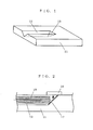
- FIG. 1 is a perspective view illustrating the configuration of an optical package substrate 11 according to a first embodiment of the present invention.
- a guide groove 12 for positioning an optical fiber is formed on the surface of the optical package substrate 11, with a tapered face 13 being formed adjoining the guide groove 12.
- the tapered face 13 constitutes a predetermined angle with respect to the surface of the optical package substrate 11.
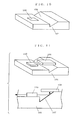
- FIG. 2 is a cross-sectional view illustrating an optical device incorporating the optical package substrate 11 of FIG. 1, with an optical fiber 15 and a surface reception type photodiode 16 being mounted thereon.
- the optical device structure incorporating the optical package substrate 11 includes a mirror 17 composed of a thin film capable of reflecting light, which is formed on the tapered face 13.
- the optical fiber 15 is affixed in the guide groove 12 by using an ultraviolet (UV) -curing resin, for example.
- the optical fiber 15 only needs to be placed within the guide groove 12, but is preferably placed in such a manner that an end face thereof abuts against the tapered face 13, as shown in FIG. 2.
- Above the tapered face 13 is mounted the surface reception type photodiode 16, which is placed in a position for receiving light deflected by the mirror 17 provided on the tapered face 13.
- the optical device shown in FIG. 2 incorporating the optical package substrate 11 functions as a light receiving module.
- the optical package substrate 11 As described above, by employing the optical package substrate 11 according to the first embodiment of the present invention, it is possible to produce an optical device capable of easily deflecting the light which exits the optical fiber 15. Moreover, there is no need to watch the rotation of the optical fiber 15 during the mounting of a component.
- the mirror 17 on the tapered face 13 may be formed by directly applying a metal film through a plating or vacuum process.
- a mirror which is previously formed on another substrate may be attached by adhering the substrate onto the tapered face 13.
- a multilayer film filter which reflects light of a target optical wavelength may be formed on the tapered face 13.
- the aforementioned angle of the tapered face 13 is preferably in the range of about 30° to about 70° .
- the angle is about 60° or more as to minimize any fluctuations in characteristics associated with polarization.
- the cross section of the guide groove 12 is not limited to a V shape. Rather, any cross sectional shape may be used which permits the optical fiber 15 to be positioned therein, e.g., rectangular, semicircular, or like shapes.
- an optical fiber 191 shown in FIG. 19 may be employed, which is provided with a mirror that is ground at a predetermined angle on one end face; in this case, it is unnecessary to form the mirror 17 on the tapered face 13. Even when such an optical fiber 191 is employed, the tapered face 13 formed on the optical package substrate 11 prevents the rotation of the optical fiber 191 during the mounting of a component.
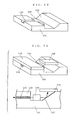
- FIG. 3 is a perspective view illustrating the configuration of an optical package substrate 31 according to a second embodiment of the present invention.
- a guide groove 32 for positioning an optical fiber is formed on the surface of the optical package substrate 31, with a tapered face 33 being formed adjoining the guide groove 32.
- the tapered face 33 constitutes a predetermined angle with respect to the surface of the optical package substrate 31.
- the surface of the package substrate 31 is staggered at the slope 34.
- FIG. 4 is a cross-sectional view illustrating an optical device incorporating the optical package substrate 31 shown in FIG. 3, on which an optical fiber 35 and a surface reception type photodiode 36 are mounted.
- a diffraction grating 37 for causing optical diffraction is provided on the tapered face 33.
- the optical fiber 35 is affixed in the guide groove 32.
- the optical fiber 35 only needs to be placed within the guide groove 32, but is preferably placed in such a manner that an end face thereof abuts against the tapered face 33, as shown in FIG. 4.
- the optical fiber 35 is pressed in place by means of a flat glass plate 38, which in itself is placed so as to abut against the slope 34.
- Above the flat glass plate 38 is mounted a patterned absorption film 39 having an aperture.
- the surface reception type photodiode 36 is mounted in a face-down manner, with a sensor portion thereof being aligned with the aperture in the absorption film 39.
- a positioning marker (not shown) for a light receiving element on the absorption film 39, it becomes particularly easy to mount the surface reception type photodiode 36 through passive alignment.
- the optical fiber 35 and the flat glass plate 38 may be fixed by using UV-curing resin, for example.
- the optical device shown in FIG. 4 incorporating the optical package substrate 31 functions as a light receiving module having a wavelength selecting function.
- the optical package substrate 31 As described above, by employing the optical package substrate 31 according to the second embodiment of the present invention, it is possible to produce an optical device capable of easily deflecting the light which exits the optical fiber 35 and capable of wavelength selection. Moreover, there is no need to watch the rotation of the optical fiber 35 during the mounting of a component.
- the diffraction grating 37 on the tapered face 33 may be formed by directly processing the tapered face 33.
- a diffraction grating which is previously formed on another substrate may be attached by adhering the substrate onto the tapered face 33. It is particularly preferable to form an inverted pattern of a desired diffraction grating on a tapered face of a die for use in the molding of the optical package substrate, and then perform a press formation of the optical package substrate in such a manner that the diffraction grating 37 is molded concurrently with other portions.
- the aforementioned angle of the tapered face 33 is preferably in the range of about 30° to about 70° .
- the aperture of the absorption film 39 may be made narrower, or the thickness of the flat glass plate 38 may be increased.
- the cross section of the guide groove 32 is not limited to a V shape. Rather, any cross sectional shape may be used which permits the optical fiber 35 to be positioned therein, e.g., rectangular, semicircular, or like shapes.
- FIG. 5 is a perspective view illustrating the configuration of an optical package substrate 51 according to a third embodiment of the present invention. As shown in FIG. 5, a guide groove 52 for positioning an optical fiber is formed on the surface of the optical package substrate 51, with a predetermined tapered face 53 being formed adjoining the guide groove 52.
- FIG. 6 is a cross-sectional view illustrating an optical device incorporating the optical package substrate 51 shown in FIG. 5, on which an optical fiber 55 and a surface emission type laser 56 are mounted.
- the optical device structure incorporating the optical package substrate 51 includes a tapered face 53 having a lens-like curvature, with a mirror 57 composed of a thin film capable of reflecting light formed on the surface of the tapered face 53.
- the optical fiber 55 is affixed in the guide groove 52.
- the optical fiber 55 only needs to be placed within the guide groove 52, but is preferably placed in such a manner that an end face thereof abuts against the tapered face 53, as shown in FIG. 6.
- the optical fiber 55 is pressed in place by means of a flat glass plate 58.
- the flat glass plate 58 is positioned by using a marker (not shown) previously provided on the optical package substrate 51.
- the surface emission type laser 56 which is placed in a position for receiving light deflected by the mirror 57 provided on the tapered face 53.
- a positioning marker (not shown) for a light emitting element on the flat glass plate 58
- the optical fiber 55 and the flat glass plate 58 may be fixed by using UV-curing resin, for example.
- the optical device shown in FIG. 6 incorporating the optical package substrate 51 functions as a light transmitting module.
- the optical device can function as a light receiving module for causing light exiting the optical fiber 55 to be reflected and converged by the mirror 57 so as to enter the surface reception type photodiode.
- the optical package substrate 51 As described above, by employing the optical package substrate 51 according to the third embodiment of the present invention, it is possible to produce an optical device capable of easily deflecting the light which exits the surface emission type laser 56 so as to be coupled to the optical fiber 55. Moreover, there is no need to watch the rotation of the optical fiber 55 during the mounting of a component.
- the mirror 57 on the tapered face 53 may be formed by directly applying a metal film through a plating or vacuum process.
- a mirror which is previously formed on another substrate may be attached by adhering the substrate onto the tapered face 53.
- a multilayer film filter which reflects light of a target optical wavelength may be formed on the tapered face 53.
- cross section of the guide groove 52 is not limited to a V shape. Rather, any cross sectional shape may be used which permits the optical fiber 55 to be positioned therein, e.g., rectangular, semicircular, or like shapes.
- first to third embodiments each illustrate an optical package substrate comprising a guide groove for fixing an optical fiber.
- an optical package substrate and an optical device are illustrated which are provided with a waveguide channel corresponding to an optical waveguide core pattern that functions to contain light within the core and allows it to be propagated therethrough in the manner of an optical fiber.
- FIG. 7 is a perspective view illustrating the configuration of an optical package substrate 71 according to a fourth embodiment of the present invention.
- a waveguide channel 72 corresponding to an optical waveguide core pattern is formed on the surface of the optical package substrate 71, with a tapered face 73 being formed adjoining the waveguide channel 72.
- the tapered face 73 constitutes a predetermined angle with respect to the surface of the optical package substrate 71.
- the surface of the optical package substrate 71 is staggered so as to result in a predetermined level difference between a plane on which the waveguide channel 72 is formed and another plane.
- FIG. 8 includes a perspective view and a cross-sectional view illustrating an optical device incorporating the optical package substrate 71 shown in FIG. 7, on which a surface reception type photodiode 76 is mounted.
- FIG. 9A and B shows a cross-sectional view of an optical waveguide formed in the optical package substrate 71.
- a transparent base material 91 with a UV-curing adhesive 92 being thinly applied thereon is prepared.
- the transparent base material 91 has a refractive index similar to that of the optical package substrate 71 in which the waveguide channel 72 is formed, whereas the UV-curing adhesive 92 has a refractive index higher than those of the optical package substrate 71 and the transparent base material 91 (FIG. 9A).
- the transparent base material 91 is attached to the optical package substrate 71 in such a manner that the face on which the UV-curing adhesive 92 is applied faces the waveguide channel 72 (FIG. 9B).
- the transparent base material 91 and the optical package substrate 71 are irradiated with UV rays so that they adhere to each other.
- the UV-curing adhesive 92 embedded within the waveguide channel 72 can be allowed to function as an optical waveguide.
- the flat glass plate 78 is attached to the optical package substrate 71 via a UV-curing adhesive so as to overlie the waveguide channel 72, where the UV-curing adhesive is selected to have a higher refractive index than those of the optical package substrate 71 and the flat glass plate 78, as described above.
- the waveguide channel 72 functions as an optical waveguide.
- the thickness of the flat glass plate 78 is preferably set so that its upper face (as attached to the optical package substrate 71) lies flush with the other plane of the optical package substrate 71.
- a mirror 77 composed of a thin film capable of reflecting light is formed on the tapered face 73.
- the surface reception type photodiode 76 which is placed in a position for receiving light deflected by the mirror 77 provided on the tapered face 73.
- the optical device shown in FIG. 8 incorporating the optical package substrate 71 functions as a light receiving module.
- an optical waveguide can be easily formed, and it is possible to produce an optical device capable of easily deflecting the light which exits the optical waveguide.
- FIG. 10 is a perspective view illustrating the configuration of an optical package substrate 101 according to a fifth embodiment of the present invention.
- a stage 109 for positioning a laser is formed on the surface of the optical package substrate 101, with a tapered face 103 being formed.
- the tapered face 103 constitutes a predetermined angle with respect to the surface of the optical package substrate 101.
- the surface of the optical package substrate 101 is staggered so as to result in a predetermined level difference between a plane on which the stage 109 is formed and another plane.
- FIG. 11 includes a perspective view and a cross-sectional view illustrating an optical device incorporating the optical package substrate 101 shown in FIG. 10, on which a waveguide type laser 110 and a surface reception type photodiode 106 are mounted.
- the optical device structure incorporating the optical package substrate 101 includes a mirror 107 composed of a thin film capable of reflecting light, which is formed on the tapered face 103.
- the waveguide type laser 110 is mounted on the stage 109 through passive alignment, with reference to a positioning marker (not shown) provided on the stage 109.
- the plane of the optical package substrate 101 on which the stage 109 is formed is configured so that light exiting the waveguide type laser 110 placed thereon is incident on the tapered face 103.
- the surface reception type photodiode 106 is also mounted through passive alignment, with reference to a positioning marker (not shown) provided on the optical package substrate 101, so as to be placed in a position for receiving light deflected by the mirror 107 provided on the tapered face 103.
- principal light which is emitted from the waveguide type laser 110 in the left direction in FIG. 11 is coupled to an optical fiber (not shown) via a lens or the like, whereas subordinate light which is emitted in the right direction in FIG. 11 is reflected from the mirror 107 provided on the tapered face 103, so as to enter the surface reception type photodiode 106 (see the arrows in FIG. 11).
- the optical device shown in FIG. 11 incorporating the optical package substrate 101 functions as a light transmitting module which permits the optical output from the waveguide type laser 110 to be monitored.
- the optical package substrate 101 As described above, by employing the optical package substrate 101 according to the fifth embodiment of the present invention, it is possible to produce an optical device capable of easily deflecting the light which is emitted from the waveguide type laser 110 and permitting the intensity of the laser light to be monitored.
- FIG. 12 is a perspective view illustrating the configuration of an optical package substrate 121 according to a sixth embodiment of the present invention.
- a waveguide channel 122 corresponding to an optical waveguide core pattern and a stage 129 for positioning a laser are formed on the surface of the optical package substrate 121, with a tapered face 123 also being formed.
- the tapered face 123 constitutes a predetermined angle with respect to the surface of the optical package substrate 121.
- the surface of the optical package substrate 121 is staggered so as to result in predetermined level differences between a plane on which waveguide channel 122 is formed, a plane on which the stage 129 is formed, and another plane.
- FIG. 13 includes a perspective view and a cross-sectional view illustrating an optical device incorporating the optical package substrate 121 shown in FIG. 12, on which a waveguide type laser 130 and a surface reception type photodiode 126 are mounted.
- the flat glass plate 128 is attached to the optical package substrate 121 via a UV-curing adhesive so as to overlie the waveguide channel 122, where the UV-curing adhesive is selected to have a higher refractive index than those of the optical package substrate 121 and the flat glass plate 128, as in the fourth embodiment.
- the waveguide channel 122 functions as an optical waveguide.
- the waveguide type laser 130 is mounted on the stage 129 through passive alignment, with reference to a positioning marker (not shown) provided on the stage 129.
- the plane of the optical package substrate 121 on which the stage 129 is formed is configured so that the optical axis of principal light which is emitted from the waveguide type laser 130 placed thereon coincides with the optical axis of the optical waveguide defined in the waveguide channel 122, and that the optical axis of subordinate light is incident on the tapered face 123.
- a mirror 127 composed of a thin film capable of reflecting light is formed on the tapered face 123.
- the surface reception type photodiode 126 is mounted through passive alignment, with reference to a positioning marker (not shown) provided on the optical package substrate 121, so as to be placed in a position for receiving light deflected by the mirror 127 provided on the tapered face 123.
- the optical device shown in FIG. 13 incorporating the optical package substrate 121 functions as a light transmitting module which combines the functions of the optical devices according to the fourth and fifth embodiments.
- an optical waveguide can be easily formed, and it is possible to produce an optical device capable of coupling principal light emitted from the waveguide type laser 130 to the optical waveguide, easily deflecting the subordinate light, and permitting the intensity of the laser light to be monitored.
- the mirror 77,107, or 127 provided on the tapered face 73,103, or 123 may be formed by directly applying a metal film through a plating or vacuum process.
- a mirror which is previously formed on another substrate may be attached by adhering the substrate onto the tapered face.
- a multilayer film filter which reflects light of a target optical wavelength may be formed on the tapered face.
- the aforementioned angle of the tapered face 73, 103, or 123 is preferably in the range of about 30° to about 70° .
- the angle is about 60° or more as to minimize any fluctuations in characteristics associated with polarization.
- the tapered face may alternatively be a curved surface.
- a preferable method for molding the optical package substrates according to the first to sixth embodiments will be described.
- a die for use in the molding of an optical package substrate is produced, and this resultant die is pressed against a glass material which has been softened by being heated to a high temperature so as to transcribe the configuration of the die to the glass material (press formation), whereby the optical package substrate is molded.
- glass material which is thermally, mechanically, and chemically stable is preferable as the material of the optical package substrate, any other material which permits press formation can also be used.
- the inventors have confirmed through experimentation that press formation can be successfully performed by pressing an ultra-hard alloy die, on which a protective film composed of a precious metal alloy is formed, against an optical glass substrate which is heated to 580°C in a nitrogen gas atmosphere.
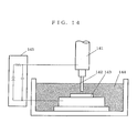
- FIG. 14 is a schematic diagram illustrating general principles of discharge machining.
- a tool electrode 142 attached at the tip of a mandrel 141, which defines a rotation axis, and a work 143 (which functions as an electrode) as an object to be processed are immersed in an insulation liquid 144.
- the two electrodes are brought close to each other while applying a predetermined voltage between the tool electrode 142 and the work 143 by means of a discharge generation section 145, thereby causing an electrical discharge through which the work 143 is melted away.
- the tool electrode 142 is further advanced by a corresponding distance. This process is repeated in order to process the work 143 into a desired configuration.
- a microdischarge machining technique which is based on similar processing principles, utilizes a special discharge circuit to provide a discharge energy which is about 1/100 of what is normally used, thereby realizing coarse processing on the order of microns and fine processing on the order of sub-microns.
- This microdischarge machining technique mainly has the following features:
- a tool electrode of any configuration e.g., triangular prism or a rectangular prism as well as a cylinder
- a tool electrode can be realized in units of several millimeters or more.
- the tip of a tool electrode composed of sintered diamond or the like can be fine-processed into a cylindrical or conical shape, such a tool electrode can be used for microgrinding a die.
- a processing method which can be adopted in the fine processing of a tool electrode is in itself disclosed in Japanese Patent Laid-Open Publication No. 2001-54808.
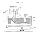
- a shaft-like tool material 152 which is to be processed, is attached to the tip of the mandrel 151.
- the position of the tool material 152 can be moved up or down along the rotation axis direction by means of a Z stage 157 equipped with a motor 156.
- a processing bath 159 which is placed on an X-Y stage 158, an electrode plate 153 for discharge machining is fixed.
- the electrode plate 153 for discharge machining is fixed so as to be parallel to the Y axis and at an angle of 45° to the X-Y plane.
- the inside of the processing bath 159 is filled with an insulation liquid 154.
- a discharge generation section 155 composed of an RC circuit capable of generating discharge pulses of a minute energy level is coupled between the tool material 152 and the electrode plate 153 for discharge machining.
- a microdischarge machining on the order of ⁇ m for the tool material 152.
- the tip of the tool material 152 can be processed into a desired configuration through microdischarge machining while sending the tool material 152, which is rotated (or reciprocated), toward the electrode plate 153 for discharge machining by means of the Z stage 157.
- FIG. 15 illustrates an example where the tool material 152 is processed so as to have a conical tip while being rotated. Note that sintered diamond for which a metal has been used as a binder can be employed as the tool material 152 because such sintered diamond is electrically conductive.
- the processed tool material 152 i.e., the tool electrode
- the work 160 which has previously been fixed in the processing bath 159, and positioned in place.
- This positioning can be achieved by detecting electrical conduction between the tool electrode and the work 160 and the two are gradually brought near.
- the tool electrode and is moved in a desired direction while being rotated, so as to be pressed against a portion previously processed on the surface of the work 160 which requires precision finishing (i.e., the slopes of a V-shaped protrusion in the example shown in FIG. 15).
- the shaping precision and planar precision of the desired portion i.e., the slopes of the V-shaped protrusion in this example
- the shaping precision and planar precision of the desired portion i.e., the slopes of the V-shaped protrusion in this example
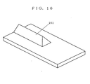
- a die to be used for the molding of the optical package substrate 11 according to the first embodiment would have a configuration as shown in FIG. 16, such that a protrusion 161 for molding the guide groove 12 is provided on the surface thereof.
- a tool electrode 171 having the shape of a triangular prism and a scalpel-shaped tool electrode 172 as shown in FIG. 17A are first produced.
- a microdischarge machining process is first performed by using the tool electrode 171 while maintaining the work 173 in an upright position (as shown in the left-hand side of FIG.
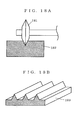
- FIGS. 18A and 18B For comparison, a conventional die processing method for molding a general V groove which utilizes a microgrinder will be described with reference to FIGS. 18A and 18B.
- a circular diamond grindstone 181 having a V-shaped edge is employed as a grindstone for a microgrinder. As shown in FIG. 18A, by performing grinding process with a this grindstone 181 from an end of a plane-like ultra-hard alloy 182, a die 183 as shown in FIG. 18B can be obtained.
- an ultra-hard alloy is exemplified as a die material in the above description, any electrically conductive material having a sufficient heat resistance and mechanical strength can be used, e.g., SUS.
- an ultra-hard alloy or the like may be used as a parent material for a die; an electrically conductive film such as a precious metal alloy film may be formed on the surface thereof; and this film may be processed into a desired configuration.
Landscapes
- Physics & Mathematics (AREA)
- General Physics & Mathematics (AREA)
- Optics & Photonics (AREA)
- Engineering & Computer Science (AREA)
- Microelectronics & Electronic Packaging (AREA)
- Optical Couplings Of Light Guides (AREA)
- Optical Integrated Circuits (AREA)
- Light Receiving Elements (AREA)
- Electroluminescent Light Sources (AREA)
- Semiconductor Lasers (AREA)
Abstract
There is provided an optical package substrate and a molding method therefor, which provides for easy production, easy mounting of optical elements such as photodiodes and lasers, good functionality, productivity, and economy, as well as an optical device incorporating the package substrate. On the surface of an optical package substrate (11), a guide groove (12) used for the positioning of an optical fiber and a tapered face (13) adjoining the guide groove (12) are provided, the tapered face (13) being formed so as to have a predetermined angle. A mirror (17) for reflecting light is formed on the tapered face (13). An optical fiber (15) is affixed in the guide groove (12). Above the tapered face (13) is mounted a surface reception type photodiode (16), which is placed in a position for receiving light deflected by the mirror (17) provided on the tapered face (13). By providing a positioning marker (not shown) for a light receiving element on the optical package substrate (11), it becomes particularly easy to mount the surface reception type photodiode (16) through passive alignment.
Description
The present invention relates to an optical package
substrate and an optical device, and more particularly to a
package substrate having a surface configuration suitable for
mounting optical components and/or optical elements thereon, and
a molding method for such a package substrate; and an optical
device constructed by employing the package substrate.
Optical communication systems employing optical fibers
are evolving themselves from conventional long haul communication
systems into subscriber communication systems. Subscriber-type
optical communication systems require the use of small and
inexpensive optical devices.
In conventional optical devices, optical components
such as optical fibers and/or lenses and optical elements such
as lasers and/or photodiodes are deployed in a coaxial arrangement.
Usually, the positioning of optical fibers and lenses requires
a high precision, e.g., a tolerance of ±1µm. Therefore, a
so-called active alignment technique has been used for the
assembly of an optical device, where the positioning of the
components is adjusted while driving the optical elements with
laser light actually being led therethrough. However, this
technique requires complicated tasks, and is time-consuming, thus
presenting a substantial cost problem.
On the other hand, so-called passive alignment, in
which the components are positioned without the aforementioned
adjustment has attracted attention as a technique for simplifying
the assembly of an optical device. Typical examples of this
technique are used in optical devices such that light guided
through optical fibers and optical cavities is deflected by 90°
so as to be received by a photodiode of a surface reception type.
Various ideas have been proposed for this technique, in documents
such as Japanese Patent Laid-Open Publication No. 11-326662 and
Japanese Patent No. 2687859.
FIG. 19 is a cross-sectional view showing an exemplary
optical device structure which utilizes a conventionally-proposed
deflection method.
As shown in FIG. 19, an end face of an optical fiber
(or an optical waveguide) 191 is ground at 45° , with a reflection
mirror 192 being provided on this end face. Light guided through
the optical fiber (optical waveguide) 191 which is incident from
the left direction in FIG. 19 has its optical path turned (i.e.,
deflected) by 90° at the mirror 192, so as to be received by the
photodiode 193. The photodiode 193 may be of a surface reception
type as that shown in FIG. 19, or of a different type called a
"waveguide type".
A surface reception type photodiode has a large area
for receiving light, so that it only requires a positioning
precision of only about ± tens of microns (µm) with respect to
an optical fiber or an optical waveguide. Therefore, the mounting
of a surface reception type photodiode can be realized through
a passive alignment, which involves forming markers on the
substrate as reference points for the mounting process. However,
when light which is guided through the optical fiber or optical
waveguide needs to be received directly at the front face of the
surface reception type photodiode, it is necessary to mount the
surface reception type photodiode in an upright position on the
substrate, which makes mass production more difficult. An
example of this situation is monitoring of a laser output, where
surface reception type photodiodes are a common choice.
On the other hand, a waveguide type photodiode has a
light receiving layer on the order of several microns. Therefore,
a positioning precision as stringent as ±1µm is required in order
to ensure that light guided through an optical fiber or optical
waveguide is properly coupled to a waveguide type photodiode.
Thus, active alignment is usually employed for waveguide type
photodiodes, thereby presenting a substantial mounting cost
problem.
Thus, it can be seen that the construction shown in
FIG. 19, where light which exits from an optical fiber or optical
waveguide is deflected by 90° , can be highly effective in terms
of mass production and mounting costs, because it makes it
possible to mount a surface reception type photodiode in a
face-down manner through passive alignment.
FIG 20 shows another exemplary optical device
structure utilizing the conventional deflection method
described in Japanese Patent Laid-Open Publication No. 11-326662.
Referring to FIG. 20, this optical device features a
reflective member 201, which is formed by processing a portion
of an optical waveguide into a reflective surface for reflecting
light. Light which is propagated through the waveguide layer 202
to exit at its end face is deflected by 90° , so as to be received
by a surface reception type photodiode 203.
As illustrated by the above two examples, conventional
optical device structures are based on the concept of deflecting
an optical path of light exiting from an optical fiber or optical
waveguide so as to allow the exiting light to be received by a
surface reception type photodiode, which requires a relatively
low receiving positioning precision, with a view to reducing the
device cost.
However, the conventional optical device structures
illustrated in FIGS. 19 and 20 require an additional process of
working an end face of an optical fiber (or an optical waveguide)
into a face having a 45° slope. Moreover, in order to minimize
the scattering loss at the processed surface, it is essential to
secure a high planar precision, so that processes such as grinding,
dry etching, wet etching, and cutting must be carried out with
a good reproducibility. Especially in the case where an optical
fiber processed so as to have a slanting end face is employed,
light exiting from the optical fiber may not be properly incident
on a photodiode if the optical fiber fails to be mounted in the
correct orientation, due to rotation or the like.
Thus, while conventional optical device structures
provide advantages associated with simplified photodiode
mounting, they also require additional processing steps, which
detract from the cost advantages.
Therefore, the objectives of the present invention are
to provide an easy-to-manufacture optical package substrate which
allows for easy mounting of optical elements such as photodiodes
and lasers, and which is excellent in functionality,
producibility, and economy, and a molding method for such an
optical package substrate; and to provide an optical device
constructed by employing the package substrate.
The present invention has the following features to
attain the above object.
A first aspect of the present invention is directed to
an optical package substrate for mounting an optical component
and/or an optical element thereon, comprising: a guide section
for fixing an optical axis of an optical fiber mounted in the guide
section, the guide section being a groove formed on a surface of
a substrate and extending from an end face of the substrate to
a predetermined portion of the substrate; and an optical path
deflection section for deflecting an optical path by reflection,
the optical path deflection section being formed at the
predetermined portion of the guide section so as to be in a position
intersecting the optical axis of the optical fiber mounted in the
guide section.
Thus, according to the first aspect, a guide section
used for the positioning of an optical fiber, and an optical path
deflection section for deflecting light through reflection are
concurrently molded onto an optical package substrate. As a
result, a passive alignment of an optical component and an optical
element can be easily realized without requiring any additional
processing steps.
A second aspect according to the present invention is
directed to an optical package substrate for mounting an optical
component and/or an optical element thereon, comprising: a
waveguide section as a groove formed on a surface of a substrate
and extending from an end face of the substrate to a predetermined
portion of the substrate, the waveguide section corresponding to
a predetermined optical waveguide core pattern; and an optical
path deflection section for deflecting an optical path by
reflection, the optical path deflection section being formed at
the predetermined portion of the waveguide section so as to be
in a position intersecting an optical axis of the optical
waveguide defined in the waveguide section.
Thus, according to the second aspect, a waveguide
section corresponding to an optical waveguide core pattern and
an optical path deflection section for deflecting light through
reflection are concurrently molded onto an optical package
substrate. As a result, a passive alignment of an optical
component and an optical element can be easily realized without
requiring any additional processing steps.
A third aspect according to the present invention is
directed to an optical package substrate for mounting an optical
component and/or an optical element thereon, comprising: a stage
portion for fixing an optical axis of a light receiving/emitting
element mounted on the stage portion, the stage portion being
formed on a surface of a substrate; and an optical path deflection
section for deflecting an optical path by reflection, the optical
path deflection section being formed on the surface of the
substrate so as to be in a position intersecting the optical axis
of the light receiving/emitting element mounted on the stage
portion.
Thus, according to the third aspect, a stage portion,
used for the positioning of a light receiving/emitting element
and an optical path deflection section for deflecting light
through reflection are concurrently molded onto an optical
package substrate. As a result, a passive alignment of an optical
component and an optical element can be easily realized without
requiring any additional processing steps.
According to a fourth aspect according to the present
invention based on the third aspect, a waveguide section is
further comprised which is formed on the surface of the substrate,
the waveguide section corresponding to an optical waveguide core
pattern having an optical axis coinciding with an optical axis
of the light receiving/emitting element mounted on the stage
portion.
Thus, according to the fourth aspect, a waveguide
section corresponding to an optical waveguide core pattern, a
stage portion, and an optical path deflection section are
concurrently molded onto an optical package substrate. As a
result, a passive alignment of an optical component and an optical
element can be easily realized without requiring any additional
processing steps.
Preferably, a thin film element having a mirror
property is provided on the optical path deflection section. As
a result, it becomes possible not only to merely reflect light
at the optical path deflection section, but also obtain a
different reflectance depending on the wavelength of light.
Alternatively, a diffraction grating for creating
different optical paths for different optical wavelengths is
provided on the optical path deflection section. As a result,
by utilizing the properties of a diffraction grating having
different diffraction angles for different wavelengths, an
optical device comprising a filtering function for receiving
light of only a specific wavelength can be realized.
Alternatively, the optical path deflection section has
a curvature for converging a plurality of incident rays through
reflection. As a result, the positioning precision for a light
receiving element can be further relaxed, or light emitted from
a surface emission type light emitting element can be converged
so as to be coupled to an optical fiber or an optical waveguide
with a high efficiency.
The optical package substrate preferably comprises
glass. By employing glass, it becomes possible to form highly
precise configuration on a surface by means of a die, and excellent
stability can be provided in various environments. Since glass
is transmissive to UV rays, the fixing of an optical fiber or the
like can be achieved by using a UV-curing adhesive, instead of
a time-consuming thermosetting adhesive.
Furthermore, the optical package substrate may be
molded by pressing a die against a substrate material softened
by being heated to a high temperature to transcribe an inverted
pattern of the die onto the substrate material, the die having
been obtained by using a normal-grinding tool and an arbitrary
fine-grinding tool, wherein at least one of the die and the
fine-grinding tool is obtained through microdischarge machining.
By producing a die having a complicated configuration
through microdischarge machining employing this method for
producing an optical package substrate, which would have been
highly difficult to obtain by a conventional grinding process,
the optical package substrate according to the present invention
can be obtained.
A fifth aspect according to the present invention is
directed to an optical device having an optical component and/or
optical element mounted on an optical package substrate, the
optical package substrate comprising: a guide section for fixing
an optical axis of an optical fiber mounted in the guide section,
the guide section being a groove formed on a surface of a substrate
and extending from an end face of the substrate to a predetermined
portion of the substrate; and an optical path deflection section
for deflecting an optical path by reflection, the optical path
deflection section being formed at the predetermined portion of
the guide section so as to be in a position intersecting the optical
axis of the optical fiber mounted in the guide section, wherein
the optical fiber placed in the guide section on the optical
package substrate is pressed from above by a predetermined
substrate, whereby the optical fiber is affixed to the optical
package substrate.
Thus, according to the fifth aspect, an optical fiber
can be firmly mounted on an optical package substrate, and an
optical device capable of deflecting light propagated through an
optical fiber can be produced from the optical package substrate
through very simple steps, leading to excellent productivity and
economy. It is also possible to employ a predetermined
substrate as a stage on which to mount a photodiode, a laser, or
the like.
A sixth aspect according to the present invention is
directed to an optical device having an optical component and/or
optical element mounted on an optical package substrate, the
optical package substrate comprising: a waveguide section as a
groove formed on a surface of a substrate and extending from an
end face of the substrate to a predetermined portion of the
substrate, the waveguide section corresponding to a predetermined
optical waveguide core pattern; and an optical path deflection
section for deflecting an optical path by reflection, the optical
path deflection section being formed at the predetermined portion
of the waveguide section so as to be in a position intersecting
an optical axis of the optical waveguide defined in the waveguide
section, the optical device further comprising a predetermined
substrate, wherein a core material having a refractive index
higher than a refractive index of the optical package substrate
is filled in the waveguide section of the optical package
substrate, and thereafter an adhesive having a refractive index
lower than the refractive index of the core material is used to
attach the predetermined substrate to the waveguide section.
Thus, according to the sixth aspect, by filling a core
material having a high refractive index in a waveguide section
so that the waveguide section functions as an optical waveguide,
an optical device capable of deflecting light propagated through
an optical fiber can be produced from the optical package
substrate through very simple steps, leading to excellent
productivity and economy.
A seventh aspect according to the present invention is
directed to an optical device having an optical component and/or
optical element mounted on an optical package substrate, the
optical package substrate comprising: a stage portion for fixing
an optical axis of a light receiving/emitting element mounted on
the stage portion, the stage portion being formed on a surface
of a substrate; and an optical path deflection section for
deflecting an optical path by reflection, the optical path
deflection section being formed on the surface of the substrate
so as to be in a position intersecting the optical axis of the
light receiving/emitting element mounted on the stage portion
wherein the light receiving/emitting element is affixed to the
stage portion on the optical package substrate.
Thus, according to the seventh aspect, an optical
device capable of realizing optical coupling between a light
receiving/emitting element and another optical element can be
produced from an optical package substrate through very simple
steps, by simply affixing a light receiving/emitting element on
a stage portion through passive alignment. Thus, excellent
productivity and economy can be obtained.
According to an eighth aspect according to the present
invention based on the seventh aspect, the optical package
substrate further comprises a waveguide section formed on the
surface of the substrate, the waveguide section corresponding to
an optical waveguide core pattern having an optical axis
coinciding with an optical axis of the light receiving/emitting
element mounted on the stage portion, the optical device further
comprising a predetermined substrate, wherein a core material
having a refractive index higher than a refractive index of the
optical package substrate is filled in the waveguide section of
the optical package substrate, and thereafter an adhesive having
a refractive index lower than the refractive index of the core
material is used to attach the predetermined substrate to the
waveguide section.
Thus, according to the eighth aspect, an optical
device capable of realizing optical coupling between a light
receiving/emitting element and another optical element can be
produced from an optical package substrate through very simple
steps, by simply affixing a light receiving/emitting element on
a stage portion through passive alignment. Thus, excellent
productivity and economy can be obtained.
The optical device may further comprise a surface
mounting type light receiving/emitting element which is optically
coupled to the optical fiber affixed in the guide section through
the optical path deflected by the optical path deflection section.
Alternatively, the optical device may further comprise a surface
mounting type light receiving/emitting element which is optically
coupled to the optical waveguide defined in the waveguide section
through the optical path deflected by the optical path deflection
section. Alternatively, the optical device may further comprise
a surface mounting type light receiving/emitting element which
is optically coupled to the light receiving/emitting element
affixed to the stage portion through the optical path deflected
by the optical path deflection section. Thus, since the light
receiving/emitting element is of a surface mounting type, the
light receiving/emitting element can be mounted even with a
relaxed positioning precision. As a result, adjustment-free
mounting can be easily realized.
These and other objects, features, aspects and
advantages of the present invention will become more apparent from
the following detailed description of the present invention when
taken in conjunction with the accompanying drawings.
Hereinafter, illustrative embodiments of the present
invention will be described with reference to the figures.
FIG. 1 is a perspective view illustrating the
configuration of an optical package substrate 11 according to a
first embodiment of the present invention. As shown in FIG. 1,
a guide groove 12 for positioning an optical fiber is formed on
the surface of the optical package substrate 11, with a tapered
face 13 being formed adjoining the guide groove 12. The tapered
face 13 constitutes a predetermined angle with respect to the
surface of the optical package substrate 11.
FIG. 2 is a cross-sectional view illustrating an
optical device incorporating the optical package substrate 11 of
FIG. 1, with an optical fiber 15 and a surface reception type
photodiode 16 being mounted thereon.
As shown in FIG. 2, the optical device structure
incorporating the optical package substrate 11 includes a mirror
17 composed of a thin film capable of reflecting light, which is
formed on the tapered face 13. The optical fiber 15 is affixed
in the guide groove 12 by using an ultraviolet (UV) -curing resin,
for example. The optical fiber 15 only needs to be placed within
the guide groove 12, but is preferably placed in such a manner
that an end face thereof abuts against the tapered face 13, as
shown in FIG. 2. Above the tapered face 13 is mounted the surface
reception type photodiode 16, which is placed in a position for
receiving light deflected by the mirror 17 provided on the tapered
face 13. By providing a positioning marker (not shown) for a light
receiving element on the optical package substrate 11, it becomes
particularly easy to mount the surface reception type photodiode
16 through passive alignment.
In accordance with this structure, light which is
propagated through the optical fiber 15 in the left to right
direction in FIG. 2 exits the optical fiber 15 at its right end
face, and thereafter is reflected from the mirror 17 provided on
the tapered face 13, so as to enter the surface reception type
photodiode 16 (see the arrow in FIG. 2). Thus, the optical device
shown in FIG. 2 incorporating the optical package substrate 11
functions as a light receiving module.
As described above, by employing the optical package
substrate 11 according to the first embodiment of the present
invention, it is possible to produce an optical device capable
of easily deflecting the light which exits the optical fiber 15.
Moreover, there is no need to watch the rotation of the optical
fiber 15 during the mounting of a component.
The mirror 17 on the tapered face 13 may be formed by
directly applying a metal film through a plating or vacuum process.
Alternatively, a mirror which is previously formed on another
substrate may be attached by adhering the substrate onto the
tapered face 13. Instead of a mirror, a multilayer film filter
which reflects light of a target optical wavelength may be formed
on the tapered face 13.
In practice, the aforementioned angle of the tapered
face 13 is preferably in the range of about 30° to about 70° .
In particular, in the case where a multilayer film filter is formed
on the tapered face 13, it is preferable that the angle is about
60° or more as to minimize any fluctuations in characteristics
associated with polarization.
Furthermore, the cross section of the guide groove 12
is not limited to a V shape. Rather, any cross sectional shape
may be used which permits the optical fiber 15 to be positioned
therein, e.g., rectangular, semicircular, or like shapes.
Instead of the aforementioned optical fiber 15, an
optical fiber 191 shown in FIG. 19 may be employed, which is
provided with a mirror that is ground at a predetermined angle
on one end face; in this case, it is unnecessary to form the mirror
17 on the tapered face 13. Even when such an optical fiber 191
is employed, the tapered face 13 formed on the optical package
substrate 11 prevents the rotation of the optical fiber 191 during
the mounting of a component.
FIG. 3 is a perspective view illustrating the
configuration of an optical package substrate 31 according to a
second embodiment of the present invention. As shown in FIG. 3,
a guide groove 32 for positioning an optical fiber is formed on
the surface of the optical package substrate 31, with a tapered
face 33 being formed adjoining the guide groove 32. The tapered
face 33 constitutes a predetermined angle with respect to the
surface of the optical package substrate 31. The surface of the
package substrate 31 is staggered at the slope 34.
FIG. 4 is a cross-sectional view illustrating an
optical device incorporating the optical package substrate 31
shown in FIG. 3, on which an optical fiber 35 and a surface
reception type photodiode 36 are mounted.
In the optical device structure shown in FIG. 4
incorporating the optical package substrate 31, a diffraction
grating 37 for causing optical diffraction is provided on the
tapered face 33. The optical fiber 35 is affixed in the guide
groove 32. The optical fiber 35 only needs to be placed within
the guide groove 32, but is preferably placed in such a manner
that an end face thereof abuts against the tapered face 33, as
shown in FIG. 4. The optical fiber 35 is pressed in place by means
of a flat glass plate 38, which in itself is placed so as to abut
against the slope 34. Above the flat glass plate 38 is mounted
a patterned absorption film 39 having an aperture. The surface
reception type photodiode 36 is mounted in a face-down manner,
with a sensor portion thereof being aligned with the aperture in
the absorption film 39. By providing a positioning marker (not
shown) for a light receiving element on the absorption film 39,
it becomes particularly easy to mount the surface reception type
photodiode 36 through passive alignment. The optical fiber 35
and the flat glass plate 38 may be fixed by using UV-curing resin,
for example.
In accordance with this structure, light which is
propagated through the optical fiber 35 in the left to right
direction in FIG. 4 exits the optical fiber 35 at its right end
face, and thereafter is diffracted by the diffraction grating 37
provided on the tapered face 33. The diffraction grating 37
functions to provide different diffraction angles depending on
the wavelength of light. Therefore, by inserting the absorption
film 39 between the diffraction grating 37 and the surface
reception type photodiode 36, it becomes possible to ensure that
light of only a specific wavelength is received at the surface
reception type photodiode 36 (see the arrows in FIG. 4). Thus,
the optical device shown in FIG. 4 incorporating the optical
package substrate 31 functions as a light receiving module having
a wavelength selecting function.
As described above, by employing the optical package
substrate 31 according to the second embodiment of the present
invention, it is possible to produce an optical device capable
of easily deflecting the light which exits the optical fiber 35
and capable of wavelength selection. Moreover, there is no need
to watch the rotation of the optical fiber 35 during the mounting
of a component.
The diffraction grating 37 on the tapered face 33 may
be formed by directly processing the tapered face 33.
Alternatively, a diffraction grating which is previously formed
on another substrate may be attached by adhering the substrate
onto the tapered face 33. It is particularly preferable to form
an inverted pattern of a desired diffraction grating on a tapered
face of a die for use in the molding of the optical package
substrate, and then perform a press formation of the optical
package substrate in such a manner that the diffraction grating
37 is molded concurrently with other portions.
In practice, the aforementioned angle of the tapered
face 33 is preferably in the range of about 30° to about 70° .
In order to enhance the accuracy of wavelength
separation, the aperture of the absorption film 39 may be made
narrower, or the thickness of the flat glass plate 38 may be
increased.
Furthermore, the cross section of the guide groove 32
is not limited to a V shape. Rather, any cross sectional shape
may be used which permits the optical fiber 35 to be positioned
therein, e.g., rectangular, semicircular, or like shapes.
FIG. 5 is a perspective view illustrating the
configuration of an optical package substrate 51 according to a
third embodiment of the present invention. As shown in FIG. 5,
a guide groove 52 for positioning an optical fiber is formed on
the surface of the optical package substrate 51, with a
predetermined tapered face 53 being formed adjoining the guide
groove 52.
FIG. 6 is a cross-sectional view illustrating an
optical device incorporating the optical package substrate 51
shown in FIG. 5, on which an optical fiber 55 and a surface emission
type laser 56 are mounted.
As shown in FIG. 6, the optical device structure
incorporating the optical package substrate 51 includes a tapered
face 53 having a lens-like curvature, with a mirror 57 composed
of a thin film capable of reflecting light formed on the surface
of the tapered face 53. The optical fiber 55 is affixed in the
guide groove 52. The optical fiber 55 only needs to be placed
within the guide groove 52, but is preferably placed in such a
manner that an end face thereof abuts against the tapered face
53, as shown in FIG. 6. The optical fiber 55 is pressed in place
by means of a flat glass plate 58. The flat glass plate 58 is
positioned by using a marker (not shown) previously provided on
the optical package substrate 51. Above the flat glass plate
58 is mounted the surface emission type laser 56, which is placed
in a position for receiving light deflected by the mirror 57
provided on the tapered face 53. By providing a positioning
marker (not shown) for a light emitting element on the flat glass
plate 58, it becomes easy to mount the surface emission type laser
56 through passive alignment. In other words, by performing the
alignment between the flat glass plate 58 and the optical package
substrate 51 and the alignment between the flat glass plate 58
and the surface emission type laser 56 each based on a marker,
it becomes possible to align the surface emission type laser 56
with respect to the optical package substrate 51. The optical
fiber 55 and the flat glass plate 58 may be fixed by using UV-curing
resin, for example.
In accordance with this structure, light exiting the
surface emission type laser 56 arrives at the tapered face 53 as
it spreads out. The arriving light is reflected and converged
by the mirror 57 provided on the tapered face 53, so as to be coupled
to the optical fiber 55 (see the arrows in FIG. 6). Thus, the
optical device shown in FIG. 6 incorporating the optical package
substrate 51 functions as a light transmitting module.
By replacing the surface emission type laser 56 with
a surface reception type photodiode, the optical device can
function as a light receiving module for causing light exiting
the optical fiber 55 to be reflected and converged by the mirror
57 so as to enter the surface reception type photodiode.
As described above, by employing the optical package
substrate 51 according to the third embodiment of the present
invention, it is possible to produce an optical device capable
of easily deflecting the light which exits the surface emission
type laser 56 so as to be coupled to the optical fiber 55. Moreover,
there is no need to watch the rotation of the optical fiber 55
during the mounting of a component.
The mirror 57 on the tapered face 53 may be formed by
directly applying a metal film through a plating or vacuum process.
Alternatively, a mirror which is previously formed on another
substrate may be attached by adhering the substrate onto the
tapered face 53. Instead of a mirror, a multilayer film filter
which reflects light of a target optical wavelength may be formed
on the tapered face 53.
Furthermore, the cross section of the guide groove 52
is not limited to a V shape. Rather, any cross sectional shape
may be used which permits the optical fiber 55 to be positioned
therein, e.g., rectangular, semicircular, or like shapes.
The above-described first to third embodiments each
illustrate an optical package substrate comprising a guide groove
for fixing an optical fiber. In each of Lhe following embodiments,
an optical package substrate and an optical device are illustrated
which are provided with a waveguide channel corresponding to an
optical waveguide core pattern that functions to contain light
within the core and allows it to be propagated therethrough in
the manner of an optical fiber.
FIG. 7 is a perspective view illustrating the
configuration of an optical package substrate 71 according to a
fourth embodiment of the present invention. As shown in FIG. 7,
a waveguide channel 72 corresponding to an optical waveguide core
pattern is formed on the surface of the optical package substrate
71, with a tapered face 73 being formed adjoining the waveguide
channel 72. The tapered face 73 constitutes a predetermined angle
with respect to the surface of the optical package substrate 71.
The surface of the optical package substrate 71 is staggered so
as to result in a predetermined level difference between a plane
on which the waveguide channel 72 is formed and another plane.
FIG. 8 includes a perspective view and a cross-sectional
view illustrating an optical device incorporating the
optical package substrate 71 shown in FIG. 7, on which a surface
reception type photodiode 76 is mounted.
Now, a method for forming an optical waveguide in the
waveguide channel 72 will be described with reference to FIG. 9A
and B. FIG. 9A and B shows a cross-sectional view of an optical
waveguide formed in the optical package substrate 71.
First, a transparent base material 91 with a UV-curing
adhesive 92 being thinly applied thereon is prepared. The
transparent base material 91 has a refractive index similar to
that of the optical package substrate 71 in which the waveguide
channel 72 is formed, whereas the UV-curing adhesive 92 has a
refractive index higher than those of the optical package
substrate 71 and the transparent base material 91 (FIG. 9A). Then,
the transparent base material 91 is attached to the optical
package substrate 71 in such a manner that the face on which the
UV-curing adhesive 92 is applied faces the waveguide channel 72
(FIG. 9B). Finally, the transparent base material 91 and the
optical package substrate 71 are irradiated with UV rays so that
they adhere to each other. According to this formation method,
by ensuring that the layer of adhesive which is present in portions
other than the waveguide channel 72 created as a result of the
above attachment is sufficiently thin, the UV-curing adhesive 92
embedded within the waveguide channel 72 can be allowed to
function as an optical waveguide.
In the optical device structure incorporating the
optical package substrate 71 illustrated in FIG. 8, the flat glass
plate 78 is attached to the optical package substrate 71 via a
UV-curing adhesive so as to overlie the waveguide channel 72,
where the UV-curing adhesive is selected to have a higher
refractive index than those of the optical package substrate 71
and the flat glass plate 78, as described above. As a result,
the waveguide channel 72 functions as an optical waveguide. The
thickness of the flat glass plate 78 is preferably set so that
its upper face (as attached to the optical package substrate 71)
lies flush with the other plane of the optical package substrate
71. A mirror 77 composed of a thin film capable of reflecting
light is formed on the tapered face 73. Above the optical package
substrate 71 and the flat glass plate 78 is formed the surface
reception type photodiode 76, which is placed in a position for
receiving light deflected by the mirror 77 provided on the tapered
face 73. By providing a positioning marker (not shown) for a light
receiving element on the optical package substrate 71 or the flat
glass plate 78, it becomes particularly easy to mount the surface
reception type photodiode 76 through passive alignment.
In accordance with this structure, light which is
propagated through the optical waveguide defined in the waveguide
channel 72 in the left to right direction in FIG. 8 exits the
optical waveguide at its right end face, and thereafter is
reflected from the mirror 77 provided on the tapered face 73, so
as to enter the surface reception type photodiode 76 (see the arrow
in FIG. 8). Thus, the optical device shown in FIG. 8
incorporating the optical package substrate 71 functions as a
light receiving module.
As described above, by employing the optical package
substrate 71 according to the fourth embodiment of the present
invention, an optical waveguide can be easily formed, and it is
possible to produce an optical device capable of easily deflecting
the light which exits the optical waveguide.
FIG. 10 is a perspective view illustrating the
configuration of an optical package substrate 101 according to
a fifth embodiment of the present invention. As shown in FIG. 10,
a stage 109 for positioning a laser is formed on the surface of
the optical package substrate 101, with a tapered face 103 being
formed. The tapered face 103 constitutes a predetermined angle
with respect to the surface of the optical package substrate 101.
The surface of the optical package substrate 101 is staggered so
as to result in a predetermined level difference between a plane
on which the stage 109 is formed and another plane.
FIG. 11 includes a perspective view and a cross-sectional
view illustrating an optical device incorporating the
optical package substrate 101 shown in FIG. 10, on which a
waveguide type laser 110 and a surface reception type photodiode
106 are mounted.
As shown in FIG. 11, the optical device structure
incorporating the optical package substrate 101 includes a mirror
107 composed of a thin film capable of reflecting light, which
is formed on the tapered face 103. The waveguide type laser 110
is mounted on the stage 109 through passive alignment, with
reference to a positioning marker (not shown) provided on the
stage 109. The plane of the optical package substrate 101 on which
the stage 109 is formed is configured so that light exiting the
waveguide type laser 110 placed thereon is incident on the tapered
face 103. The surface reception type photodiode 106 is also
mounted through passive alignment, with reference to a
positioning marker (not shown) provided on the optical package
substrate 101, so as to be placed in a position for receiving light
deflected by the mirror 107 provided on the tapered face 103.
In accordance with this structure, principal light
which is emitted from the waveguide type laser 110 in the left
direction in FIG. 11 is coupled to an optical fiber (not shown)
via a lens or the like, whereas subordinate light which is emitted
in the right direction in FIG. 11 is reflected from the mirror
107 provided on the tapered face 103, so as to enter the surface
reception type photodiode 106 (see the arrows in FIG. 11). Thus,
the optical device shown in FIG. 11 incorporating the optical
package substrate 101 functions as a light transmitting module
which permits the optical output from the waveguide type laser
110 to be monitored.
As described above, by employing the optical package
substrate 101 according to the fifth embodiment of the present
invention, it is possible to produce an optical device capable
of easily deflecting the light which is emitted from the waveguide
type laser 110 and permitting the intensity of the laser light
to be monitored.
FIG. 12 is a perspective view illustrating the
configuration of an optical package substrate 121 according to
a sixth embodiment of the present invention. As shown in FIG. 12,
a waveguide channel 122 corresponding to an optical waveguide core
pattern and a stage 129 for positioning a laser are formed on the
surface of the optical package substrate 121, with a tapered face
123 also being formed. The tapered face 123 constitutes a
predetermined angle with respect to the surface of the optical
package substrate 121. The surface of the optical package
substrate 121 is staggered so as to result in predetermined level
differences between a plane on which waveguide channel 122 is
formed, a plane on which the stage 129 is formed, and another plane.
FIG. 13 includes a perspective view and a cross-sectional
view illustrating an optical device incorporating the
optical package substrate 121 shown in FIG. 12, on which a
waveguide type laser 130 and a surface reception type photodiode
126 are mounted.
In the optical device structure incorporating the
optical package substrate 121 illustrated in FIG. 13, the flat
glass plate 128 is attached to the optical package substrate 121
via a UV-curing adhesive so as to overlie the waveguide channel
122, where the UV-curing adhesive is selected to have a higher
refractive index than those of the optical package substrate 121
and the flat glass plate 128, as in the fourth embodiment. As
a result, the waveguide channel 122 functions as an optical
waveguide. The waveguide type laser 130 is mounted on the stage
129 through passive alignment, with reference to a positioning
marker (not shown) provided on the stage 129. The plane of the
optical package substrate 121 on which the stage 129 is formed
is configured so that the optical axis of principal light which
is emitted from the waveguide type laser 130 placed thereon
coincides with the optical axis of the optical waveguide defined
in the waveguide channel 122, and that the optical axis of
subordinate light is incident on the tapered face 123. A mirror
127 composed of a thin film capable of reflecting light is formed
on the tapered face 123. The surface reception type photodiode
126 is mounted through passive alignment, with reference to a
positioning marker (not shown) provided on the optical package
substrate 121, so as to be placed in a position for receiving light
deflected by the mirror 127 provided on the tapered face 123.
In accordance with this structure, principal light
which is emitted from the waveguide type laser 130 in the left
direction in FIG. 13 is coupled to the optical waveguide defined
in the waveguide channel 122, whereas subordinate light which is
emitted in the right direction in FIG. 13 is reflected from the
mirror 127 provided on the tapered face 123, so as to enter the
surface reception type photodiode 126 (see the arrows in FIG. 13).
Thus, the optical device shown in FIG. 13 incorporating the
optical package substrate 121 functions as a light transmitting
module which combines the functions of the optical devices
according to the fourth and fifth embodiments.
As described above, by employing the optical package
substrate 121 according to the sixth embodiment of the present
invention, an optical waveguide can be easily formed, and it is
possible to produce an optical device capable of coupling
principal light emitted from the waveguide type laser 130 to the
optical waveguide, easily deflecting the subordinate light, and
permitting the intensity of the laser light to be monitored.
In each the fourth to sixth embodiments, the mirror
77,107, or 127 provided on the tapered face 73,103, or 123 may
be formed by directly applying a metal film through a plating or
vacuum process. Alternatively, a mirror which is previously
formed on another substrate may be attached by adhering the
substrate onto the tapered face. Instead of a mirror, a
multilayer film filter which reflects light of a target optical
wavelength may be formed on the tapered face.
In practice, the aforementioned angle of the tapered
face 73, 103, or 123 is preferably in the range of about 30°
to about 70° . In particular, in the case where a multilayer film
filter is formed on the tapered face, it is preferable that the
angle is about 60° or more as to minimize any fluctuations in
characteristics associated with polarization. The tapered face
may alternatively be a curved surface.
Lastly, a preferable method for molding the optical
package substrates according to the first to sixth embodiments
will be described. According to the present method, a die for
use in the molding of an optical package substrate is produced,
and this resultant die is pressed against a glass material which
has been softened by being heated to a high temperature so as to
transcribe the configuration of the die to the glass material
(press formation), whereby the optical package substrate is
molded. Although glass material which is thermally,
mechanically, and chemically stable is preferable as the material
of the optical package substrate, any other material which permits
press formation can also be used. The inventors have confirmed
through experimentation that press formation can be successfully
performed by pressing an ultra-hard alloy die, on which a
protective film composed of a precious metal alloy is formed,
against an optical glass substrate which is heated to 580°C in
a nitrogen gas atmosphere.
Hereinafter, a processing method for a die, which
constitutes an essential portion in the production of an optical
package substrate, specifically a die processing method utilizing
microdischarge machining,will be described. For details of
microdischarge machining, see The Journal of the Japan Society
for Precision Engineering, vol.61, No.10, p. 1370 (1995), or
Optical Alliance, 1995.3, p. 28.
FIG. 14 is a schematic diagram illustrating general
principles of discharge machining. Referring to FIG. 14, a tool
electrode 142 attached at the tip of a mandrel 141, which defines
a rotation axis, and a work 143 (which functions as an electrode)
as an object to be processed are immersed in an insulation liquid
144. In this commonly-practiced discharge machining, the two
electrodes are brought close to each other while applying a
predetermined voltage between the tool electrode 142 and the work
143 by means of a discharge generation section 145, thereby
causing an electrical discharge through which the work 143 is
melted away. As a wider gap is created due to the melting of the
work 143, the tool electrode 142 is further advanced by a
corresponding distance. This process is repeated in order to
process the work 143 into a desired configuration.
A microdischarge machining technique, which is based
on similar processing principles, utilizes a special discharge
circuit to provide a discharge energy which is about 1/100 of what
is normally used, thereby realizing coarse processing on the order
of microns and fine processing on the order of sub-microns. This
microdischarge machining technique mainly has the following
features:
In the molding of the optical package substrate
according to each embodiment of the present invention, it is
important to utilize microdischarge machining to process the
configuration of not only the work but also the tool electrode
itself, by taking advantage of the fine processing ability of
microdischarge machining technique. As a result, a tool
electrode of any configuration (e.g., triangular prism or a
rectangular prism as well as a cylinder) can be realized in units
of several millimeters or more. For example, since the tip of
a tool electrode composed of sintered diamond or the like can be
fine-processed into a cylindrical or conical shape, such a tool
electrode can be used for microgrinding a die.
Now, a method for fine processing a tool electrode will
be described with reference to FIG. 15. A processing method which
can be adopted in the fine processing of a tool electrode is in
itself disclosed in Japanese Patent Laid-Open Publication No.
2001-54808.
Referring to FIG. 15, a shaft-like tool material 152,
which is to be processed, is attached to the tip of the mandrel
151. The position of the tool material 152 can be moved up or
down along the rotation axis direction by means of a Z stage 157
equipped with a motor 156. Within a processing bath 159 which
is placed on an X-Y stage 158, an electrode plate 153 for discharge
machining is fixed. In the example illustrated in FIG. 15, the
electrode plate 153 for discharge machining is fixed so as to be
parallel to the Y axis and at an angle of 45° to the X-Y plane.
The inside of the processing bath 159 is filled with an insulation
liquid 154. A discharge generation section 155 composed of an
RC circuit capable of generating discharge pulses of a minute
energy level is coupled between the tool material 152 and the
electrode plate 153 for discharge machining. Thus, it is possible
to perform a microdischarge machining on the order of µm for the
tool material 152.
In accordance with the above system configuration, the
tip of the tool material 152 can be processed into a desired
configuration through microdischarge machining while sending the
tool material 152, which is rotated (or reciprocated), toward the
electrode plate 153 for discharge machining by means of the Z stage
157. FIG. 15 illustrates an example where the tool material 152
is processed so as to have a conical tip while being rotated. Note
that sintered diamond for which a metal has been used as a binder
can be employed as the tool material 152 because such sintered
diamond is electrically conductive.
In order to attain efficiency in die production, the
following work will ensue the processing of the tool material 152.
By employing the X-Y stage 158 and the Z stage 157, the
processed tool material 152, i.e., the tool electrode, is moved
toward the work 160 which has previously been fixed in the
processing bath 159, and positioned in place. This positioning
can be achieved by detecting electrical conduction between the
tool electrode and the work 160 and the two are gradually brought
near. Next, the tool electrode and is moved in a desired direction
while being rotated, so as to be pressed against a portion
previously processed on the surface of the work 160 which requires
precision finishing (i.e., the slopes of a V-shaped protrusion
in the example shown in FIG. 15). As a result, the shaping
precision and planar precision of the desired portion (i.e., the
slopes of the V-shaped protrusion in this example) can be
improved.
For example, a die to be used for the molding of the
optical package substrate 11 according to the first embodiment
would have a configuration as shown in FIG. 16, such that a
protrusion 161 for molding the guide groove 12 is provided on the
surface thereof. In order to form such a protrusion 161 having
the shape of a triangular prism on the die, a tool electrode 171
having the shape of a triangular prism and a scalpel-shaped tool
electrode 172 as shown in FIG. 17A are first produced. Then, a
microdischarge machining process is first performed by using the
tool electrode 171 while maintaining the work 173 in an upright
position (as shown in the left-hand side of FIG. 17B), and a
triangular-prism-like protrusion is coarsely processed on the
surface of the work 173 (as shown in the right-hand-side of
FIG. 17). Then, while maintaining the work 173 in a lying
position, a grinding process is performed by using the tool
electrode 172 (as shown in the left-hand side of FIG. 17C), and
the protrusion 161 which has been formed on the work 173 is
fine-processed (as shown in the right-hand side of FIG. 17C).
Thus, by employing a method which makes use of a
fine-processed tool electrode, it becomes possible to realize an
ultra-hard alloy die having a sub-micron level shaping precision,
which is mirror-finished to a surface coarseness on the order of
Ra 20 nm or less, although this has conventional been impossible.
As the planar precision of the die surface improves, the
positioning precision of optical fibers or other components (e.g.,
the planar precision of the guide groove) is improved, whereby
the performance of the optical coupling efficiency can be improved.
Moreover, since an improved planar precision of the die surface
facilitates the release process which is associated with molding,
the die is exposed to less stress, whereby the durability of the
die is improved for a higher productivity and economy.
Note that a conventional microgrinder-based grinding
process will result in a surface coarseness several times the
aforementioned value. This is presumably because a grinding
process which utilizes a microgrinder naturally requires a
continuous and high-speed processing down to a substantial depth,
resulting in a lower planar precision of the final plane.
For comparison, a conventional die processing method
for molding a general V groove which utilizes a microgrinder will
be described with reference to FIGS. 18A and 18B.
A circular diamond grindstone 181 having a V-shaped
edge is employed as a grindstone for a microgrinder. As shown
in FIG. 18A, by performing grinding process with a this grindstone
181 from an end of a plane-like ultra-hard alloy 182, a die 183
as shown in FIG. 18B can be obtained.
However, there is a limit to the planar precision which
can be obtained through microgrinder processing. For example,
in the case of the die for use with an optical package substrate
11 as shown in FIG. 16, the portion of the protrusion 161
corresponding to the tapered face 13 cannot be processed so as
to have a sufficient reflectance. In other words, it would be
highly difficult to process a complicated configuration with a
microgrinder, and only dies with relatively simple configurations
can be produced through microgrinder processing.
As described above, by utilizing microdischarge
machining for the processing of a tool electrode, it becomes
possible to produce of highly precise tool electrodes of various
configurations, which in turn allow for the production of dies
having complicated configurations. Therefore, through press
formation using such dies, optical package substrates can be
produced in large quantities and at low cost. Thus, it becomes
possible to mount an optical fiber, optical waveguide, a light
receiving/emitting element, or the like on an optical package
substrate without the need for adjustment, so that optical devices
(or optical transmission/reception modules) incorporating such
elements can also be produced in large quantities and at low cost.
Although an ultra-hard alloy is exemplified as a die
material in the above description, any electrically conductive
material having a sufficient heat resistance and mechanical
strength can be used, e.g., SUS. Alternatively, an ultra-hard
alloy or the like may be used as a parent material for a die; an
electrically conductive film such as a precious metal alloy film
may be formed on the surface thereof; and this film may be processed
into a desired configuration.
While the invention has been described in detail, the
foregoing description is in all aspects illustrative and not
restrictive. It is understood that numerous other modifications
and variations can be devised without departing from the scope
of the invention.
Claims (36)
- An optical package substrate for mounting an optical component and/or an optical element thereon, comprising:a guide section (12,32,52) for fixing an optical axis of an optical fiber (15,35,55) mounted in the guide section, the guide section being a groove formed on a surface of a substrate and extending from an end face of the substrate to a predetermined portion of the substrate; andan optical path deflection section (13,33,53) for deflecting an optical path by reflection, the optical path deflection section being formed at the predetermined portion of the guide section (12,32,52) so as to be in a position intersecting the optical axis of the optical fiber (15,35,55) mounted in the guide section (12,32,52).
- The optical package substrate according to claim 1,
wherein a thin film element (17) having a mirror property is provided on the optical path deflection section (13). - The optical package substrate according to claim 1,
wherein a diffraction grating (37) for creating different optical paths for different optical wavelengths is provided on the optical path deflection section (33). - The optical package substrate according to claim 1,
wherein the optical path deflection section (53) has a curvature for converging a plurality of incident rays through reflection. - The optical package substrate according to claim 1,
wherein the optical package substrate comprises glass. - The optical package substrate according to claim 1,
wherein the optical package substrate is molded by pressing a die against a substrate material softened by being heated to a high temperature to transcribe an inverted pattern of the die onto the substrate material, the die having been obtained by using a normal-grinding tool and an arbitrary fine-grinding tool,
wherein at least one of the die and the fine-grinding tool is obtained through microdischarge machining. - The optical package substrate according to claim 5,
wherein the optical package substrate is molded by pressing a die against a substrate material softened by being heated to a high temperature to transcribe an inverted pattern of the die onto the substrate material, the die having been obtained through microdischarge machining using a normal-grinding tool and an arbitrary fine-grinding tool which in itself is produced through microdischarge machining. - An optical package substrate for mounting an optical component and/or an optical element thereon, comprising:a waveguide section (72) as a groove formed on a surface of a substrate and extending from an end face of the substrate to a predetermined portion of the substrate, the waveguide section corresponding to a predetermined optical waveguide core pattern; andan optical path deflection section (73) for deflecting an optical path by reflection, the optical path deflection section being formed at the predetermined portion of the waveguide section (72) so as to be in a position intersecting an optical axis of the optical waveguide defined in the waveguide section (72).
- The optical package substrate according to claim 8,
wherein a thin film element (77) having a mirror property is provided on the optical path deflection section (73). - The optical package substrate according to claim 8,
wherein a diffraction grating for creating different optical paths for different optical wavelengths is provided on the optical path deflection section (73). - The optical package substrate according to claim 8,
wherein the optical path deflection section (73) has a curvature for converging a plurality of incident rays through reflection. - The optical package substrate according to claim 8,
wherein the optical package substrate comprises glass. - The optical package substrate according to claim 8,
wherein the optical package substrate is molded by pressing a die against a substrate material softened by being heated to a high temperature to transcribe an inverted pattern of the die onto the substrate material, the die having been obtained through microdischarge machining using a normal-grinding tool and an arbitrary fine-grinding tool which in itself is produced through microdischarge machining. - The optical package substrate according to claim 12,
wherein the optical package substrate is molded by pressing a die against a substrate material softened by being heated to a high temperature to transcribe an inverted pattern of the die onto the substrate material, the die having been obtained through microdischarge machining using a normal-grinding tool and an arbitrary fine-grinding tool which in itself is produced through microdischarge machining. - An optical package substrate for mounting an optical component and/or an optical element thereon, comprising:a stage portion (109,129) for fixing an optical axis of a light receiving/emitting element (110,130) mounted on the stage portion, the stage portion being formed on a surface of a substrate; andan optical path deflection section (103, 123) for deflecting an optical path by reflection, the optical path deflection section being formed on the surface of the substrate so as to be in a position intersecting the optical axis of the light receiving/emitting element (110,130) mounted on the stage portion (109, 129).
- The optical package substrate according to claim 15,
wherein a thin film element (107) having a mirror property is provided on the optical path deflection section (103). - The optical package substrate according to claim 15,
wherein a diffraction grating for creating different optical paths for different optical wavelengths is provided on the optical path deflection section (103). - The optical package substrate according to claim 15,
wherein the optical path deflection section (103) has a curvature for converging a plurality of incident rays through reflection. - The optical package substrate according to claim 15,
wherein the optical package substrate comprises glass. - The optical package substrate according to claim 15,
wherein the optical package substrate is molded by pressing a die against a substrate material softened by being heated to a high temperature to transcribe an inverted pattern of the die onto the substrate material, the die having been obtained through microdischarge machining using a normal-grinding tool and an arbitrary fine-grinding tool which in itself is produced through microdischarge machining. - The optical package substrate according to claim 19,
wherein the optical package substrate is molded by pressing a die against a substrate material softened by being heated to a high temperature to transcribe an inverted pattern of the die onto the substrate material, the die having been obtained through microdischarge machining using a normal-grinding tool and an arbitrary fine-grinding tool which in itself is produced through microdischarge machining. - The optical package substrate according to claim 15,
further comprising a waveguide section (122) formed on the surface of the substrate, the waveguide section corresponding to an optical waveguide core pattern having an optical axis coinciding with an optical axis of the light receiving/emitting element (130) mounted on the stage portion (129). - The optical package substrate according to claim 22,
wherein a thin film element (127) having a mirror property is provided on the optical path deflection section (123). - The optical package substrate according to claim 22,
wherein a diffraction grating for creating different optical paths for different optical wavelengths is provided on the optical path deflection section (123). - The optical package substrate according to claim 22,
wherein the optical path deflection section (123) has a curvature for converging a plurality of incident rays through reflection. - The optical package substrate according to claim 22,
wherein the optical package substrate comprises glass. - The optical package substrate according to claim 22,
wherein the optical package substrate is molded by pressing a die against a substrate material softened by being heated to a high temperature to transcribe an inverted pattern of the die onto the substrate material, the die having been obtained through microdischarge machining using a normal-grinding tool and an arbitrary fine-grinding tool which in itself is produced through microdischarge machining. - The optical package substrate according to claim 26,
wherein the optical package substrate is molded by pressing a die against a substrate material softened by being heated to a high temperature to transcribe an inverted pattern of the die onto the substrate material, the die having been obtained through microdischarge machining using a normal-grinding tool and an arbitrary fine-grinding tool which in itself is produced through microdischarge machining. - An optical device having an optical component and/or optical element mounted on an optical package substrate,
the optical package substrate comprising:wherein the optical fiber (15,35,55) placed in the guide section (12,32,52) on the optical package substrate (11,31,51) is pressed from above by a predetermined substrate (38,58), whereby the optical fiber (15,35,55) is affixed to the optical package substrate (11,31,51).a guide section (12,32,52) for fixing an optical axis of an optical fiber (15,35,55) mounted in the guide section, the guide section being a groove formed on a surface of a substrate and extending from an end face of the substrate to a predetermined portion of the substrate; andan optical path deflection section (13,33,53) for deflecting an optical path by reflection, the optical path deflection section being formed at the predetermined portion of the guide section (12, 32, 52) so as to be in a position intersecting the optical axis of the optical fiber (15,35,55) mounted in the guide section (12,32,52), - The optical device according to claim 29,
further comprising a surface mounting type light receiving/emitting element (16,36,56) which is optically coupled to the optical fiber (15,35,55) affixed in the guide section (12,32,52) through the optical path deflected by the optical path deflection section (13,33,53). - An optical device having an optical component and/or optical element mounted on an optical package substrate,
the optical package substrate comprising:a waveguide section (72) as a groove formed on a surface of a substrate and extending from an end face of the substrate to a predetermined portion of the substrate, the waveguide section corresponding to a predetermined optical waveguide core pattern; andan optical path deflection section (73) for deflecting an optical path by reflection, the optical path deflection section being formed at the predetermined portion of the waveguide section (72) so as to be in a position intersecting an optical axis of the optical waveguide defined in the waveguide section (72),the optical device further comprising a predetermined substrate (78), wherein a core material having a refractive index higher than a refractive index of the optical package substrate (71) is filled in the waveguide section (72) of the optical package substrate (71), and thereafter an adhesive having a refractive index lower than the refractive index of the core material is used to attach the predetermined substrate (78) to the waveguide section (72). - The optical device according to claim 31,
further comprising a surface mounting type light receiving/emitting element (76) which is optically coupled to the optical waveguide defined in the waveguide section (72) through the optical path deflected by the optical path deflection section (73). - An optical device having an optical component and/or optical element mounted on an optical package substrate,
the optical package substrate comprising:wherein the light receiving/emitting element (110,130) is affixed to the stage portion (109,129) on the optical package substrate (101,121).a stage portion (109,129) for fixing an optical axis of a light receiving/emitting element (110,130) mounted on the stage portion, the stage portion being formed on a surface of a substrate; andan optical path deflection section (103, 123) for deflecting an optical path by reflection, the optical path deflection section being formed on the surface of the substrate so as to be in a position intersecting the optical axis of the light receiving/emitting element (110,130) mounted on the stage portion (109, 129) - The optical device according to claim 33,
further comprising a surface mounting type light receiving/emitting element (106) which is optically coupled to the light receiving/emitting element (110) affixed to the stage portion (109) through the optical path deflected by the optical path deflection section (103). - The optical device according to claim 33,
wherein the optical package substrate (121) further comprises a waveguide section (122) formed on the surface of the substrate, the waveguide section corresponding to an optical waveguide core pattern having an optical axis coinciding with an optical axis of the light receiving/emitting element (130) mounted on the stage portion (129),
the optical device further comprising a predetermined substrate (128), wherein a core material having a refractive index higher than a refractive index of the optical package substrate (121) is filled in the waveguide section (122) of the optical package substrate (121), and thereafter an adhesive having a refractive index lower than the refractive index of the core material is used to attach the predetermined substrate (128) to the waveguide section (122). - The optical device according to claim 35,
further comprising a surface mounting type light receiving/emitting element (126) which is optically coupled to the optical waveguide defined in the waveguide section (122) through the optical path deflected by the optical path deflection section (123).
Applications Claiming Priority (2)
| Application Number | Priority Date | Filing Date | Title |
|---|---|---|---|
| JP2001370151A JP2003167175A (en) | 2001-12-04 | 2001-12-04 | Optical mounting substrate and optical device |
| JP2001370151 | 2001-12-04 |
Publications (1)
| Publication Number | Publication Date |
|---|---|
| EP1321790A2 true EP1321790A2 (en) | 2003-06-25 |
Family
ID=19179419
Family Applications (1)
| Application Number | Title | Priority Date | Filing Date |
|---|---|---|---|
| EP02026653A Withdrawn EP1321790A2 (en) | 2001-12-04 | 2002-11-29 | Optical package substrate and optical device |
Country Status (5)
| Country | Link |
|---|---|
| US (1) | US6947645B2 (en) |
| EP (1) | EP1321790A2 (en) |
| JP (1) | JP2003167175A (en) |
| KR (1) | KR100478796B1 (en) |
| CN (1) | CN1423145A (en) |
Cited By (4)
| Publication number | Priority date | Publication date | Assignee | Title |
|---|---|---|---|---|
| EP1816500A1 (en) * | 2006-02-03 | 2007-08-08 | Ngk Insulators, Ltd. | Optical device |
| EP1816501A1 (en) | 2006-02-03 | 2007-08-08 | Ngk Insulators, Ltd. | Optical device |
| WO2013020007A1 (en) * | 2011-08-03 | 2013-02-07 | Tyco Electronics Corporation | Transparent optical interposer |
| CN104297867A (en) * | 2013-07-15 | 2015-01-21 | 鸿富锦精密工业(深圳)有限公司 | Optical communication device |
Families Citing this family (70)
| Publication number | Priority date | Publication date | Assignee | Title |
|---|---|---|---|---|
| NL1019637C2 (en) * | 2001-12-21 | 2003-07-09 | Lionix B V | Device and method for coupling light into a flat waveguide, device and method for coupling light from a flat waveguide, and methods for manufacturing such devices. |
| JP3768901B2 (en) * | 2002-02-28 | 2006-04-19 | 松下電器産業株式会社 | Manufacturing method of three-dimensional optical waveguide |
| AU2003226601A1 (en) * | 2002-04-16 | 2003-10-27 | Xloom Photonics Ltd. | Electro-optical circuitry having integrated connector and methods for the production thereof |
| US20040021214A1 (en) * | 2002-04-16 | 2004-02-05 | Avner Badehi | Electro-optic integrated circuits with connectors and methods for the production thereof |
| US7343058B2 (en) * | 2003-04-22 | 2008-03-11 | Intel Corporation | Efficient light coupler from off-chip to on-chip waveguides |
| WO2005036226A1 (en) * | 2003-10-15 | 2005-04-21 | Xloom Photonics Ltd. | Electro-optical circuitry having integrated connector and methods for the production thereof |
| US7720335B2 (en) * | 2004-03-24 | 2010-05-18 | Enablence Inc. | Hybrid planar lightwave circuit with reflective gratings |
| US7306378B2 (en) * | 2004-05-06 | 2007-12-11 | Intel Corporation | Method and apparatus providing an electrical-optical coupler |
| US7538945B2 (en) * | 2005-01-07 | 2009-05-26 | Nippon Sheet Glass Company, Limited | Optical path changing module |
| US7782921B2 (en) * | 2005-03-28 | 2010-08-24 | Intel Corporation | Integrated optical detector in semiconductor reflector |
| JP2006324409A (en) * | 2005-05-18 | 2006-11-30 | Sharp Corp | Semiconductor laser device and optical pickup device having the same |
| WO2006134675A1 (en) * | 2005-06-14 | 2006-12-21 | Nippon Telegraph And Telephone Corporation | Optical multiplexer/demultiplexer and assembling device thereof |
| JP4631655B2 (en) * | 2005-10-31 | 2011-02-16 | セイコーエプソン株式会社 | Optical transmission module, optical transmission module manufacturing method, optical interconnection circuit, and electronic device |
| JP4725314B2 (en) * | 2005-12-16 | 2011-07-13 | オムロン株式会社 | Optical cable module and manufacturing method thereof |
| US7474815B2 (en) * | 2006-03-14 | 2009-01-06 | International Business Machines Corporation | Interconnecting (mapping) a two-dimensional optoelectronic (OE) device array to a one-dimensional waveguide array |
| AT503585B1 (en) * | 2006-05-08 | 2007-11-15 | Austria Tech & System Tech | PCB ELEMENT ELEMENT AND METHOD FOR THE PRODUCTION THEREOF |
| JP2008091493A (en) * | 2006-09-29 | 2008-04-17 | Matsushita Electric Works Ltd | Photoelectric conversion device |
| KR100864962B1 (en) | 2006-11-17 | 2008-10-23 | 주식회사 두산 | Flexible Optical Connection Module for Flat Panel Display and Manufacturing Method Thereof |
| KR100810292B1 (en) | 2006-11-22 | 2008-03-06 | 삼성전자주식회사 | Photoelectric composite substrate |
| KR100834648B1 (en) | 2007-02-23 | 2008-06-02 | 삼성전자주식회사 | Optoelectronic composite substrate and method for manufacturing same |
| JP2009008769A (en) * | 2007-06-26 | 2009-01-15 | Panasonic Electric Works Co Ltd | Manufacturing method of photoelectric conversion device |
| US20090093137A1 (en) * | 2007-10-08 | 2009-04-09 | Xloom Communications, (Israel) Ltd. | Optical communications module |
| KR101008465B1 (en) * | 2008-03-26 | 2011-01-14 | 정경희 | Connection structure for optical module and manufacturing method |
| JP5147646B2 (en) | 2008-10-31 | 2013-02-20 | 新光電気工業株式会社 | Manufacturing method of optical waveguide |
| US7703993B1 (en) * | 2008-12-17 | 2010-04-27 | National Semiconductor Corporation | Wafer level optoelectronic package with fiber side insertion |
| KR101067117B1 (en) | 2009-03-25 | 2011-09-22 | 삼성전기주식회사 | Method of forming mirror groove of optical waveguide, printed circuit board having optical waveguide and optical waveguide |
| JP5127768B2 (en) * | 2009-04-22 | 2013-01-23 | 富士通コンポーネント株式会社 | Waveform forming mold polishing jig |
| US8319237B2 (en) * | 2009-12-31 | 2012-11-27 | Intel Corporation | Integrated optical receiver architecture for high speed optical I/O applications |
| JP5265025B2 (en) | 2010-01-06 | 2013-08-14 | 株式会社フジクラ | Optical coupling structure and optical transceiver module |
| JP5569060B2 (en) * | 2010-03-15 | 2014-08-13 | 富士通オプティカルコンポーネンツ株式会社 | Optical waveguide device and optical waveguide device manufacturing method |
| US8989530B2 (en) | 2010-07-22 | 2015-03-24 | Avago Technologies General Ip (Singapore) Pte. Ltd. | Optoelectronic modules and submount for same and a method for manufacturing an array of optical devices |
| CN101975981A (en) * | 2010-09-26 | 2011-02-16 | 武汉光迅科技股份有限公司 | Mixed integrated structure for planar optical waveguide and active optical device |
| US20120241600A1 (en) * | 2011-03-24 | 2012-09-27 | Centera Photonics Inc. | Optical electrical module |
| US8940563B2 (en) | 2011-03-24 | 2015-01-27 | Centera Photonics Inc. | Method for manufacturing optoelectronic module |
| US9057850B2 (en) | 2011-03-24 | 2015-06-16 | Centera Photonics Inc. | Optoelectronic module |
| US9164231B2 (en) * | 2011-08-08 | 2015-10-20 | Oracle International Corporation | Ultra-compact photodetector on an optical waveguide |
| US11009788B2 (en) | 2011-09-09 | 2021-05-18 | Centera Photonics Inc. | Method for manufacturing optical electrical module and substrate of an optical electrical module |
| US9581772B2 (en) | 2011-09-09 | 2017-02-28 | Centera Photonics Inc. | Optical electrical module used for optical communication |
| JP5754373B2 (en) * | 2011-12-28 | 2015-07-29 | 日立金属株式会社 | Optical substrate manufacturing method |
| JP5299551B2 (en) * | 2011-12-28 | 2013-09-25 | 日立電線株式会社 | Optical substrate, optical substrate manufacturing method, and optical module structure |
| US9323010B2 (en) | 2012-01-10 | 2016-04-26 | Invensas Corporation | Structures formed using monocrystalline silicon and/or other materials for optical and other applications |
| US8757897B2 (en) * | 2012-01-10 | 2014-06-24 | Invensas Corporation | Optical interposer |
| JP5737199B2 (en) * | 2012-01-24 | 2015-06-17 | 日立金属株式会社 | Optical module and manufacturing method thereof |
| CN106842440A (en) * | 2012-03-05 | 2017-06-13 | 纳米精密产品股份有限公司 | The coupling device with structured reflecting surface for coupling optical fiber input/output |
| US20130294732A1 (en) | 2012-03-05 | 2013-11-07 | Nanoprecision Products, Inc. | Hermetic optical fiber alignment assembly having integrated optical element |
| JP6137777B2 (en) | 2012-04-17 | 2017-05-31 | インターナショナル・ビジネス・マシーンズ・コーポレーションInternational Business Machines Corporation | Spacer resin pattern design that helps reduce light connection loss between a light-emitting element or light-receiving element on a semiconductor and an optical waveguide |
| TWI561881B (en) * | 2012-04-27 | 2016-12-11 | Hon Hai Prec Ind Co Ltd | Fiber optical transceiver |
| US9323014B2 (en) * | 2012-05-28 | 2016-04-26 | Mellanox Technologies Ltd. | High-speed optical module with flexible printed circuit board |
| KR102009979B1 (en) * | 2012-06-07 | 2019-08-12 | 삼성전자주식회사 | Semiconductor package and semiconductor device including the same |
| CN103543502B (en) * | 2012-07-16 | 2017-10-13 | 富士康(昆山)电脑接插件有限公司 | optical waveguide connector |
| US9201200B2 (en) * | 2012-07-26 | 2015-12-01 | Tyco Electronics Corporation | Optical assembly with diffractive optical element |
| JP6079122B2 (en) * | 2012-10-12 | 2017-02-15 | 日立金属株式会社 | Optical substrate, optical substrate manufacturing method, and optical module structure |
| JP5929716B2 (en) | 2012-11-09 | 2016-06-08 | 日立金属株式会社 | Optical substrate, optical substrate manufacturing method, and optical module |
| CN107748417B (en) * | 2013-04-12 | 2020-04-21 | 夏天 | How to make a diode module |
| CN103206663B (en) * | 2013-04-19 | 2015-05-06 | 深圳市华星光电技术有限公司 | Backlight module |
| JP6052048B2 (en) * | 2013-05-07 | 2016-12-27 | 日立金属株式会社 | OPTICAL WIRING BOARD, OPTICAL WIRING BOARD MANUFACTURING METHOD, AND OPTICAL MODULE |
| JP6136546B2 (en) | 2013-05-07 | 2017-05-31 | 日立金属株式会社 | OPTICAL WIRING BOARD, OPTICAL WIRING BOARD MANUFACTURING METHOD, AND OPTICAL MODULE |
| US9568677B2 (en) * | 2013-05-30 | 2017-02-14 | Taiwan Semiconductor Manufacturing Co., Ltd. | Waveguide structure and method for fabricating the same |
| CN103809256B (en) * | 2014-02-10 | 2016-05-18 | 青岛海信宽带多媒体技术有限公司 | Optical assembly |
| DE102016215076A1 (en) | 2016-08-12 | 2018-02-15 | Sicoya Gmbh | Photonic component and method for its production |
| US10641976B2 (en) * | 2017-02-23 | 2020-05-05 | Ayar Labs, Inc. | Apparatus for optical fiber-to-photonic chip connection and associated methods |
| US10162119B1 (en) * | 2017-09-15 | 2018-12-25 | Northrop Grumman Systems Corporation | Micro-beam shaping optics (MBSO) |
| US10788632B2 (en) * | 2019-01-29 | 2020-09-29 | Google Llc | Device and method for coupling laser to a photonic integrated circuit |
| WO2020199187A1 (en) * | 2019-04-04 | 2020-10-08 | Lumentum Operations Llc | Optical receiver structure |
| US10795080B1 (en) | 2019-04-04 | 2020-10-06 | Lumentum Operations Llc | Optical receiver with photodiode disposed directly on a planar lightwave circuit |
| WO2021229432A1 (en) * | 2020-05-12 | 2021-11-18 | Moresense S.R.L. | Spr sensor with waveguide and mirrors for coupling light into and out of the waveguide |
| CN112946837A (en) * | 2021-02-04 | 2021-06-11 | 光彩芯辰(浙江)科技有限公司 | Light receiving assembly |
| JP7617248B2 (en) * | 2021-03-30 | 2025-01-17 | 京セラ株式会社 | Optical circuit board and optical component mounting structure using the same |
| CN119575560A (en) * | 2024-11-21 | 2025-03-07 | 浙江大学绍兴研究院 | Integrated micro-optical fiber reflective substrate and manufacturing method thereof |
| CN119687812A (en) * | 2024-11-25 | 2025-03-25 | 中国工程物理研究院总体工程研究所 | Gap optical fiber sensing unit |
Family Cites Families (11)
| Publication number | Priority date | Publication date | Assignee | Title |
|---|---|---|---|---|
| US4900118A (en) * | 1987-05-22 | 1990-02-13 | Furukawa Electric Co., Ltd. | Multiple-fiber optical component and method for manufacturing of the same |
| US5357103A (en) * | 1991-10-02 | 1994-10-18 | Sumitomo Electric Industries, Inc. | Light receiving module with optical fiber coupling |
| JP2687859B2 (en) | 1993-12-28 | 1997-12-08 | 日本電気株式会社 | Optical path changing method |
| SE506991C2 (en) * | 1996-01-26 | 1998-03-09 | Ericsson Telefon Ab L M | Method and apparatus for connecting a waveguide to a component |
| US5627931A (en) * | 1996-05-28 | 1997-05-06 | Motorola | Optoelectronic transducer |
| JP3150070B2 (en) * | 1996-09-30 | 2001-03-26 | 日本電気株式会社 | Light receiving module and manufacturing method thereof |
| US6115521A (en) | 1998-05-07 | 2000-09-05 | Trw Inc. | Fiber/waveguide-mirror-lens alignment device |
| JPH11326662A (en) | 1998-05-18 | 1999-11-26 | Nec Corp | Optical planar circuit |
| CA2282612A1 (en) * | 1998-09-18 | 2000-03-18 | Sumitomo Electric Industries, Ltd. | Photodiode module |
| JP2001054808A (en) | 1999-08-20 | 2001-02-27 | Matsushita Electric Ind Co Ltd | Nozzle hole processing method |
| US6704479B2 (en) * | 2001-07-24 | 2004-03-09 | The United States Of America As Represented By The Secretary Of The Navy | Method for coupling light into cladding-pumped fiber sources using an embedded mirror |
-
2001
- 2001-12-04 JP JP2001370151A patent/JP2003167175A/en active Pending
-
2002
- 2002-11-29 CN CN02154323A patent/CN1423145A/en active Pending
- 2002-11-29 EP EP02026653A patent/EP1321790A2/en not_active Withdrawn
- 2002-12-03 US US10/308,091 patent/US6947645B2/en not_active Expired - Fee Related
- 2002-12-03 KR KR10-2002-0076192A patent/KR100478796B1/en not_active Expired - Fee Related
Cited By (7)
| Publication number | Priority date | Publication date | Assignee | Title |
|---|---|---|---|---|
| EP1816500A1 (en) * | 2006-02-03 | 2007-08-08 | Ngk Insulators, Ltd. | Optical device |
| EP1816501A1 (en) | 2006-02-03 | 2007-08-08 | Ngk Insulators, Ltd. | Optical device |
| US7373051B2 (en) | 2006-02-03 | 2008-05-13 | Ngk Insulators, Ltd. | Optical device |
| US7376297B2 (en) | 2006-02-03 | 2008-05-20 | Ngk Insulators, Ltd. | Optical device |
| WO2013020007A1 (en) * | 2011-08-03 | 2013-02-07 | Tyco Electronics Corporation | Transparent optical interposer |
| US8818145B2 (en) | 2011-08-03 | 2014-08-26 | Tyco Electronics Corporation | Optical interposer with transparent substrate |
| CN104297867A (en) * | 2013-07-15 | 2015-01-21 | 鸿富锦精密工业(深圳)有限公司 | Optical communication device |
Also Published As
| Publication number | Publication date |
|---|---|
| US6947645B2 (en) | 2005-09-20 |
| US20030118288A1 (en) | 2003-06-26 |
| KR100478796B1 (en) | 2005-03-25 |
| KR20030045640A (en) | 2003-06-11 |
| JP2003167175A (en) | 2003-06-13 |
| CN1423145A (en) | 2003-06-11 |
Similar Documents
| Publication | Publication Date | Title |
|---|---|---|
| US6947645B2 (en) | Optical package substrate and optical device | |
| US6904190B2 (en) | Optical package substrate, optical device, optical module, and method for molding optical package substrate | |
| US6813418B1 (en) | Optoelectronic assembly, components for same and method for making same | |
| JP3995026B2 (en) | Micro system module | |
| US6527455B2 (en) | Multilayer optical fiber coupler | |
| CN102754005B (en) | Channeled substrates for integrated optical devices employing optical fibers | |
| JP3147313B2 (en) | Method and apparatus for passively conditioning diode lasers and optical fibers | |
| EP0171615B1 (en) | Hybrid optical integrated circuit and fabrication method thereof | |
| US7352066B2 (en) | Silicon based optical vias | |
| US5853626A (en) | Optical module and a fabrication process thereof | |
| US6332719B1 (en) | Optical transmitter/receiver apparatus, method for fabricating the same and optical semiconductor module | |
| JP4764373B2 (en) | Optical waveguide circuit and manufacturing method thereof | |
| EP2413171A1 (en) | Laterally coupled optical fiber component and processing method thereof | |
| JP2005122084A (en) | Optical element module | |
| JP2002529787A (en) | ELECTRO-OPTICAL COMPONENTS AND METHOD OF MANUFACTURING THE COMPONENTS | |
| JP2006506657A (en) | Integrated platform for active optical alignment of semiconductor devices with optical fibers | |
| JPH1082930A (en) | Optical module and manufacturing method thereof | |
| US5859942A (en) | Optical coupling device | |
| JP3731754B2 (en) | Method and apparatus for coupling a waveguide to a component | |
| JP3256489B2 (en) | Optical coupling structure, optical device, their manufacturing method and manufacturing apparatus | |
| EP1369719A1 (en) | Integrated optical module featuring three wavelengths and three optical fibers | |
| JP3795869B2 (en) | Optical module | |
| US11953737B2 (en) | Systems and methods for coupling light | |
| US20060029331A1 (en) | Method and device for establishing an optical connection between an optoelectronic component and an optical waveguide | |
| US7407595B2 (en) | Optical member, manufacturing method of the optical member, waveguide substrate, and photo-electric integrated substrate |
Legal Events
| Date | Code | Title | Description |
|---|---|---|---|
| PUAI | Public reference made under article 153(3) epc to a published international application that has entered the european phase |
Free format text: ORIGINAL CODE: 0009012 |
|
| AK | Designated contracting states |
Designated state(s): AT BE BG CH CY CZ DE DK EE ES FI FR GB GR IE IT LI LU MC NL PT SE SK TR |
|
| AX | Request for extension of the european patent |
Extension state: AL LT LV MK RO SI |
|
| STAA | Information on the status of an ep patent application or granted ep patent |
Free format text: STATUS: THE APPLICATION HAS BEEN WITHDRAWN |
|
| 18W | Application withdrawn |
Effective date: 20060912 |