EP1319736A1 - Silica crucible with inner layer crystallizer and method for its manufacturing - Google Patents
Silica crucible with inner layer crystallizer and method for its manufacturing Download PDFInfo
- Publication number
- EP1319736A1 EP1319736A1 EP02027195A EP02027195A EP1319736A1 EP 1319736 A1 EP1319736 A1 EP 1319736A1 EP 02027195 A EP02027195 A EP 02027195A EP 02027195 A EP02027195 A EP 02027195A EP 1319736 A1 EP1319736 A1 EP 1319736A1
- Authority
- EP
- European Patent Office
- Prior art keywords
- layer
- grain
- crucible
- barium
- silica
- Prior art date
- Legal status (The legal status is an assumption and is not a legal conclusion. Google has not performed a legal analysis and makes no representation as to the accuracy of the status listed.)
- Granted
Links
- VYPSYNLAJGMNEJ-UHFFFAOYSA-N Silicium dioxide Chemical compound O=[Si]=O VYPSYNLAJGMNEJ-UHFFFAOYSA-N 0.000 title claims abstract description 206
- 239000000377 silicon dioxide Substances 0.000 title claims abstract description 85
- 238000000034 method Methods 0.000 title claims abstract description 63
- 238000004519 manufacturing process Methods 0.000 title description 8
- 229910052788 barium Inorganic materials 0.000 claims abstract description 59
- DSAJWYNOEDNPEQ-UHFFFAOYSA-N barium atom Chemical compound [Ba] DSAJWYNOEDNPEQ-UHFFFAOYSA-N 0.000 claims abstract description 59
- 239000000155 melt Substances 0.000 claims abstract description 8
- 230000007704 transition Effects 0.000 claims description 41
- XUIMIQQOPSSXEZ-UHFFFAOYSA-N Silicon Chemical compound [Si] XUIMIQQOPSSXEZ-UHFFFAOYSA-N 0.000 claims description 37
- 229910052710 silicon Inorganic materials 0.000 claims description 37
- 239000010703 silicon Substances 0.000 claims description 37
- 229910052782 aluminium Inorganic materials 0.000 claims description 15
- XAGFODPZIPBFFR-UHFFFAOYSA-N aluminium Chemical compound [Al] XAGFODPZIPBFFR-UHFFFAOYSA-N 0.000 claims description 15
- 150000001553 barium compounds Chemical class 0.000 claims description 8
- 238000000151 deposition Methods 0.000 claims description 8
- 229910052751 metal Inorganic materials 0.000 claims description 6
- 239000002184 metal Substances 0.000 claims description 6
- 150000001875 compounds Chemical class 0.000 claims description 5
- 239000010453 quartz Substances 0.000 claims description 5
- 239000007787 solid Substances 0.000 claims 2
- 238000002231 Czochralski process Methods 0.000 claims 1
- 230000008569 process Effects 0.000 abstract description 13
- 238000010438 heat treatment Methods 0.000 abstract description 3
- 239000013078 crystal Substances 0.000 description 15
- 235000012239 silicon dioxide Nutrition 0.000 description 14
- 238000000576 coating method Methods 0.000 description 10
- 239000011248 coating agent Substances 0.000 description 9
- AYJRCSIUFZENHW-UHFFFAOYSA-L barium carbonate Chemical compound [Ba+2].[O-]C([O-])=O AYJRCSIUFZENHW-UHFFFAOYSA-L 0.000 description 8
- 238000002425 crystallisation Methods 0.000 description 7
- 230000008025 crystallization Effects 0.000 description 7
- 230000004927 fusion Effects 0.000 description 7
- 238000007788 roughening Methods 0.000 description 6
- XLYOFNOQVPJJNP-UHFFFAOYSA-N water Substances O XLYOFNOQVPJJNP-UHFFFAOYSA-N 0.000 description 6
- 239000002019 doping agent Substances 0.000 description 5
- 238000011109 contamination Methods 0.000 description 4
- 230000001276 controlling effect Effects 0.000 description 4
- 230000001105 regulatory effect Effects 0.000 description 4
- 238000003756 stirring Methods 0.000 description 4
- QVQLCTNNEUAWMS-UHFFFAOYSA-N barium oxide Chemical compound [Ba]=O QVQLCTNNEUAWMS-UHFFFAOYSA-N 0.000 description 3
- 230000008859 change Effects 0.000 description 3
- 238000004031 devitrification Methods 0.000 description 3
- 238000010586 diagram Methods 0.000 description 3
- 239000002245 particle Substances 0.000 description 3
- 239000004065 semiconductor Substances 0.000 description 3
- 239000000126 substance Substances 0.000 description 3
- KRHYYFGTRYWZRS-UHFFFAOYSA-N Fluorane Chemical compound F KRHYYFGTRYWZRS-UHFFFAOYSA-N 0.000 description 2
- WDIHJSXYQDMJHN-UHFFFAOYSA-L barium chloride Chemical compound [Cl-].[Cl-].[Ba+2] WDIHJSXYQDMJHN-UHFFFAOYSA-L 0.000 description 2
- 229910001626 barium chloride Inorganic materials 0.000 description 2
- RQPZNWPYLFFXCP-UHFFFAOYSA-L barium dihydroxide Chemical compound [OH-].[OH-].[Ba+2] RQPZNWPYLFFXCP-UHFFFAOYSA-L 0.000 description 2
- 229910001422 barium ion Inorganic materials 0.000 description 2
- 230000015572 biosynthetic process Effects 0.000 description 2
- 239000000356 contaminant Substances 0.000 description 2
- 230000008021 deposition Effects 0.000 description 2
- 238000005530 etching Methods 0.000 description 2
- 239000006193 liquid solution Substances 0.000 description 2
- 239000000463 material Substances 0.000 description 2
- 230000008018 melting Effects 0.000 description 2
- 238000002844 melting Methods 0.000 description 2
- 238000002156 mixing Methods 0.000 description 2
- 238000005488 sandblasting Methods 0.000 description 2
- 230000009466 transformation Effects 0.000 description 2
- 235000012431 wafers Nutrition 0.000 description 2
- LFQSCWFLJHTTHZ-UHFFFAOYSA-N Ethanol Chemical compound CCO LFQSCWFLJHTTHZ-UHFFFAOYSA-N 0.000 description 1
- 150000001341 alkaline earth metal compounds Chemical class 0.000 description 1
- PNEYBMLMFCGWSK-UHFFFAOYSA-N aluminium oxide Inorganic materials [O-2].[O-2].[O-2].[Al+3].[Al+3] PNEYBMLMFCGWSK-UHFFFAOYSA-N 0.000 description 1
- 239000007864 aqueous solution Substances 0.000 description 1
- QVGXLLKOCUKJST-UHFFFAOYSA-N atomic oxygen Chemical compound [O] QVGXLLKOCUKJST-UHFFFAOYSA-N 0.000 description 1
- 229910001863 barium hydroxide Inorganic materials 0.000 description 1
- 238000006243 chemical reaction Methods 0.000 description 1
- 238000004140 cleaning Methods 0.000 description 1
- 230000000052 comparative effect Effects 0.000 description 1
- 238000005336 cracking Methods 0.000 description 1
- 229910002026 crystalline silica Inorganic materials 0.000 description 1
- 229910021419 crystalline silicon Inorganic materials 0.000 description 1
- 238000005520 cutting process Methods 0.000 description 1
- 230000002939 deleterious effect Effects 0.000 description 1
- 238000004090 dissolution Methods 0.000 description 1
- 238000001035 drying Methods 0.000 description 1
- 230000000694 effects Effects 0.000 description 1
- 238000010891 electric arc Methods 0.000 description 1
- 230000007613 environmental effect Effects 0.000 description 1
- 239000005350 fused silica glass Substances 0.000 description 1
- 239000011521 glass Substances 0.000 description 1
- 239000012535 impurity Substances 0.000 description 1
- 230000001939 inductive effect Effects 0.000 description 1
- 239000007788 liquid Substances 0.000 description 1
- 230000007246 mechanism Effects 0.000 description 1
- 229910021645 metal ion Inorganic materials 0.000 description 1
- 239000000203 mixture Substances 0.000 description 1
- 238000005457 optimization Methods 0.000 description 1
- 230000003647 oxidation Effects 0.000 description 1
- 238000007254 oxidation reaction Methods 0.000 description 1
- 229910052760 oxygen Inorganic materials 0.000 description 1
- 239000001301 oxygen Substances 0.000 description 1
- 230000005501 phase interface Effects 0.000 description 1
- 238000011112 process operation Methods 0.000 description 1
- 230000000750 progressive effect Effects 0.000 description 1
- 230000002035 prolonged effect Effects 0.000 description 1
- 230000000717 retained effect Effects 0.000 description 1
- 239000000243 solution Substances 0.000 description 1
- 230000007847 structural defect Effects 0.000 description 1
- 238000000859 sublimation Methods 0.000 description 1
- 230000008022 sublimation Effects 0.000 description 1
- 230000001629 suppression Effects 0.000 description 1
- 238000009827 uniform distribution Methods 0.000 description 1
Images



Classifications
-
- C—CHEMISTRY; METALLURGY
- C30—CRYSTAL GROWTH
- C30B—SINGLE-CRYSTAL GROWTH; UNIDIRECTIONAL SOLIDIFICATION OF EUTECTIC MATERIAL OR UNIDIRECTIONAL DEMIXING OF EUTECTOID MATERIAL; REFINING BY ZONE-MELTING OF MATERIAL; PRODUCTION OF A HOMOGENEOUS POLYCRYSTALLINE MATERIAL WITH DEFINED STRUCTURE; SINGLE CRYSTALS OR HOMOGENEOUS POLYCRYSTALLINE MATERIAL WITH DEFINED STRUCTURE; AFTER-TREATMENT OF SINGLE CRYSTALS OR A HOMOGENEOUS POLYCRYSTALLINE MATERIAL WITH DEFINED STRUCTURE; APPARATUS THEREFOR
- C30B35/00—Apparatus not otherwise provided for, specially adapted for the growth, production or after-treatment of single crystals or of a homogeneous polycrystalline material with defined structure
- C30B35/002—Crucibles or containers
-
- C—CHEMISTRY; METALLURGY
- C03—GLASS; MINERAL OR SLAG WOOL
- C03B—MANUFACTURE, SHAPING, OR SUPPLEMENTARY PROCESSES
- C03B19/00—Other methods of shaping glass
- C03B19/09—Other methods of shaping glass by fusing powdered glass in a shaping mould
- C03B19/095—Other methods of shaping glass by fusing powdered glass in a shaping mould by centrifuging, e.g. arc discharge in rotating mould
-
- C—CHEMISTRY; METALLURGY
- C30—CRYSTAL GROWTH
- C30B—SINGLE-CRYSTAL GROWTH; UNIDIRECTIONAL SOLIDIFICATION OF EUTECTIC MATERIAL OR UNIDIRECTIONAL DEMIXING OF EUTECTOID MATERIAL; REFINING BY ZONE-MELTING OF MATERIAL; PRODUCTION OF A HOMOGENEOUS POLYCRYSTALLINE MATERIAL WITH DEFINED STRUCTURE; SINGLE CRYSTALS OR HOMOGENEOUS POLYCRYSTALLINE MATERIAL WITH DEFINED STRUCTURE; AFTER-TREATMENT OF SINGLE CRYSTALS OR A HOMOGENEOUS POLYCRYSTALLINE MATERIAL WITH DEFINED STRUCTURE; APPARATUS THEREFOR
- C30B15/00—Single-crystal growth by pulling from a melt, e.g. Czochralski method
- C30B15/10—Crucibles or containers for supporting the melt
-
- Y—GENERAL TAGGING OF NEW TECHNOLOGICAL DEVELOPMENTS; GENERAL TAGGING OF CROSS-SECTIONAL TECHNOLOGIES SPANNING OVER SEVERAL SECTIONS OF THE IPC; TECHNICAL SUBJECTS COVERED BY FORMER USPC CROSS-REFERENCE ART COLLECTIONS [XRACs] AND DIGESTS
- Y10—TECHNICAL SUBJECTS COVERED BY FORMER USPC
- Y10S—TECHNICAL SUBJECTS COVERED BY FORMER USPC CROSS-REFERENCE ART COLLECTIONS [XRACs] AND DIGESTS
- Y10S117/00—Single-crystal, oriented-crystal, and epitaxy growth processes; non-coating apparatus therefor
- Y10S117/90—Apparatus characterized by composition or treatment thereof, e.g. surface finish, surface coating
-
- Y—GENERAL TAGGING OF NEW TECHNOLOGICAL DEVELOPMENTS; GENERAL TAGGING OF CROSS-SECTIONAL TECHNOLOGIES SPANNING OVER SEVERAL SECTIONS OF THE IPC; TECHNICAL SUBJECTS COVERED BY FORMER USPC CROSS-REFERENCE ART COLLECTIONS [XRACs] AND DIGESTS
- Y10—TECHNICAL SUBJECTS COVERED BY FORMER USPC
- Y10S—TECHNICAL SUBJECTS COVERED BY FORMER USPC CROSS-REFERENCE ART COLLECTIONS [XRACs] AND DIGESTS
- Y10S65/00—Glass manufacturing
- Y10S65/08—Quartz
-
- Y—GENERAL TAGGING OF NEW TECHNOLOGICAL DEVELOPMENTS; GENERAL TAGGING OF CROSS-SECTIONAL TECHNOLOGIES SPANNING OVER SEVERAL SECTIONS OF THE IPC; TECHNICAL SUBJECTS COVERED BY FORMER USPC CROSS-REFERENCE ART COLLECTIONS [XRACs] AND DIGESTS
- Y10—TECHNICAL SUBJECTS COVERED BY FORMER USPC
- Y10T—TECHNICAL SUBJECTS COVERED BY FORMER US CLASSIFICATION
- Y10T117/00—Single-crystal, oriented-crystal, and epitaxy growth processes; non-coating apparatus therefor
- Y10T117/10—Apparatus
Definitions
- the present invention is related to the field of silica crucibles, and more specifically to a silica crucible having a multi-layer wall in which one or more of the wall layers are doped with barium.
- CZ Czochralski
- metallic silicon is charged in a silica glass crucible housed within a susceptor. The charge is then heated by a heater surrounding the susceptor to melt the charged silicon. A single silicon crystal is pulled from the silicon melt at or near the melting temperature of silicon.
- a current trend in the semiconductor industry is toward large diameter wafers, e.g., 300-400 mm in diameter.
- the CZ process operating period must be concomitantly increased, sometimes to more than one hundred hours.
- structural defects in the silicon crystal can be reduced by slowing down the pulling rate, which in turn prolongs the CZ run time and emphasizes the need to improve the useful life of the crucible.
- the inner surface of a silica crucible frequently reacts with the silicon melt. In many cases, the inner surface of the crucible undergoes a change in morphology. The inner surface of a crucible is seen to roughen during prolonged operation in a CZ run. This roughening, and the phase transformation underlying it, are addressed in greater detail below.
- This roughening can cause a loss of crystal structure of the pulled ingot.
- Inner surface roughening renders the crucible unfit for use in silicon ingot manufacture. When a major portion of the inner surface of the crucible is covered by a rough surface, crystalline structure is disrupted at the crystal-melt interface. Such a roughened crucible is unsuitable for ingot manufacture and silicon crystal pulling using a roughened crucible must be ceased to avoid manufacture of substandard ingots.
- the inner surface of a silica glass crucible can partially dissolve into the silicon melt during the CZ process. Silicon and oxygen, the main components of a silica crucible, are not deleterious to the silicon melt. However, impurities in the inner layer of the crucible can be transferred to the silicon melt during this process. The quality of the pulled single crystal may be ruined, depending on the extent of contamination and the nature of the contaminant.
- U.S. Patent Nos. 5,976,247 and 5,980,629 both to Hansen et al., disclose a crucible incorporating a devitrification promoter on the inner surface of the crucible.
- the devitrification promoter is taught to prevent particulate generation at the silica-melt interface.
- the devitrified layer, created during a CZ run, is described in these references as a crystallized silica layer and is reported to dissolve uniformly and maintain a smooth crucible inner surface.
- Barium carbonate (BaCO 3 ) is disclosed as a preferred coating material, although other alkaline-earth metal compounds are disclosed. Coating is done as a post-treatment of a finished crucible by applying a solution of barium-containing chemicals. The coated crucible is then dried using clean, hot air.
- the crucible If the crystalline layer thickness exceeds a certain level, the crucible is prone to cracks and possible leakage of the silicon melt. Despite careful optimization of the barium coating level, the crucible nevertheless occasionally experiences cracking toward the end of a CZ run.
- devitrification i.e., crystallization
- crystallization occurs in a shallow layer on the inner surface of the crucible.
- the silica glass so coated experiences a large volume change as it crystallizes when barium coating is used as a crystallization promoter.
- the volume change creates stress at the glassy phase-crystalline phase interfaces. Such stress is relieved by micro-scale deformation in the glassy phase of the crucible.
- BaCO 3 is poorly soluble in water, but the coating can be easily removed by rinsing or wiping the inner surface with water. Normal cleaning procedures (e.g., rinsing, etching or wiping) cannot be performed after barium coating. Crucibles must also be carefully stored until used.
- Japanese Patent 3100836 (laid open Tokukai Hei8-2932), which teaches an inner layer of 0.5-1mm in thickness and containing from 0.1-2% aluminum by weight.
- the inner layer crystallizes during the CZ process, such that inner surface dissolution is suppressed and the dimensional stability of the crucible is improved.
- the present disclosure provides a silica glass crucible comprising a wall with a barium-doped layer formed as an integral part of the crucible.
- the inner layer is doped with barium at a concentration such that the inner layer will rapidly crystallize upon heating. Utilization of a doped layer, rather than a coating on the interior surface, permits the crucible to be handled and processed without damage to the barium-doped inner layer.
- a method for making a silica crucible having an inner layer doped so as to devitrify during a CZ run comprises introducing into a rotating crucible mold bulk silica grain, consisting essentially of quartz grain, to form a bulky wall. After heating the interior of the mold to fuse the bulk silica grains, an inner silica grain, doped with barium or containing barium, is introduced into the mold. The heat also at least partially melts the inner silica grain, allowing it to fuse to the wall to form an inner layer. The crucible thus formed is cooled then taken out of the mold.
- the inner layer is the layer being in contact with the melt during the CZ process.
- a silica glass crucible 1 suitable for use in a CZ process.
- One embodiment of the crucible is shown in FIGS. 1-2.
- a silica glass crucible 1 has a wall 10 defining an interior cavity 12.
- the wall 10 comprises a side portion 10a and bottom portion.
- the side portion 10a of this embodiment comprises a bulk layer 14 of pure silica and an inner layer 16 formed on the inner portion of the wall.
- the bulk layer 14 generally is a translucent glass layer consisting essentially of silica.
- the inner layer 16 is comprised of fused doped silica.
- the inner layer 16 in the embodiment of FIGS. 1-2 is doped with barium in the range of 5-150 wtppm, and preferably 15-75 wtppm.
- concentration refers to the concentration of the Ba-cation in the quartz glass.
- the names of elements are always used for designating the kind of the chemical substance, not its oxidation state.
- quartz glass usually exists in the form of "barium oxide” (BaO) and "aluminum” in the form of "alumina” (Al 2 O 3 ). Consequently, the frequently used term "metal doped” stands for "doped with a metal ion".
- the inner layer has a thickness in the range of 0.2 mm-1.0 mm.
- a transition layer of synthetic silica glass or pure silica glass such an embodiment is shown in an enlarged cross-sectional view in FIG. 3.
- the side portion 10a of this embodiment comprises a bulk layer 14, an inner layer 16, and a transition layer 18.
- the transition layer 18 can be non-doped silica glass, made from natural or synthetic silica grain. Alternatively, however, various materials can be employed in the transition layer.
- the transition layer can be a doped layer.
- the dopant can be an element the same or different than that used in the inner layer.
- a doped layer is also formed on the outer portion of the wall 19.
- the outer layer 19 is approximately 0.5-2.5mm in thickness and can be doped with aluminum in the range of about 50-500 wtppm.
- the outer layer is doped with aluminum in the range of about 100-500 wtppm.
- the indicated concentration refers to the concentration of the Al-cation in the quartz glass
- the side portion 10a has a thickness of approximately 10.0 mm, of which the inner layer 16 comprises 0.2-1.0 mm, the outer layer 19 comprises 0.5-2.5 mm, and the bulk layer 14 comprises the remaining 6.5-9.4 mm.
- the bottom portion can be constructed so as to have a similar structure to the side portion 10a of FIGS. 2-4, but is preferably formed without a doped outer layer.
- a crucible can be constructed having an inner layer16, a transition layer 18, a bulk layer 14, and an outer layer 19.
- a method is disclosed herein for making a doped inner layer adapted to devitrify during a CZ run.
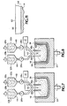
- the method shown in FIGS. 5-6 is for making the crucible embodiment shown in FIGS. 1-2.
- the bulk grain hopper 22a To form the bulk grain layer 36, the bulk grain hopper 22a, flow regulating valve 26a and feed tube 24 are used.
- bulk silica grain 30 is introduced into a mold 20 to form the bulk grain layer 36.
- the bulk silica grain 30 is preferably pure quartz grain. Hopper stirring blade 28a aids the uniform flow of grain from the hopper 22a.
- a scraper 32 shaped to conform to the inner surface of the mold, is generally used to shape the introduced bulk silica grain. In this manner, the bulk grain layer 36 can be formed to a selected thickness.
- FIG. 6 Fusion of formed silica grain is shown in FIG. 6.
- An electrode assembly comprising a power source 37 and electrodes 38a,38b, is positioned partially within the interior cavity of the rotating mold 20.
- An electric arc is produced between electrodes 38a, 38b by supplying 250-350 V and approximately 1800 A direct current.
- a region of heat 42 is thereby generated within the mold interior. This heat 42 serves to fuse formed bulk grain layer 36 in the mold.
- Fusion proceeds through the formed grain from proximal to distal, relative to electrodes 38a,38b.
- the mechanism of progressive fusion through the silica grain layer according to this technique is known to those skilled in the art, for example, as disclosed in U.S. Patent Nos. 4,935,046 and 4,956,208 both to Uchikawa et al.
- inner silica grain 44 is poured from the inner silica grain hopper 22b through feed tube 40.
- Inner grain flow regulating valve 26b can be utilized to control the rate at which inner layer grain 44 is introduced into the region of heat 42.
- Hopper stirring blade 28b also aids the homogeneity and uniform flow of grain from the hopper 22b.
- the arc produced between the electrodes creates a very strong plasma field, propelling the partially melted inner silica grain 44 outward, enabling it to be deposited on the sides and bottom of the crucible inner surface.
- the inner grain 44 passes through the heated region 42, is at least partially melted by the arc flame therein, and is deposited on the surface of the bulk layer, which is the fused bulk grain layer 36.
- the introduced inner grain 44 is fused to the bulk layer to form an inner layer 16. Molten inner grain thereby is continuously deposited and fused over a period of time of inner layer formation.
- the inner layer 16 thus formed is essentially transparent and bubble-free.
- the thickness of fused inner layer is controlled by the introduction rate of inner silica grain and by the period of inner grain supply during fusion.
- Inner silica grain 44 consists essentially of silica grain, such as natural silica grain washed to remove contaminants, doped with barium. Alternatively, synthetic silica grain doped with barium can be used.
- the bulk layer is numbered as 36 representing bulk grain layer for convenience.
- this layer is actually a dynamic combination of fused bulk layer 14 and unfused bulk grain layer 36.
- a method for making a crucible having both an inner layer and a transition layer comprises the steps shown in FIGS. 5 and 7-8.
- the electrode assembly After formation of a bulk grain layer 36, the electrode assembly is positioned within the crucible interior cavity and a transition layer 18 is fused to the partially fused bulk layer 14, in a manner similar to deposition of the inner layer as in FIG.6.
- Transition grain 48 is supplied from the transition grain hopper 22c through flow controlling valve 26c.
- Hopper stirring blade 28c can be employed similarly to stirring blade 28a.
- the hopper assembly After deposition of the transition layer 18, the hopper assembly ceases introduction of transition silica grain 48 by closing transition grain flow regulating valve 26c. Inner grain 44, contained in hopper 22b, is then introduced via opening of flow regulating valve 26b. Inner grain 44 is introduced into the region of heat 42, is at least partially melted and deposited as inner layer 16 on transition layer 18.
- transition layer 18 and inner layer 16 are controlled with the help of flow controlling valves 26c,26b, respectively.
- the transition layer 18 is a transparent layer prepared between the inner layer 16 (typically also transparent) and the translucent bulk layer 14.
- the barium-doped grain can be put on any kind of transparent transition layer.
- the transition layer 18 can be a pure silica layer, an aluminum-doped layer, or a layer doped with another dopant.
- the barium-doped inner layer is deposited on a transparent layer of synthetic silica glass or pure silica glass made from purified natural quartz.
- a similar method is used to construct the crucible shown in FIG. 4.
- An outer grain layer is first formed in a rotating mold 20, as shown in FIG. 9. the thickness of the outer grain layer is controlled using a scraper 47.
- An outer grain hopper 22d communicates via a feed tube 24 with the interior of the mold 20.
- the feed tube 24 can employ a valve 26d to regulate the flow of outer silica grain 46 from the hopper 22d to the interior of the mold.
- Outer silica grain is flowed thereby into the rotating mold. Rotation of the crucible mold provides sufficient centrifugal force to retain the poured outer silica grain on the inner side surface of the mold as outer grain layer 49
- outer layer it is preferable that it be doped with aluminum rather than barium:
- One reason is that disposal of unfused doped outer silica grain is more convenient if the dopant is aluminum, for environmental concerns.
- Unfused bulk silica grain 30 (and unfused outer grain, if present) is left on the exterior of the crucible. Thus, a rough, bubble-containing outermost surface results. Unfused grain is disposed of in subsequent processing of the crucible, typically by sand-blasting and rinsing with water.
- Barium is chosen as the doping element, because a small amount of barium can crystallize the silica glass and if it is dissolved in the silicon melt it will not be transferred to the silicon crystal in large amount.
- the inner silica grain 44 contains barium via doping.
- Barium can alternatively be introduced contemporaneously with essentially pure silica grain, i.e., a barium-containing compound can be mixed with essentially pure inner silica grain.
- barium carbonate (BaCO 3 ) can be placed in the inner grain hopper 22b.
- a mixing blade 28b can be used to ensure uniform distribution of the barium-containing compound in the inner silica grain.
- the inner silica grain and barium carbonate mixture then can be flowed into the region of heat as described above.
- the essentially pure silica grain can be either undoped natural or synthetic silica grain.
- the barium-containing compound can be separately introduced into the heated region contemporaneous with inner silica grain introduction.
- a separate barium compound hopper can be provided, containing, for example, BaCO 3 .
- the valves controlling the inner grain hopper and the barium compound hopper can both be opened, so as to flow concurrently.
- the transition silica grain can also be employed as the inner silica grain.
- the transition silica grain can be flowed to form a transition layer as described above. The transition hopper flow is stopped, and then both transition silica grain and barium compound are flowed simultaneously into the heated region.
- the transition layer can be formed as originally described, and then the barium compound flow can be initiated contemporaneous with the still-flowing transition silica grain, to form thereby the inner layer having a barium component therein.
- the barium compound flow rate can be variable, such that a barium gradient from the inner surface to the transition layer is formed.
- the barium-containing compound can be in liquid form, e.g., an aqueous solution of barium hydroxide (Ba(OH) 2 ) or barium chloride (BaCl 2 ).
- the liquid solution can be introduced into the inner silica grain 44 prior to or contemporaneous with introduction of the inner silica grain into the heated region, or the liquid solution can be introduced directly into the heated region.
- the latter introduction can be accomplished by an injecting or misting device.
- the injecting device generally should be positioned adjacent the end of the flow tube proximate the heated region.
- the inner layer in the crucible wall is doped with barium in the range of about 5-150 wtppm, and most preferably between 15-75 wtppm.
- the inner layer preferably is free of bubbles, as bubbles entrapped within the inner layer may generate fracture-inducing particles as the layer crystallizes. Such particles can dissociate or break away from the inner surface as the bubble expands and as the inner surface erodes or dissolves into the silicon melt. Loose particles can cause loss of the single-crystal structure in the silicon ingot.
- the method disclosed above dopes a crucible inner layer with barium, rather than coating the interior surface of the crucible with a barium compound.
- This improved method i.e., barium doping, has several merits over conventional coating methods.
- the present method enables the concentration of barium in the inner layer to be finely controlled.
- the inner layer silica grain is doped with barium prior to its introduction into the mold and fusion.
- the amount of barium contained in the barium-doped grain can be determined in advance by analysis.
- the dopant level in the inner layer can thereby be fine-tuned, for example, by mixing doped silica grain and pure silica grain in the hopper.
- the doped inner layer thickness can also be precisely controlled by changing inner silica grain flow rate or flow time. No loss of the barium element was observed, e.g., loss due to sublimation. Substantially all of the introduced dopant was found to be fixed within the inner layer.
- the thickness of the crystallization in the layer is controlled. Only the region doped with barium crystallizes; regions not doped with barium do not crystallize during a typical CZ-process operation. This characteristic gives a crucible designer greater freedom to tailor the crucible to the needs of the process in which it will be employed.
- the crucibles can be machined to dimensions, cleaned or etched, and handled with the same procedures as for normal pure silica crucibles; no additional post-manufacture processing or special handling of the crucible is required.
- unfused grain remaining on the outside of a conventional crucible is cleaned by sand-blasting, followed by rinsing with water. After cutting the crucible to specified dimensions, it is cleaned by etching with dilute hydrofluoric acid and rinsing with pure water.
- the crucible is dried in a clean air bath, then bagged and boxed for shipment.
- a user typically unpacks the crucible and again cleans it before use (by rinsing with water or wiping with alcohol or any other methods as commonly used for pure silica glass crucibles).
- a crucible constructed according to the present disclosure can be handled as described above.
- the present crucible suppresses the generation of rosettes, which structures are the initial cause of the roughening of the inner surface. Rosette suppression is accomplished by crystallization of the inner surface of a crucible wall prior to full melt-down of the silicon charge in a CZ process.
- the present disclosure employs barium doping to provide a mode for lengthening the useful life of a crucible suitable for use in a CZ-process.
- Generation of rosettes can be suppressed by crystallizing the inner layer 16 of a crucible wall 14 (FIG. 11) prior to silicon charge melt-down in a CZ-process.
- the inner layer undergoes a phase transformation from fused silica glass to crystobalite 56, so that the inner surface 62 retains its smooth surface finish throughout.
- the inner surface 62 of the crucible is covered with crystobalite 56 before melt-down of the charged silicon.
- Rosettes are not formed by a reaction between the silicon melt and crystalline silica. Because a rosette is not generated, a rough surface area does not appear and the inner surface remains smooth.
- Some silicon ingot manufacturers perform sequential silicon crystal "pulls" using the same crucible. In these uses, a subset of the crucible side portion is alternately covered by the melt, exposed to atmosphere as the melt level drops, then covered again as silicon charge is added to begin another ingot pull.
- the inner surface of a crucible thus used is subjected to high stress for a longer time period, making more important the inner surface textural integrity.
- the barium doping level in the inner layer and the thickness of the inner layer has an effect on the rapidity of crystallization in the layer. Therefore, the depth and amount of barium doping in the inner layer is important to achieve a fully crystallized inner layer.
- crucibles A, B, C, D and E were manufactured according to the present disclosure.
- crucible P was constructed according to the prior art. These crucibles have similar dimensions, e.g., nominal diameters of 24 inches.
- Barium doping levels were varied from 10-50 wtppm for crucibles A-E, and inner layer thickness was also varied from 0.2-0.8 mm.
- the inner layer 16 of Crucibles A-E were made using a barium-doped inner silica grain.
- Crucibles A-D were made according to the above-disclosed method, with the inner layer thicknesses and doping levels as follows: crucible A, 0.8mm layer at 10 wtppm; crucible B, 0.5mm layer at 25 wtppm; crucible C, 0.2mm layer at 50 wtppm; and crucible D, 1.0mm layer at 50 wtppm.
- Crucible E is a comparative embodiment, made with an inner layer of 0.1mm layer at 50 wtppm.
- the prior art crucible P was of 24-inch diameter.
- a 1.0mm-thick inner layer was formed in its interior using pure natural silica grain instead of barium-doped inner silica grain.
- This natural silica grain contained trace amounts ( ⁇ 0.1 wtppm) of barium and roughly 8 wtppm aluminum.
- Crucibles A-E and P were used in a 120-hour CZ-process, i.e., 120 hours at the chosen high temperature including melting of the silicon charge. The results of these processes are described below.
- Crucibles A-E and P were subjected to a 120-hour CZ-process, after which the inner layer was examined.
- the smooth inner surface of crucibles A-D were found to consist essentially of crystobalite, with no rosette pattern evident.
- the crucible inner surface presented a smooth finish.
- the 200-mm diameter silicon crystals made using crucibles A-D were also assessed. Dislocations were not observed in the silicon ingots.
- Prior art crucible P was started in a similar 120-hour CZ-process. However, at about 80 hours into the process, the nascent silicon ingot incurred a grain boundary flaw that disrupted its crystal structure. This flaw forced termination of the CZ-process and rendered the silicon crystal unsuitable for use in semiconductor manufacture.
Landscapes
- Chemical & Material Sciences (AREA)
- Engineering & Computer Science (AREA)
- Materials Engineering (AREA)
- Organic Chemistry (AREA)
- Crystallography & Structural Chemistry (AREA)
- Metallurgy (AREA)
- Manufacturing & Machinery (AREA)
- Crystals, And After-Treatments Of Crystals (AREA)
Abstract
Description
- FIG. 1
- is a cross-sectional view of one embodiment of a silica glass crucible constructed according to the present disclosure.
- FIG. 2
- is an enlarged, partial cross-sectional view of the wall of the silica glass crucible shown in FIG. 1.
- FIG. 3
- is an enlarged, partial cross-sectional view of the wall of a second embodiment of a silica glass crucible constructed according to the present disclosure.
- FIG. 4
- is an enlarged, partial cross-sectional view of the wall of a third embodiment of a silica glass crucible constructed according to the present disclosure.
- FIGS. 5 - 6
- are diagrams showing a method for making the silica glass crucible shown in FIGS. 1-2.
- FIGS. 7- 8
- are diagrams showing a method for making the second embodiment silica glass crucible shown in FIG. 3.
- FIG. 9
- is a diagram showing the initial step of forming an outer layer, to form the third embodiment silica glass crucible of FIG. 4.
- FIGS. 10A-10C
- are plan views of a prior art crucible inner surface at various stages of a CZ run.
- FIG. 11
- is an enlarged cross-sectional view of the portion of a crucible constructed according to the present disclosure, in which the inner layer is crystallized.
Claims (38)
- A crucible comprising:a wall having a side portion and a bottom portion thereby defining an interior cavity, said wall comprising: a bulk layer; and an inner doped with barium.
- The crucible of claim 1, wherein the inner layer is in the range of 0.2-1.2mm deep.
- The crucible of claim 1 or claim 2, wherein the inner layer is doped with barium in the range of about 5-150 wtppm.
- The crucible of claim 3, wherein the inner layer is doped with barium in the range of about 15-75 wtppm.
- The crucible of one of the preceding claims, the wall further comprising a metal-doped outer layer formed on an outer portion of said wall.
- The crucible of claim 5, wherein the outer layer is substantially an outer layer of the side portion.
- The crucible of claim 5 or claim 6, wherein the outer layer is about 0.5 mm-2.5 mm deep.
- The crucible of one of the claims 5 to 7, wherein the outer layer is doped with aluminum in the range of about 100-500 wtppm.
- The crucible of one of the preceding claims, wherein said inner layer is at least partially crystallized.
- The crucible of one of the preceding claims, wherein said inner layer is adapted to substantially completely crystallize prior to full melt-down of a silicon charge in a Czochralski process.
- The crucible of one of the preceding claims, wherein the wall further comprising a transition layer formed between the inner layer and the bulk layer.
- The crucible of claim 11, wherein the transition layer is free of barium doping.
- The crucible of one of the preceding claims 11 or 12, wherein the transition layer consists essentially of natural silica glass.
- The crucible of one of the preceding claims 11 to 13, wherein the transition layer consists essentially of synthetic silica glass.
- The crucible of one of the preceding claims 11 to 14, wherein the transition layer is doped with a metal.
- The crucible of claim 15, wherein the metal is aluminum.
- A method for making a silica glass crucible, comprising:forming a bulk grain layer on an interior surface of a rotating crucible mold, said bulk grain layer having a bottom portion, a side portion and a bulk grain layer interior surface;generating a region of heat in the interior of the mold, wherein the region of heat at least partially fuses said bulk grain layer to form a bulk layer; anddepositing a barium-containing inner layer on the bulk grain layer interior surface.
- The method of claim 17, wherein forming a bulk grain layer comprises introducing into the rotating crucible mold bulk silica grain.
- The method of claim 18, wherein bulk silica grain consists essentially of quartz grain.
- The method of one of the claims 17 to 19, wherein a selected thickness of the inner layer is in the range of 0.2-1.0mm.
- The method of one of the claims 17 to 21, wherein depositing a barium-containing inner layer comprises introducing into said mold inner silica grain doped with barium, wherein the region of heat at least partially melts said inner silica grain and fuses said at least partially molten inner silica grain to the bulk layer.
- The method of claim 21, wherein the inner silica grain is doped with barium in the range of 5-150 wtppm.
- The method of claim 21, wherein the inner silica grain is doped with barium in the range of 15-75 wtppm.
- The method of claim 17, wherein depositing a barium-containing inner layer comprises introducing into said mold inner silica grain and barium, and wherein the region of heat at least partially melts said inner silica grain and fuses said at least partially molten inner silica grain to the bulk layer.
- The method of claim 24, wherein the inner silica grain consists essentially of natural silica grain.
- The method of claim 24, wherein the inner silica grain consists essentially of synthetic silica grain.
- The method of claim 24, wherein the barium is a solid compound admixed with the inner silica grain.
- The method of claim 27, wherein the solid barium compound is admixed with the inner silica grain prior to introducing into said mold inner silica grain and barium.
- The method of one of the preceding claims 17 to 28, further comprising, prior to forming a bulk grain layer:forming an outer grain layer on an interior surface of a rotating crucible mold, wherein the region of heat at least partially fuses said outer grain layer to form an outer layer.
- The method of claim 29, wherein the outer layer is formed substantially on the side portion.
- The method of claim 29 or claim 30, wherein forming an outer grain layer comprises introducing into the rotating crucible mold outer silica grain.
- The method of claim 31, wherein the outer silica grain is doped with aluminum in the range of 100-500 wtppm.
- The method of one of the preceding claims 17 to 28, further comprising, depositing a transition layer on the bulk grain layer and depositing the barium-containing inner layer on the transition layer.
- The method of claim 33, wherein depositing a transition layer comprises introducing into a rotating crucible mold transition silica grain, wherein the region of heat at least partially melts said transition silica grain and fuses said at least partially molten transition silica grain to the bulk layer to form the transition layer.
- The method of claim 34, wherein the transition silica grain consists essentially of natural silica grain.
- The method of claim 34, wherein the transition silica grain consists essentially of synthetic silica grain.
- The method of claim 34, wherein the transition silica grain is doped with a metal.
- The method of claim 37, wherein the metal is aluminum.
Applications Claiming Priority (2)
| Application Number | Priority Date | Filing Date | Title |
|---|---|---|---|
| US10/021,631 US6641663B2 (en) | 2001-12-12 | 2001-12-12 | Silica crucible with inner layer crystallizer and method |
| US21631 | 2001-12-12 |
Publications (2)
| Publication Number | Publication Date |
|---|---|
| EP1319736A1 true EP1319736A1 (en) | 2003-06-18 |
| EP1319736B1 EP1319736B1 (en) | 2006-05-10 |
Family
ID=21805284
Family Applications (1)
| Application Number | Title | Priority Date | Filing Date |
|---|---|---|---|
| EP02027195A Expired - Lifetime EP1319736B1 (en) | 2001-12-12 | 2002-12-05 | Silica crucible with inner layer crystallizer and method for its manufacturing |
Country Status (3)
| Country | Link |
|---|---|
| US (2) | US6641663B2 (en) |
| EP (1) | EP1319736B1 (en) |
| DE (1) | DE60211289T2 (en) |
Cited By (8)
| Publication number | Priority date | Publication date | Assignee | Title |
|---|---|---|---|---|
| WO2005056886A1 (en) * | 2003-12-03 | 2005-06-23 | General Electric Company | Quartz crucibles having reduced bubble content and method of making thereof |
| US7299658B2 (en) | 2003-05-30 | 2007-11-27 | Heraeus Quarzglas Gmbh & Co. K.G. | Quartz glass crucible for the pulling up of silicon single crystal |
| RU2328562C1 (en) * | 2006-11-14 | 2008-07-10 | Открытое акционерное общество "Подольский химико-металлургический завод" | Method of formation of protective coat on inside surface of quartz crucible |
| EP1375702A3 (en) * | 2002-06-18 | 2008-12-24 | Heraeus Quarzglas GmbH & Co. KG | Doped silica glass crucible for making a silicon ingot |
| US7686887B2 (en) | 2002-07-31 | 2010-03-30 | Heraeus Quarzglas Gmbh & Co. Kg | Quartz glass crucible for pulling up silicon single crystal and method for producing the same |
| US8277559B2 (en) | 2003-05-01 | 2012-10-02 | Heraeus Quarzglas Gmbh & Co. Kg | Quartz glass crucible for pulling up silicon single crystal and method for manufacture thereof |
| EP2436658A4 (en) * | 2009-05-26 | 2015-04-22 | Shinetsu Quartz Prod | SILICA CONTAINER AND METHOD FOR PRODUCING SAME |
| US10308541B2 (en) | 2014-11-13 | 2019-06-04 | Gerresheimer Glas Gmbh | Glass forming machine particle filter, a plunger unit, a blow head, a blow head support and a glass forming machine adapted to or comprising said filter |
Families Citing this family (35)
| Publication number | Priority date | Publication date | Assignee | Title |
|---|---|---|---|---|
| US7118789B2 (en) * | 2001-07-16 | 2006-10-10 | Heraeus Shin-Etsu America | Silica glass crucible |
| US6712901B2 (en) * | 2001-10-16 | 2004-03-30 | Japan Super Quartz Corporation | Surface modification process of quartz glass crucible |
| DE10156137B4 (en) * | 2001-11-15 | 2004-08-19 | Wacker-Chemie Gmbh | Process for producing a silica glass crucible with crystalline areas from a porous silica glass green body |
| US20030183161A1 (en) | 2002-03-29 | 2003-10-02 | Japan Super Quartz Corporation | Surface modified quartz glass crucible and its modification process |
| JP4339003B2 (en) * | 2003-04-02 | 2009-10-07 | ジャパンスーパークォーツ株式会社 | Method for producing quartz glass crucible |
| US7497907B2 (en) * | 2004-07-23 | 2009-03-03 | Memc Electronic Materials, Inc. | Partially devitrified crucible |
| US7562858B2 (en) * | 2005-03-16 | 2009-07-21 | Diamond Innovations, Inc. | Wear and texture coatings for components used in manufacturing glass light bulbs |
| US7383696B2 (en) * | 2005-09-08 | 2008-06-10 | Heraeus Shin-Etsu America, Inc. | Silica glass crucible with bubble-free and reduced bubble growth wall |
| US7427327B2 (en) * | 2005-09-08 | 2008-09-23 | Heraeus Shin-Etsu America, Inc. | Silica glass crucible with barium-doped inner wall |
| US20070084400A1 (en) * | 2005-10-19 | 2007-04-19 | General Electric Company | Quartz glass crucible and method for treating surface of quartz glass crucible |
| US7556764B2 (en) * | 2005-11-09 | 2009-07-07 | Heraeus Shin-Etsu America, Inc. | Silica vessel with nozzle and method of making |
| TW200730672A (en) * | 2005-11-29 | 2007-08-16 | Japan Super Quartz Corp | Quartz glass crucible, method of producing the same, and application thereof |
| US7837955B2 (en) * | 2006-03-08 | 2010-11-23 | Unimin Corporation | Continuous reactor system for anoxic purification |
| TWI408259B (en) * | 2006-09-28 | 2013-09-11 | Shinetsu Quartz Prod | Silica glass crucible with barium-doped inner wall |
| US7716948B2 (en) * | 2006-12-18 | 2010-05-18 | Heraeus Shin-Etsu America, Inc. | Crucible having a doped upper wall portion and method for making the same |
| JP5229778B2 (en) * | 2007-09-28 | 2013-07-03 | 株式会社Sumco | Method for producing quartz glass crucible for pulling silicon single crystal |
| US8272234B2 (en) * | 2008-12-19 | 2012-09-25 | Heraeus Shin-Etsu America, Inc. | Silica crucible with pure and bubble free inner crucible layer and method of making the same |
| US20120006254A1 (en) * | 2009-02-10 | 2012-01-12 | Masaru Fujishiro | Quartz glass crucible for pulling single-crystal silicon and process for producing single-crystal silicon |
| US9003832B2 (en) * | 2009-11-20 | 2015-04-14 | Heraeus Shin-Etsu America, Inc. | Method of making a silica crucible in a controlled atmosphere |
| CN102453956B (en) * | 2010-10-27 | 2016-03-23 | 杭州先进石英材料有限公司 | A kind of quartz glass crucibles and preparation method thereof |
| JP5605902B2 (en) * | 2010-12-01 | 2014-10-15 | 株式会社Sumco | Method for producing silica glass crucible, silica glass crucible |
| JP5500689B2 (en) * | 2010-12-03 | 2014-05-21 | 株式会社Sumco | Silica glass crucible |
| JP5773382B2 (en) * | 2010-12-29 | 2015-09-02 | 株式会社Sumco | Silica glass crucible and method for producing the same |
| JP4854814B1 (en) | 2011-04-28 | 2012-01-18 | Ftb研究所株式会社 | Method for coating quartz crucible for silicon crystal growth and quartz crucible for silicon crystal growth |
| JP5509188B2 (en) * | 2011-12-26 | 2014-06-04 | ジルトロニック アクチエンゲゼルシャフト | Method for producing single crystal silicon |
| JP5509189B2 (en) * | 2011-12-26 | 2014-06-04 | ジルトロニック アクチエンゲゼルシャフト | Method for producing single crystal silicon |
| US20140352605A1 (en) * | 2013-05-31 | 2014-12-04 | Heraeus Shin-Etsu America, Inc. | Method for making barium-doped crucible and crucible made thereby |
| CN104389014B (en) * | 2014-12-02 | 2017-04-05 | 江苏科技大学 | A kind of silica crucible for crystal growth and preparation method thereof |
| CN104651932B (en) * | 2015-03-17 | 2017-11-07 | 江西中昱新材料科技有限公司 | A kind of polycrystalline quartz ceramic crucible and preparation method thereof |
| CN109563639B (en) | 2016-09-13 | 2021-10-26 | 胜高股份有限公司 | Quartz glass crucible and method for producing same |
| JP7341017B2 (en) * | 2019-09-30 | 2023-09-08 | 信越石英株式会社 | Method for manufacturing heat reflective member and glass member with heat reflective layer |
| CN110541193A (en) * | 2019-10-11 | 2019-12-06 | 内蒙古中环协鑫光伏材料有限公司 | Quartz crucible and preparation method thereof |
| CN110552057A (en) * | 2019-10-11 | 2019-12-10 | 内蒙古中环协鑫光伏材料有限公司 | A new type of quartz crucible and a method for improving the life of the tail of a single crystal silicon rod |
| CN110552056A (en) * | 2019-10-11 | 2019-12-10 | 内蒙古中环协鑫光伏材料有限公司 | Method for improving Czochralski single crystal formation |
| US11873574B2 (en) | 2019-12-13 | 2024-01-16 | Globalwafers Co., Ltd. | Systems and methods for production of silicon using a horizontal magnetic field |
Citations (8)
| Publication number | Priority date | Publication date | Assignee | Title |
|---|---|---|---|---|
| US4935046A (en) * | 1987-12-03 | 1990-06-19 | Shin-Etsu Handotai Company, Limited | Manufacture of a quartz glass vessel for the growth of single crystal semiconductor |
| JPH082932A (en) * | 1994-06-20 | 1996-01-09 | Shinetsu Quartz Prod Co Ltd | Quartz glass crucible and method of manufacturing the same |
| EP0753605A1 (en) * | 1995-06-14 | 1997-01-15 | MEMC Electronic Materials, Inc. | Methods for improving zero dislocation yield of single crystals |
| US5885071A (en) * | 1996-03-18 | 1999-03-23 | Watanabe; Hiroyuki | Quartz glass crucible for pulling single crystal |
| EP0911429A1 (en) * | 1997-09-30 | 1999-04-28 | Heraeus Quarzglas GmbH | Quartz glass crucible for producing silicon single crystal and method for producing the crucible |
| US5976247A (en) * | 1995-06-14 | 1999-11-02 | Memc Electronic Materials, Inc. | Surface-treated crucibles for improved zero dislocation performance |
| US20010032580A1 (en) * | 1999-03-15 | 2001-10-25 | Phillips Richard J. | Barium doping of molten silicon for use in crystal growing process |
| US20020139143A1 (en) * | 2001-03-08 | 2002-10-03 | Gabriele Korus | Method of producing a quartz glass crucible |
Family Cites Families (8)
| Publication number | Priority date | Publication date | Assignee | Title |
|---|---|---|---|---|
| US4637571A (en) | 1985-09-03 | 1987-01-20 | The United States Of America As Represented By The Secretary Of The Army | Electronic image stabilization |
| JPH01126238A (en) | 1987-11-09 | 1989-05-18 | Shinetsu Sekiei Kk | Quartz glass member |
| JP3268049B2 (en) | 1993-01-26 | 2002-03-25 | 東芝セラミックス株式会社 | Quartz glass material and its manufacturing method |
| JP3040315B2 (en) | 1994-08-03 | 2000-05-15 | 信越化学工業株式会社 | High viscosity synthetic quartz glass member and method for producing the same |
| JP3621282B2 (en) | 1999-02-25 | 2005-02-16 | 東芝セラミックス株式会社 | Quartz glass crucible and method for producing the same |
| US6350312B1 (en) | 1999-03-15 | 2002-02-26 | Memc Electronic Materials, Inc. | Strontium doping of molten silicon for use in crystal growing process |
| WO2002040732A1 (en) | 2000-11-15 | 2002-05-23 | G.T. Equipment Technologies Inc. | A protective layer for quartz crucibles used for silicon crystallization |
| US6875515B2 (en) * | 2002-05-10 | 2005-04-05 | General Electric Company | Fused quartz article having controlled devitrification |
-
2001
- 2001-12-12 US US10/021,631 patent/US6641663B2/en not_active Expired - Lifetime
-
2002
- 2002-12-05 DE DE60211289T patent/DE60211289T2/en not_active Expired - Lifetime
- 2002-12-05 EP EP02027195A patent/EP1319736B1/en not_active Expired - Lifetime
-
2003
- 2003-09-03 US US10/654,805 patent/US20040040497A1/en not_active Abandoned
Patent Citations (10)
| Publication number | Priority date | Publication date | Assignee | Title |
|---|---|---|---|---|
| US4935046A (en) * | 1987-12-03 | 1990-06-19 | Shin-Etsu Handotai Company, Limited | Manufacture of a quartz glass vessel for the growth of single crystal semiconductor |
| US4956208A (en) * | 1987-12-03 | 1990-09-11 | Shin-Etsu Handotai Co., Ltd. | Manufacture of a quartz glass vessel for the growth of single crystal semiconductor |
| JPH082932A (en) * | 1994-06-20 | 1996-01-09 | Shinetsu Quartz Prod Co Ltd | Quartz glass crucible and method of manufacturing the same |
| EP0753605A1 (en) * | 1995-06-14 | 1997-01-15 | MEMC Electronic Materials, Inc. | Methods for improving zero dislocation yield of single crystals |
| US5976247A (en) * | 1995-06-14 | 1999-11-02 | Memc Electronic Materials, Inc. | Surface-treated crucibles for improved zero dislocation performance |
| US5885071A (en) * | 1996-03-18 | 1999-03-23 | Watanabe; Hiroyuki | Quartz glass crucible for pulling single crystal |
| EP0911429A1 (en) * | 1997-09-30 | 1999-04-28 | Heraeus Quarzglas GmbH | Quartz glass crucible for producing silicon single crystal and method for producing the crucible |
| US20010032580A1 (en) * | 1999-03-15 | 2001-10-25 | Phillips Richard J. | Barium doping of molten silicon for use in crystal growing process |
| US6319313B1 (en) * | 1999-03-15 | 2001-11-20 | Memc Electronic Materials, Inc. | Barium doping of molten silicon for use in crystal growing process |
| US20020139143A1 (en) * | 2001-03-08 | 2002-10-03 | Gabriele Korus | Method of producing a quartz glass crucible |
Non-Patent Citations (1)
| Title |
|---|
| PATENT ABSTRACTS OF JAPAN vol. 1996, no. 05 31 May 1996 (1996-05-31) * |
Cited By (8)
| Publication number | Priority date | Publication date | Assignee | Title |
|---|---|---|---|---|
| EP1375702A3 (en) * | 2002-06-18 | 2008-12-24 | Heraeus Quarzglas GmbH & Co. KG | Doped silica glass crucible for making a silicon ingot |
| US7686887B2 (en) | 2002-07-31 | 2010-03-30 | Heraeus Quarzglas Gmbh & Co. Kg | Quartz glass crucible for pulling up silicon single crystal and method for producing the same |
| US8277559B2 (en) | 2003-05-01 | 2012-10-02 | Heraeus Quarzglas Gmbh & Co. Kg | Quartz glass crucible for pulling up silicon single crystal and method for manufacture thereof |
| US7299658B2 (en) | 2003-05-30 | 2007-11-27 | Heraeus Quarzglas Gmbh & Co. K.G. | Quartz glass crucible for the pulling up of silicon single crystal |
| WO2005056886A1 (en) * | 2003-12-03 | 2005-06-23 | General Electric Company | Quartz crucibles having reduced bubble content and method of making thereof |
| RU2328562C1 (en) * | 2006-11-14 | 2008-07-10 | Открытое акционерное общество "Подольский химико-металлургический завод" | Method of formation of protective coat on inside surface of quartz crucible |
| EP2436658A4 (en) * | 2009-05-26 | 2015-04-22 | Shinetsu Quartz Prod | SILICA CONTAINER AND METHOD FOR PRODUCING SAME |
| US10308541B2 (en) | 2014-11-13 | 2019-06-04 | Gerresheimer Glas Gmbh | Glass forming machine particle filter, a plunger unit, a blow head, a blow head support and a glass forming machine adapted to or comprising said filter |
Also Published As
| Publication number | Publication date |
|---|---|
| US6641663B2 (en) | 2003-11-04 |
| US20040040497A1 (en) | 2004-03-04 |
| US20030106491A1 (en) | 2003-06-12 |
| EP1319736B1 (en) | 2006-05-10 |
| DE60211289D1 (en) | 2006-06-14 |
| DE60211289T2 (en) | 2007-03-29 |
Similar Documents
| Publication | Publication Date | Title |
|---|---|---|
| EP1319736B1 (en) | Silica crucible with inner layer crystallizer and method for its manufacturing | |
| US7118789B2 (en) | Silica glass crucible | |
| EP1375702B1 (en) | Doped silica glass crucible for making a silicon ingot | |
| KR20030007210A (en) | Doped silica glass crucible for making a silicon ingot | |
| JP4948504B2 (en) | Silicon single crystal pulling method | |
| US6106610A (en) | Quartz glass crucible for producing silicone single crystal and method for producing the crucible | |
| JP7820140B2 (en) | Quartz glass crucible | |
| US8562739B2 (en) | Silica glass crucible for pulling up silicon single crystal and method for manufacturing thereof | |
| KR101104673B1 (en) | High Purity Quartz Glass Crucible for Large Diameter Silicon Single Crystal Ingot Impression | |
| JP2000247778A (en) | Quartz glass crucible, method for producing the same, and method for pulling silicon single crystal using the same | |
| WO2000059837A1 (en) | Method for manufacturing quartz glass crucible | |
| JP4548682B2 (en) | Manufacturing method of quartz glass crucible | |
| EP2460778B1 (en) | Method of manufacturing vitreous silica crucible | |
| JP4233059B2 (en) | Silica glass crucible for pulling silicon single crystal and method for producing the same | |
| JP2840195B2 (en) | Method for producing quartz glass crucible for single crystal pulling | |
| JPS59213697A (en) | Pulling device for single crystal semiconductor | |
| JPH11292694A (en) | Quartz crucible for pulling silicon single crystal | |
| JP3983054B2 (en) | Quartz glass crucible for pulling silicon single crystal and method for producing the same | |
| JP4601437B2 (en) | Quartz glass crucible with inner surface semi-crystallized and manufacturing method thereof | |
| JPH1149597A (en) | Quartz crucible for pulling silicon single crystal | |
| JP3798907B2 (en) | Quartz glass crucible for producing silicon single crystal and method for producing the same | |
| JP2006213556A (en) | Quartz glass crucible for pulling silicon single crystal and production method therefor, and method for taking out the crucible | |
| JP2000072589A (en) | Quartz glass crucible for pulling silicon single crystal and method for producing the same | |
| JP7768072B2 (en) | Quartz glass crucible for pulling silicon single crystals and method for producing silicon single crystals using the same | |
| JP3026088B2 (en) | Quartz crucible for pulling silicon single crystal |
Legal Events
| Date | Code | Title | Description |
|---|---|---|---|
| PUAI | Public reference made under article 153(3) epc to a published international application that has entered the european phase |
Free format text: ORIGINAL CODE: 0009012 |
|
| AK | Designated contracting states |
Designated state(s): AT BE BG CH CY CZ DE DK EE ES FI FR GB GR IE IT LI LU MC NL PT SE SI SK TR |
|
| AX | Request for extension of the european patent |
Extension state: AL LT LV MK RO |
|
| 17P | Request for examination filed |
Effective date: 20030924 |
|
| AKX | Designation fees paid |
Designated state(s): DE FI FR GB IT |
|
| 17Q | First examination report despatched |
Effective date: 20040212 |
|
| GRAP | Despatch of communication of intention to grant a patent |
Free format text: ORIGINAL CODE: EPIDOSNIGR1 |
|
| GRAS | Grant fee paid |
Free format text: ORIGINAL CODE: EPIDOSNIGR3 |
|
| GRAA | (expected) grant |
Free format text: ORIGINAL CODE: 0009210 |
|
| AK | Designated contracting states |
Kind code of ref document: B1 Designated state(s): DE FI FR GB IT |
|
| PG25 | Lapsed in a contracting state [announced via postgrant information from national office to epo] |
Ref country code: IT Free format text: LAPSE BECAUSE OF FAILURE TO SUBMIT A TRANSLATION OF THE DESCRIPTION OR TO PAY THE FEE WITHIN THE PRE;WARNING: LAPSES OF ITALIAN PATENTS WITH EFFECTIVE DATE BEFORE 2007 MAY HAVE OCCURRED AT ANY TIME BEFORE 2007. THE CORRECT EFFECTIVE DATE MAY BE DIFFERENT FROM THE ONE RECORDED.SCRIBED TIME-LIMIT Effective date: 20060510 Ref country code: FI Free format text: LAPSE BECAUSE OF FAILURE TO SUBMIT A TRANSLATION OF THE DESCRIPTION OR TO PAY THE FEE WITHIN THE PRESCRIBED TIME-LIMIT Effective date: 20060510 |
|
| REG | Reference to a national code |
Ref country code: GB Ref legal event code: FG4D |
|
| REF | Corresponds to: |
Ref document number: 60211289 Country of ref document: DE Date of ref document: 20060614 Kind code of ref document: P |
|
| PLBE | No opposition filed within time limit |
Free format text: ORIGINAL CODE: 0009261 |
|
| STAA | Information on the status of an ep patent application or granted ep patent |
Free format text: STATUS: NO OPPOSITION FILED WITHIN TIME LIMIT |
|
| 26N | No opposition filed |
Effective date: 20070213 |
|
| EN | Fr: translation not filed | ||
| PG25 | Lapsed in a contracting state [announced via postgrant information from national office to epo] |
Ref country code: FR Free format text: LAPSE BECAUSE OF FAILURE TO SUBMIT A TRANSLATION OF THE DESCRIPTION OR TO PAY THE FEE WITHIN THE PRESCRIBED TIME-LIMIT Effective date: 20070309 |
|
| PG25 | Lapsed in a contracting state [announced via postgrant information from national office to epo] |
Ref country code: FR Free format text: LAPSE BECAUSE OF FAILURE TO SUBMIT A TRANSLATION OF THE DESCRIPTION OR TO PAY THE FEE WITHIN THE PRESCRIBED TIME-LIMIT Effective date: 20060510 |
|
| PGFP | Annual fee paid to national office [announced via postgrant information from national office to epo] |
Ref country code: GB Payment date: 20091218 Year of fee payment: 8 |
|
| GBPC | Gb: european patent ceased through non-payment of renewal fee |
Effective date: 20101205 |
|
| PG25 | Lapsed in a contracting state [announced via postgrant information from national office to epo] |
Ref country code: GB Free format text: LAPSE BECAUSE OF NON-PAYMENT OF DUE FEES Effective date: 20101205 |
|
| REG | Reference to a national code |
Ref country code: DE Ref legal event code: R082 Ref document number: 60211289 Country of ref document: DE Representative=s name: STAUDT, ARMIN, DIPL.-ING. (UNIV.), DE Ref country code: DE Ref legal event code: R081 Ref document number: 60211289 Country of ref document: DE Owner name: HERAEUS QUARZGLAS GMBH & CO. KG, DE Free format text: FORMER OWNERS: HERAEUS QUARZGLAS GMBH & CO. KG, 63450 HANAU, DE; HERAEUS SHIN-ETSU AMERICA, INC., CAMAS, WASH., US Ref country code: DE Ref legal event code: R081 Ref document number: 60211289 Country of ref document: DE Owner name: SHIN-ETSU QUARTZ PRODUCTS CO., LTD., JP Free format text: FORMER OWNERS: HERAEUS QUARZGLAS GMBH & CO. KG, 63450 HANAU, DE; HERAEUS SHIN-ETSU AMERICA, INC., CAMAS, WASH., US |
|
| PGFP | Annual fee paid to national office [announced via postgrant information from national office to epo] |
Ref country code: DE Payment date: 20201211 Year of fee payment: 19 |
|
| REG | Reference to a national code |
Ref country code: DE Ref legal event code: R119 Ref document number: 60211289 Country of ref document: DE |
|
| PG25 | Lapsed in a contracting state [announced via postgrant information from national office to epo] |
Ref country code: DE Free format text: LAPSE BECAUSE OF NON-PAYMENT OF DUE FEES Effective date: 20220701 |