EP1318710A2 - Abschirmung für Gehäuse, zur Abschirmung gegen elektromagnetische Strahlung - Google Patents
Abschirmung für Gehäuse, zur Abschirmung gegen elektromagnetische Strahlung Download PDFInfo
- Publication number
- EP1318710A2 EP1318710A2 EP02027132A EP02027132A EP1318710A2 EP 1318710 A2 EP1318710 A2 EP 1318710A2 EP 02027132 A EP02027132 A EP 02027132A EP 02027132 A EP02027132 A EP 02027132A EP 1318710 A2 EP1318710 A2 EP 1318710A2
- Authority
- EP
- European Patent Office
- Prior art keywords
- housing
- afb
- housing parts
- housing part
- shielding
- Prior art date
- Legal status (The legal status is an assumption and is not a legal conclusion. Google has not performed a legal analysis and makes no representation as to the accuracy of the status listed.)
- Granted
Links
Images

Classifications
-
- H—ELECTRICITY
- H05—ELECTRIC TECHNIQUES NOT OTHERWISE PROVIDED FOR
- H05K—PRINTED CIRCUITS; CASINGS OR CONSTRUCTIONAL DETAILS OF ELECTRIC APPARATUS; MANUFACTURE OF ASSEMBLAGES OF ELECTRICAL COMPONENTS
- H05K9/00—Screening of apparatus or components against electric or magnetic fields
- H05K9/0007—Casings
- H05K9/002—Casings with localised screening
- H05K9/0022—Casings with localised screening of components mounted on printed circuit boards [PCB]
- H05K9/0024—Shield cases mounted on a PCB, e.g. cans or caps or conformal shields
- H05K9/0032—Shield cases mounted on a PCB, e.g. cans or caps or conformal shields having multiple parts, e.g. frames mating with lids
- H05K9/0033—Shield cases mounted on a PCB, e.g. cans or caps or conformal shields having multiple parts, e.g. frames mating with lids disposed on both PCB faces
Definitions
- EMC electromagnetic compatibility
- the invention is therefore based on the object of the shielding or high-frequency tightness of electrically conductive Optimizing housings cost-effectively.
- the task is through a shield according to the features of the preamble of the claim 1 solved by its characteristic features.
- the shield for the housing consists of electrical conductive housing parts, at least one part the housing parts is arranged to overlap.
- the essential Aspect of the shielding according to the invention is that one of the overlapping housing parts each has an elongated, has edge-shaped elevation and the other housing part is designed with an elastic effect, that this elastic housing part in operative connection with the the housing part having the increase pressed on the increase becomes.
- the main advantage of the shielding according to the invention is in that by taking advantage of the elastic effect of housing parts to achieve good electronic shielding Circuits against electromagnetic interference no additional sealing elements such as EMC springs are required and consequently the number of attachment points reduced between housing parts and thereby the economic effort to realize an optimal Shielding can be minimized.
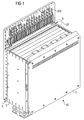
- FIG. 1 shows an electrically conductive housing in the form of a Subrack BT in which, for example, several circuit boards - not shown - with integrated, in high frequency range operated circuitry arranged are.
- This subrack BT can, for example in electrical switching devices for controlling Voice and data traffic in current telecommunication networks be used.
- the rack shown BT is composed of several side walls S, which for Part are formed from extruded profiles.
- FIG. 2 shows part of the subrack shown in FIG. 1 BT shown enlarged.
- the enlarged area and its viewing direction is shown in FIG 1 by the arrow A clarifies.
- 2 shows a section of the area of FIG Rear subrack cover overlap.
- This Area is a rear extruded profile Side part S arranged, which is an elongated or triangular running across the rear side part S.
- Raised K over which a rear subrack cover AD is spread during assembly.
- the rear subrack cover AD attached in the way to the rear side panel S - e.g. using a fastener B - that the rear Subrack cover AD over this elongated increase K is bent.
- the rear one Subrack cover AD with the increase K is over the entire length of the increase K - which extends across the rear Side part S extends - an electrical contact is made.
- the subrack is thus in the area of the active connection BT shielded against electromagnetic interference fields or sealed.
- FIG. 3 shows another in an enlarged view Design variant of the shield according to the invention.
- the The direction of viewing the enlarged area is shown in FIG. 1 indicated by arrow B.
- 3 shows an extruded profile designed side part S of the upper housing cover of the BT subrack.
- Extruded profile S with an elongated increase K provided.
- the increase K of the extruded profile S is in Active connection with an elastic sheet metal EB, which is part of an AFB connector panel of the subrack BT is.
- the extruded profile S is in the assembled Condition of the subrack BT in Art and way with the connector panel aperture AFB and the associated elastic sheet EB in operative connection that the elastic Sheet EB is bent around the increase K, so that the elastic sheet EB and the extruded profile S firmly into one another are wedged, and thus stable in electrically conductive Active connection.
- FIG. 3 is the elastic sheet EB of the connector panel AFB over an elongated area - in FIG 1 by a dashed circle UB clarifies - about the increase K bent, creating an elongated electrical Connection is established.
- the subrack BT against electromagnetic Interference fields shielded or sealed.
Landscapes
- Engineering & Computer Science (AREA)
- Microelectronics & Electronic Packaging (AREA)
- Shielding Devices Or Components To Electric Or Magnetic Fields (AREA)
Abstract
Description
- FIG 1
- ein zur Abschirmung von elektromagnetischen Störfeldern vorgesehenes, elektrisch leitendes Gehäuse in Form eines Baugruppenträgers,
- FIG 2 und 3
- jeweils Detaildarstellungen von unterschiedlichen Ausgestaltungsvarianten der erfindungsgemäßen Abschirmung.
Claims (4)
- Abschirmung für Gehäuse (BT), die aus elektrisch leitfähigen Gehäuseteilen (S) bestehen, zur Abschirmung gegen elektromagnetische Strahlung,
wobei zumindest ein Teil der Gehäuseteile (S, AD, EB, AFB) überlappend angeordnet ist,
dadurch gekennzeichnet, daß jeweils eines der überlappenden Gehäuseteile (S) eine länglich ausgebildete, kantenförmige Erhöhung (K) aufweist, daß das jeweils andere Gehäuseteil (AD, EB, AFB) derart mit einer elastischen Wirkung ausgestaltet ist, daß dieses elastische Gehäuseteil (AD, EB, AFB) in Wirkverbindung mit dem die Erhöhung (K) aufweisenden Gehäuseteil (S) auf die Erhöhung (K) gedrückt wird. - Abschirmung nach Anspruch 1,
dadurch gekennzeichnet, daß die elastische Wirkung des Gehäuseteils (AD, EB, AFB) durch eine Biegekante erreicht wird. - Abschirmung nach Anspruch 1 oder 2,
dadurch gekennzeichnet, daß die Gehäuseteile (S, AD, EB, AFB) Seitenwände eines Baugruppenträgers (BT) repräsentieren. - Abschirmung nach einem der vorherigen Ansprüche,
dadurch gekennzeichnet, daß das die kantenförmige Erhöhung (K) aufweisende Gehäuseteil (S) als Strangpressprofil ausgestaltet ist.
Applications Claiming Priority (2)
| Application Number | Priority Date | Filing Date | Title |
|---|---|---|---|
| DE10159778 | 2001-12-05 | ||
| DE10159778A DE10159778C1 (de) | 2001-12-05 | 2001-12-05 | Abschirmung für Gehäuse, zur Abschirmung gegen elektromagnetische Strahlung |
Publications (3)
| Publication Number | Publication Date |
|---|---|
| EP1318710A2 true EP1318710A2 (de) | 2003-06-11 |
| EP1318710A3 EP1318710A3 (de) | 2004-12-01 |
| EP1318710B1 EP1318710B1 (de) | 2007-08-22 |
Family
ID=7708151
Family Applications (1)
| Application Number | Title | Priority Date | Filing Date |
|---|---|---|---|
| EP02027132A Expired - Lifetime EP1318710B1 (de) | 2001-12-05 | 2002-12-04 | Abschirmung für Gehäuse, zur Abschirmung gegen elektromagnetische Strahlung |
Country Status (3)
| Country | Link |
|---|---|
| EP (1) | EP1318710B1 (de) |
| DE (2) | DE10159778C1 (de) |
| ES (1) | ES2291414T3 (de) |
Families Citing this family (1)
| Publication number | Priority date | Publication date | Assignee | Title |
|---|---|---|---|---|
| DE102006016450B4 (de) * | 2006-04-07 | 2009-02-19 | Mühlbauer Ag | Lesegerät zum berührungslosen Auslesen von Daten aus einem auslesbaren Transponder |
Family Cites Families (2)
| Publication number | Priority date | Publication date | Assignee | Title |
|---|---|---|---|---|
| WO2000021348A1 (de) * | 1998-10-01 | 2000-04-13 | Rittal Electronic Systems Gmbh & Co. Kg | Vorrichtung zur aufnahme von elektrischen flachbaugruppen, insbesondere baugruppenträger |
| DE19851590C1 (de) * | 1998-11-09 | 2000-05-11 | Vero Electronics Gmbh | Baugruppenträger |
-
2001
- 2001-12-05 DE DE10159778A patent/DE10159778C1/de not_active Expired - Fee Related
-
2002
- 2002-12-04 EP EP02027132A patent/EP1318710B1/de not_active Expired - Lifetime
- 2002-12-04 ES ES02027132T patent/ES2291414T3/es not_active Expired - Lifetime
- 2002-12-04 DE DE50210742T patent/DE50210742D1/de not_active Expired - Fee Related
Also Published As
| Publication number | Publication date |
|---|---|
| EP1318710B1 (de) | 2007-08-22 |
| DE10159778C1 (de) | 2003-05-15 |
| EP1318710A3 (de) | 2004-12-01 |
| DE50210742D1 (de) | 2007-10-04 |
| ES2291414T3 (es) | 2008-03-01 |
Similar Documents
| Publication | Publication Date | Title |
|---|---|---|
| DE60124810T2 (de) | Adaptergehäuse für elektrische Steckverbinder | |
| WO2015085994A1 (de) | Halterahmen für einen steckverbinder | |
| DE202013104785U1 (de) | Reihenbausteinanordnung mit einem Energiebussystem | |
| EP1935222A2 (de) | Elektrische vorrichtung | |
| EP1701605B1 (de) | HF-Dichtungsstreifen | |
| DE10159778C1 (de) | Abschirmung für Gehäuse, zur Abschirmung gegen elektromagnetische Strahlung | |
| EP0516986B1 (de) | Baugruppenträger | |
| DE102007048159B4 (de) | Gehäuse zur Aufnahme elektrischer oder elektronischer Bauteile und/oder Komponenten, inbesondere Hochfrequenzkomponenten | |
| DE10106498C1 (de) | Anzeigevorrichtung insbesondere für ein Fahrzeug | |
| EP0419949B1 (de) | Etagenschirmblech für einen Baugruppenträger | |
| DE102011056564B3 (de) | Abgeschirmtes Gehäuse für Hochfrequenzschaltungen | |
| DE19734422C2 (de) | Patchpanel | |
| EP4322716B1 (de) | Gehäuse für eine elektrische schaltung und zugehöriges herstellungsverfahren | |
| DE9217302U1 (de) | Kunststoffträger zur Aufnahme und Halterung eines elektronischen Moduls | |
| EP1750302B1 (de) | Elektrische Bauelementanordnung | |
| DE10245563B3 (de) | Abschirmung für Steckvorrichtungen | |
| EP1368860A1 (de) | Leitungsverbinder | |
| DE69709097T2 (de) | Kontaktstiftbuchse | |
| DE9217265U1 (de) | Elektronisches Modul | |
| DE202007014016U1 (de) | Gehäuse zur Aufnahme elektrischer oder elektronischer Bauteile und/oder Komponenten, insbesondere Hochfrequenzkomponenten | |
| DE4015926C1 (en) | Magazine for insertable electrical modules - has screening plate and side walls formed from two metal sheets bowed into U=shape | |
| EP0403666A1 (de) | Elektrisch abgeschirmte Reihenklemmenanordnung | |
| DE102024118228A1 (de) | Steuergerät mit einer eine Vielzahl von Durchschrauböffnungen aufweisenden und zwischen zwei Leiterplatten angeordneten Halteeinrichtung und Fahrzeug | |
| DE10259359B4 (de) | Anschlussvorrichtung für Anschlussleitungen | |
| DE102022120280A1 (de) | Gehäuse für eine elektrische Schaltung und zugehöriges Herstellungsverfahren |
Legal Events
| Date | Code | Title | Description |
|---|---|---|---|
| PUAI | Public reference made under article 153(3) epc to a published international application that has entered the european phase |
Free format text: ORIGINAL CODE: 0009012 |
|
| AK | Designated contracting states |
Designated state(s): AT BE BG CH CY CZ DE DK EE ES FI FR GB GR IE IT LI LU MC NL PT SE SI SK TR |
|
| AX | Request for extension of the european patent |
Extension state: AL LT LV MK RO |
|
| PUAL | Search report despatched |
Free format text: ORIGINAL CODE: 0009013 |
|
| AK | Designated contracting states |
Kind code of ref document: A3 Designated state(s): AT BE BG CH CY CZ DE DK EE ES FI FR GB GR IE IT LI LU MC NL PT SE SI SK TR |
|
| AX | Request for extension of the european patent |
Extension state: AL LT LV MK RO |
|
| 17P | Request for examination filed |
Effective date: 20041109 |
|
| AKX | Designation fees paid |
Designated state(s): DE ES FR GB IT |
|
| GRAP | Despatch of communication of intention to grant a patent |
Free format text: ORIGINAL CODE: EPIDOSNIGR1 |
|
| GRAS | Grant fee paid |
Free format text: ORIGINAL CODE: EPIDOSNIGR3 |
|
| GRAA | (expected) grant |
Free format text: ORIGINAL CODE: 0009210 |
|
| AK | Designated contracting states |
Kind code of ref document: B1 Designated state(s): DE ES FR GB IT |
|
| REG | Reference to a national code |
Ref country code: GB Ref legal event code: FG4D Free format text: NOT ENGLISH |
|
| RAP2 | Party data changed (patent owner data changed or rights of a patent transferred) |
Owner name: NOKIA SIEMENS NETWORKS GMBH & CO. KG |
|
| REF | Corresponds to: |
Ref document number: 50210742 Country of ref document: DE Date of ref document: 20071004 Kind code of ref document: P |
|
| RAP4 | Party data changed (patent owner data changed or rights of a patent transferred) |
Owner name: NOKIA SIEMENS NETWORKS S.P.A. |
|
| GBT | Gb: translation of ep patent filed (gb section 77(6)(a)/1977) |
Effective date: 20071107 |
|
| RAP4 | Party data changed (patent owner data changed or rights of a patent transferred) |
Owner name: NOKIA SIEMENS NETWORKS GMBH & CO. KG |
|
| ET | Fr: translation filed | ||
| PGFP | Annual fee paid to national office [announced via postgrant information from national office to epo] |
Ref country code: IT Payment date: 20071219 Year of fee payment: 6 |
|
| REG | Reference to a national code |
Ref country code: ES Ref legal event code: FG2A Ref document number: 2291414 Country of ref document: ES Kind code of ref document: T3 |
|
| PGFP | Annual fee paid to national office [announced via postgrant information from national office to epo] |
Ref country code: GB Payment date: 20071218 Year of fee payment: 6 Ref country code: ES Payment date: 20071228 Year of fee payment: 6 |
|
| PGFP | Annual fee paid to national office [announced via postgrant information from national office to epo] |
Ref country code: DE Payment date: 20071221 Year of fee payment: 6 |
|
| PLBE | No opposition filed within time limit |
Free format text: ORIGINAL CODE: 0009261 |
|
| STAA | Information on the status of an ep patent application or granted ep patent |
Free format text: STATUS: NO OPPOSITION FILED WITHIN TIME LIMIT |
|
| 26N | No opposition filed |
Effective date: 20080526 |
|
| PGFP | Annual fee paid to national office [announced via postgrant information from national office to epo] |
Ref country code: FR Payment date: 20071217 Year of fee payment: 6 |
|
| GBPC | Gb: european patent ceased through non-payment of renewal fee |
Effective date: 20081204 |
|
| REG | Reference to a national code |
Ref country code: FR Ref legal event code: ST Effective date: 20090831 |
|
| PG25 | Lapsed in a contracting state [announced via postgrant information from national office to epo] |
Ref country code: DE Free format text: LAPSE BECAUSE OF NON-PAYMENT OF DUE FEES Effective date: 20090701 |
|
| PG25 | Lapsed in a contracting state [announced via postgrant information from national office to epo] |
Ref country code: GB Free format text: LAPSE BECAUSE OF NON-PAYMENT OF DUE FEES Effective date: 20081204 |
|
| REG | Reference to a national code |
Ref country code: ES Ref legal event code: FD2A Effective date: 20081205 |
|
| PG25 | Lapsed in a contracting state [announced via postgrant information from national office to epo] |
Ref country code: FR Free format text: LAPSE BECAUSE OF NON-PAYMENT OF DUE FEES Effective date: 20081231 Ref country code: ES Free format text: LAPSE BECAUSE OF NON-PAYMENT OF DUE FEES Effective date: 20081205 |
|
| PG25 | Lapsed in a contracting state [announced via postgrant information from national office to epo] |
Ref country code: IT Free format text: LAPSE BECAUSE OF NON-PAYMENT OF DUE FEES Effective date: 20081204 |