EP1318591A2 - A semiconductor booster circuit requiring no transistor elements having a breakdown voltage of substantially twice the power supply voltage - Google Patents
A semiconductor booster circuit requiring no transistor elements having a breakdown voltage of substantially twice the power supply voltage Download PDFInfo
- Publication number
- EP1318591A2 EP1318591A2 EP02026533A EP02026533A EP1318591A2 EP 1318591 A2 EP1318591 A2 EP 1318591A2 EP 02026533 A EP02026533 A EP 02026533A EP 02026533 A EP02026533 A EP 02026533A EP 1318591 A2 EP1318591 A2 EP 1318591A2
- Authority
- EP
- European Patent Office
- Prior art keywords
- power
- capacitor
- input terminal
- supply voltage
- voltage
- Prior art date
- Legal status (The legal status is an assumption and is not a legal conclusion. Google has not performed a legal analysis and makes no representation as to the accuracy of the status listed.)
- Withdrawn
Links
Images




Classifications
-
- H—ELECTRICITY
- H02—GENERATION; CONVERSION OR DISTRIBUTION OF ELECTRIC POWER
- H02M—APPARATUS FOR CONVERSION BETWEEN AC AND AC, BETWEEN AC AND DC, OR BETWEEN DC AND DC, AND FOR USE WITH MAINS OR SIMILAR POWER SUPPLY SYSTEMS; CONVERSION OF DC OR AC INPUT POWER INTO SURGE OUTPUT POWER; CONTROL OR REGULATION THEREOF
- H02M3/00—Conversion of DC power input into DC power output
- H02M3/02—Conversion of DC power input into DC power output without intermediate conversion into AC
- H02M3/04—Conversion of DC power input into DC power output without intermediate conversion into AC by static converters
- H02M3/06—Conversion of DC power input into DC power output without intermediate conversion into AC by static converters using resistors or capacitors, e.g. potential divider
- H02M3/07—Conversion of DC power input into DC power output without intermediate conversion into AC by static converters using resistors or capacitors, e.g. potential divider using capacitors charged and discharged alternately by semiconductor devices with control electrode, e.g. charge pumps
- H02M3/073—Charge pumps of the Schenkel-type
Definitions
- the present invention relates to a semiconductor booster circuit for stepping up voltage to substantially twice the power supply voltage, and to a step-up power supply device equipped with the semiconductor booster circuit.
- Data storage devices such as EEPROM (Electrically Erasable Programmable ROM) and flash memory are currently used in various data processing devices.
- FeRAM Feroelectric Random Access Memory
- the power supply voltage of a typical data processing device is 3.0 V
- the voltage necessary for writing and erasing data on a FeRAM is substantially twice this voltage. Therefore, a booster circuit is typically used to double the voltage, and a booster circuit constituted by semiconductor elements is one type of such a booster circuit.
- a semiconductor booster circuit of the prior art suffers from a disadvantage that in order to step up the power supply voltage to, for example, substantially twice the original voltage, it requires transistors having the breakdown voltage for this doubled voltage, decreasing the productivity of such circuits.
- a semiconductor booster circuit comprises a power supply input terminal, a clock input terminal, a clock inverting circuit, a first capacitor, a second capacitor, a first FET (Field Effect Transistor) transistor, a second FET transistor, a third FET transistor, a fourth FET transistor, and an external output terminal.
- FET Field Effect Transistor
- the clock input terminal receives a reference clock signal of a predetermined duty cycle that alternates between the power-supply voltage and a ground voltage.
- the reference clock signal is inverted by the clock inverting circuit.
- the inverted clock signal becomes the power supply voltage and the third FET transistor of a second conduction type turns on while the fourth FET transistor of the second conduction type turns off, whereby the second FET transistor of a first conduction type turns on and the first FET transistor of the first conduction type turns off.
- the power-supply voltage is conducted from the power supply input terminal by way of the third FET transistor and stored in the first capacitor, and the stored voltage of the second capacitor is delivered from the external output terminal by way of the second FET transistor.
- the inverted clock signal becomes the ground voltage
- the third FET transistor therefore turns off and the fourth FET transistor turns on, whereby the second FET transistor turns off and the first FET transistor turns on.
- the power-supply voltage is conducted from the power supply input terminal by way of the fourth FET transistor and stored in the second capacitor, and the stored voltage of the first capacitor is delivered from the external output terminal by way of the first FET transistor.
- the alternating output to the outside of a voltage obtained by adding the power-supply voltage of the inverted clock signal to the stored voltage of the second capacitor that has been stored by the power-supply voltage and a voltage obtained by adding the power-supply voltage of the reference clock signal to the stored voltage of the first capacitor that has been stored by the power-supply voltage enables a voltage of substantially twice the power-supply voltage to be continuously delivered without requiring FET transistors having a breakdown voltage of substantially twice the power-supply voltage.
- the application of the power-supply voltage from the power supply input terminal to the gate electrodes and source electrodes of the third and fourth FET transistors allows a less complex wiring structure than in the semiconductor booster circuit of the first aspect and allows a reduction of the load of the reference clock signal.
- the inverted clock signal becomes the power-supply voltage, turning on second FET transistor while turning off the first FET transistor.
- the power-supply voltage is conducted from the power supply input terminal by way of the first diode and stored in the first capacitor, and the stored voltage of the second capacitor is delivered from the external output terminal by way of the second FET transistor.
- the inverted clock signal becomes the ground voltage, turning off the second FET transistor and turning on the first FET transistor.
- the power-supply voltage is conducted from the power supply input terminal by way of the second diode and stored in the second capacitor, and the stored voltage of the first capacitor is delivered from the external output terminal by way of the first FET transistor.
- the alternating output to the outside of a voltage obtained by adding the power-supply voltage of the inverted clock signal to the stored voltage of the second capacitor that results from the power-supply voltage and a voltage obtained by adding the power-supply voltage of the reference clock signal to the stored voltage of the first capacitor that results from the power-supply voltage results in the continuous output of a voltage that is substantially twice the power-supply voltage.
- the application of the power-supply voltage from the first and second diodes to the first and second capacitors enables a wiring structure that is even less complex than in the semiconductor booster circuit of the first and second aspects.
- semiconductor booster circuit 100 includes: power supply input terminal 101; ground potential terminal 102; clock input terminal 103; inverter 104; n-channel FET transistor 105, which is the third FET transistor; n-channel FET transistor 106, which is the fourth FET transistor; capacitor 107, which is the first capacitor; capacitor 108, which is the second capacitor; p-channel FET transistor 109, which is the first FET transistor; p-channel FET transistor 110, which is the second FET transistor; capacitor 111, which is the third capacitor; and external output terminal 112.
- semiconductor booster circuit 100 is included in step-up power supply device 120, and step-up power supply device 120 is included in data storage device 130.
- step-up power supply device 120 includes power supply unit 121 and clock generator 122; and in addition to step-up power supply device 120, data storage device 130 includes FeRAM 131 and write/erase circuit 132.
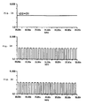
- Power supply unit 121 is constituted by a dc power supply such as a secondary battery, and as shown in FIG. 3A, continuously generates a typical 3.0 V power supply voltage.
- Clock generator 122 is supplied with the power supply voltage from power supply unit 121, and as shown in FIG. 3B, generates a reference clock signal of a predetermined duty cycle that alternates between the power-supply voltage and the ground voltage.
- Semiconductor booster circuit 100 receives as input both the power-supply voltage from power supply unit 121 and the reference clock signal from clock generator 122 and provides a doubled voltage in which the power-supply voltage has been substantially doubled. Data writing and data erasing are performed on FeRAM 131 at a voltage that is substantially twice that of the typical power-supply voltage. Write/erase circuit 132 performs data writing and data erasing in FeRAM 131 at the doubled voltage that is supplied from semiconductor booster circuit 100.
- the power-supply voltage is applied to power supply input terminal 101 from power supply unit 121, and the ground voltage is applied to ground potential terminal 102.
- the reference clock signal is applied as input from clock generator 122 to clock input terminal 103.
- Inverter 104 inverts the reference clock signal applied from clock input terminal 103, as shown in FIG. 3C.
- FET transistors 105 and 106 are constituted by non-doped n-channel FET transistors, and not only is the ground voltage constantly applied from ground potential terminal 102 to the back gates, but the power-supply voltage is constantly applied from power supply input terminal 101 to the source electrodes.
- the inverted clock signal is applied from inverter 104 to the gate electrode of FET transistor 105, the power-supply voltage applied from power supply input terminal 101 to the source electrode is conducted to the drain electrode when the inverted clock signal is at the power-supply voltage but is not conducted when the inverted clock signal is at the ground voltage.
- the power-supply voltage that is applied to the source electrode is not conducted to the drain electrode when the reference clock signal is at the ground voltage but is conducted when the reference clock at signal is at the power-supply voltage.
- Capacitor 107 has its one end connected to the drain electrode of FET transistor 105, and has its other end connected to clock input terminal 103. As a result, capacitor 107 stores the power-supply voltage supplied from power supply input terminal 101 by way of FET transistor 105 to one end of capacitor 107 when the reference clock signal becomes the ground voltage and the inverted clock signal becomes the power-supply voltage. On the other hand, capacitor 107 supplies the stored power-supply voltage together with the power-supply voltage of the reference clock signal to FET transistor 109 when the reference clock signal becomes the power-supply voltage.
- Capacitor 108 has its one end connected to the drain electrode of FET transistor 106 and has its other end connected to inverter 104. As a result, capacitor 108 stores the power-supply voltage supplied from power supply input terminal 101 by way of FET transistor 106 to one end of capacitor 108 when the reference clock signal becomes the power-supply voltage and the inverted clock signal becomes the ground voltage, and supplies the power-supply voltage to FET transistor 110 when the inverted clock signal becomes the power-supply voltage.
- capacitors 107 and 108 store the power-supply voltage supplied from power supply input terminal 101 and provide the power-supply voltage together with the power-supply voltage of the reference clock signal and the inverted clock signal, whereby the output voltage is substantially 6.0 V, or twice the power-supply voltage.
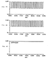
- a check of the operation of semiconductor booster circuit 100 by means of a computer simulation showed that the output voltage was approximately 5.9 V, as shown in the example of FIGs. 4 and 5.
- FET transistors 109 and 110 are constituted by p-channel transistors in which the source electrodes and back gates are connected each other.
- FET transistor 109 has its drain electrode connected to capacitor 107 and its gate electrode connected to capacitor 108.
- FET transistor 110 has its drain electrode connected to capacitor 108 and its gate electrode connected to capacitor 107.
- the drain voltage is conducted to the source electrode when the stored voltage of capacitor 107 applied to the drain electrode is higher than the voltage obtained by adding the threshold voltage to the gate voltage of this FET transistor, but the drain voltage is not conducted when the voltage is lower.
- the drain voltage of FET transistor 110 is conducted to the source electrode when the stored voltage of capacitor 108 applied to the drain electrode is higher than the voltage obtained by adding the threshold voltage to the stored voltage of capacitor 107 applied to the gate electrode, but is not conducted when the voltage is lower.
- FET transistors 109 and 110 therefore alternately conduct the output voltages of capacitors 107 and 108, whereby the output voltages of capacitors 107 and 108 alternate between the power-supply voltage and a doubled voltage in synchronous with the reference clock signal and inverted clock signal, as shown in FIGs. 4A and 4B as well as in FIGs. 5A and 5B.
- Capacitor 111 alternately stores the doubled voltage, which is the stored voltage of capacitor 107 and the doubled voltage, which is the stored voltage of capacitor 108, and external output terminal 112 continuously provides to the outside a doubled voltage, which is the stored voltage of capacitor 111, as shown in FIG. 5C.
- step-up power supply device 120 of the present embodiment power supply unit 121 generates the power-supply voltage, clock generator 122 generates the reference clock signal from the power-supply voltage, and the power-supply voltage and the reference clock signal are supplied to semiconductor booster circuit 100, whereby semiconductor booster circuit 100 provides to the outside a doubled voltage, which is the power-supply voltage boosted to substantially twice its original level.
- the power-supply voltage is constantly applied as input to power supply input terminal 101 as shown in FIG. 3A, and the reference clock signal applied as input to clock input terminal 103 is converted by inverter 104 to an inverted clock signal, as shown in FIGs. 3B and 3C.
- the power-supply voltage applied from power supply input terminal 101 to FET transistor 105 is stored in capacitor 107, and the stored voltage of capacitor 108 is delivered together with the power-supply voltage of the inverted clock signal from FET transistor 110 and through external output terminal 112.
- the power-supply voltage applied from power supply input terminal 101 to FET transistor 106 is stored in capacitor 108, and the stored voltage of capacitor 107 is delivered together with the power-supply voltage of reference clock signal from FET transistor 109 and through external output terminal 112.
- capacitors 107 and 108 thus alternately store the power-supply voltage of power supply input terminal 101 and alternately deliver the power-supply voltage together with the power-supply voltage of the reference clock signal and the inverted clock signal, a doubled voltage of substantially twice the power-supply voltage is continuously delivered from external output terminal 112, as shown in FIGS. 4A and 4B and FIGs. 5A and 5B.
- semiconductor booster circuit 100 of the present embodiment is capable of boosting the power-supply voltage to substantially twice its original level as described in the foregoing explanation, the circuit features simple construction and good productivity because it does not require FET transistor elements having a breakdown voltage of substantially twice the power-supply voltage.
- the connection of capacitor 111 to external output terminal 112, from which the doubled voltage is alternately delivered from capacitors 107 and 108, enables the output of a doubled voltage having excellent smoothness.
- write/erase circuit 132 executes data writing and data erasing of FeRAM 131 at the doubled voltage delivered to the outside by above-described step-up power supply device 120, thereby enabling data writing/erasing of FeRAM 131, which requires a voltage of approximately twice the typical power-supply voltage.
- semiconductor booster circuit 100 of the present embodiment was described using a case in which an inverted clock signal from inverter 104 was applied to the gate electrode of FET transistor 105 and the reference clock signal from clock input terminal 103 was applied to the gate electrode of FET transistor 106.
- the power-supply voltage may be applied from power supply input terminal 101 to both the gate electrodes and source electrodes of FET transistors 105 and 106.
- the stored voltage of capacitors 107 and 108 is applied to the drain electrodes of FET transistors 105 and 106, and as a result, the power-supply voltage of the source electrodes is conducted to the drain electrodes when the power-supply voltage applied to the gate electrodes and source electrodes is lower than the voltage obtained by subtracting the threshold voltage from the drain voltages.
- Semiconductor booster circuit 140 therefore functions in the same manner as the previously described semiconductor booster circuit 100, but enables a further simplification of construction and a further improvement in productivity to be achieved by merely connecting power supply input terminal 101 together with the source electrodes to the gate electrodes of FET transistors 105 and 106.
- FET transistors 105 and 106 may be replaced by diodes 151 and 152 having anodes connected to power supply input terminal 101 and cathodes connected to capacitor 107 and 108, as in semiconductor booster circuit 150 shown in FIG. 7.
- semiconductor booster circuit 150 functions in the same manner as the previously described semiconductor booster circuits 100 and 140, but a further simplification of circuit structure and a further improvement in productivity can be achieved.
Landscapes
- Engineering & Computer Science (AREA)
- Power Engineering (AREA)
- Dc-Dc Converters (AREA)
- Semiconductor Integrated Circuits (AREA)
- Read Only Memory (AREA)
Abstract
Description
Claims (11)
- A semiconductor booster circuit, comprising:a power supply input terminal for being supplied with a power-supply voltage ;a clock input terminal for being supplied with a reference clock signal of a predetermined duty cycle that alternates between said power-supply voltage and a ground voltage;a clock inverting circuit connected to said clock input terminal for providing a clock signal generated by inverting said reference clock signal;a first capacitor having its one end connected to said clock input terminal;a second capacitor having its one end connected to the output of said clock inverting circuit;a first FET transistor of a first conduction type having its drain electrode connected to the other end of said first capacitor and its gate electrode connected to the other end of said second capacitor;a second FET transistor of the first conduction type having its drain electrode connected to the other end of said second capacitor and its gate electrode connected to the other end of said first capacitor;a third FET transistor of a second conduction type having its source electrode connected to said power supply input terminal, its gate electrode connected to the output of said clock inverting circuit, and its drain electrode connected to the other end of said first capacitor, the drain electrode of said first FET transistor, and the gate electrode of said second FET transistor;a fourth FET transistor of the second conduction type having its source electrode connected to said power supply input terminal, its gate electrode connected to said clock input terminal, and its drain electrode connected to the other end of said second capacitor, the drain electrode of said second FET transistor, and the gate electrode of said first FET transistor; andan external output terminal connected to the source electrodes of said first and second FET transistors.
- A circuit according to claim 1, wherein said third and fourth FET transistors are turned on when said power-supply voltage is applied to said gate electrodes of said third and fourth FET transistors.
- A semiconductor booster circuit, comprising:a power supply input terminal for being supplied with a power-supply voltage ;a clock input terminal for being supplied with a reference clock signal of a predetermined duty cycle that alternates between said power-supply voltage and a ground voltage;a clock inverting circuit connected to said clock input terminal for providing a clock signal produced by inverting said reference clock signal;a first capacitor having its one end connected to said clock input terminal;a second capacitor having its one end connected to the output of said clock inverting circuit;a first FET transistor of a first conduction type having its drain electrode connected to the other end of said first capacitor and its gate electrode connected to the other end of said second capacitor;a second FET transistor of the first conduction type having its drain electrode connected to the other end of said second capacitor and its gate electrode connected to the other end of said first capacitor;a third FET transistor of a second conduction type having its gate and source electrodes connected to said power supply input terminal, and its drain electrode connected to the other end of said first capacitor, the drain electrode of said first FET transistor, and the gate electrode of said second FET transistor;a fourth FET transistor of the second conduction type having its gate and source electrodes connected to said power supply input terminal, and its drain electrode connected to the other end of said second capacitor, the drain electrode of said second FET transistor, and the gate electrode of said first FET transistor; andan external output terminal connected to the source electrodes of said first and second FET transistors.
- A circuit according to claim 3, wherein a threshold voltage of said third and fourth FET transistors is equal to or less than 0.5 V.
- A semiconductor booster circuit, comprising:a power supply input terminal for being supplied with a power-supply voltage ;a clock input terminal for being supplied with a reference clock signal of a predetermined duty cycle that alternates between said power-supply voltage and a ground voltage;a clock inverting circuit connected to said clock input terminal for providing a clock signal generated by inverting said reference clock signal;a first capacitor having its one end connected to said clock input terminal;a second capacitor having its one end connected to the output of said clock inverting circuit;a first FET transistor of a first conduction type having its drain electrode connected to the other end of said first capacitor and its gate electrode connected to the other end of said second capacitor;a second FET transistor of the first conduction type having its drain electrode connected to the other end of said second capacitor and its gate electrode connected to the other end of said first capacitor;a first diode having its anode connected to said power supply input terminal, and its cathode connected to the other end of said first capacitor, the drain electrode of said first FET transistor, and the gate electrode of said second FET transistor;a second diode having its anode connected to said power supply input terminal, and its cathode connected to the other end of said second capacitor, the drain electrode of said second FET transistor, and the gate electrode of said first FET transistor; andan external output terminal connected to the source electrodes of said first and said second FET transistors.
- A semiconductor booster circuit according to claim 1, further comprising a third capacitor connected between said external output terminal and a ground potential terminal.
- A semiconductor booster circuit according to claim 3, further comprising a third capacitor connected between said external output terminal and a ground potential terminal.
- A semiconductor booster circuit according to claim 5, further comprising a third capacitor connected between said external output terminal and a ground potential terminal.
- A step-up power supply device comprising:a semiconductor booster circuit according to claim 1;a power supply unit for generating a power-supply voltage and applying the power-supply voltage to the power supply input terminal of said semiconductor booster circuit; anda clock generation means for generating said reference clock signal from said power-supply voltage generated by said power supply unit and supplying said reference clock signal to the clock input terminal of said semiconductor booster circuit.
- A step-up power supply device comprising:a semiconductor booster circuit according to claim 3;a power supply unit for generating a power-supply voltage and applying the power-supply voltage to the power supply input terminal of said semiconductor booster circuit; anda clock generation means for generating said reference clock signal from said power-supply voltage generated by said power supply unit and supplying said reference clock signal to the clock input terminal of said semiconductor booster circuit.
- A step-up power supply device comprising:a semiconductor booster circuit according to claim 5;a power supply unit for generating a power-supply voltage and applying the power-supply voltage to the power supply input terminal of said semiconductor booster circuit; anda clock generation means for generating said reference clock signal from said power-supply voltage generated by said power supply unit and supplying said reference clock signal to the clock input terminal of said semiconductor booster circuit.
Applications Claiming Priority (2)
| Application Number | Priority Date | Filing Date | Title |
|---|---|---|---|
| JP2001364546A JP2003168288A (en) | 2001-11-29 | 2001-11-29 | Semiconductor boosting circuit, and boosting power source device |
| JP2001364546 | 2001-11-29 |
Publications (2)
| Publication Number | Publication Date |
|---|---|
| EP1318591A2 true EP1318591A2 (en) | 2003-06-11 |
| EP1318591A3 EP1318591A3 (en) | 2004-06-30 |
Family
ID=19174719
Family Applications (1)
| Application Number | Title | Priority Date | Filing Date |
|---|---|---|---|
| EP02026533A Withdrawn EP1318591A3 (en) | 2001-11-29 | 2002-11-27 | A semiconductor booster circuit requiring no transistor elements having a breakdown voltage of substantially twice the power supply voltage |
Country Status (4)
| Country | Link |
|---|---|
| US (1) | US6897708B2 (en) |
| EP (1) | EP1318591A3 (en) |
| JP (1) | JP2003168288A (en) |
| CN (1) | CN1421997A (en) |
Cited By (4)
| Publication number | Priority date | Publication date | Assignee | Title |
|---|---|---|---|---|
| WO2007145752A2 (en) | 2006-06-06 | 2007-12-21 | Skyworks Solutions, Inc. | Voltage up-conversion circuit using low voltage transistors |
| US9292079B2 (en) | 2013-09-13 | 2016-03-22 | Globalfoundries Inc. | Accelerating the microprocessor core wakeup by predictively executing a subset of the power-up sequence |
| US9389674B2 (en) | 2013-09-13 | 2016-07-12 | International Business Machines Corporation | Predictively turning off a charge pump supplying voltage for overdriving gates of the power switch header in a microprocessor with power gating |
| US9423865B2 (en) | 2013-09-13 | 2016-08-23 | Globalfoundries Inc. | Accelerating microprocessor core wake up via charge from capacitance tank without introducing noise on power grid of running microprocessor cores |
Families Citing this family (10)
| Publication number | Priority date | Publication date | Assignee | Title |
|---|---|---|---|---|
| US7719343B2 (en) | 2003-09-08 | 2010-05-18 | Peregrine Semiconductor Corporation | Low noise charge pump method and apparatus |
| KR101254652B1 (en) | 2006-07-05 | 2013-04-15 | 재단법인서울대학교산학협력재단 | Direct current converting circuit, display apparatus having the same and method of driving the direct current converting circuit |
| US9660590B2 (en) | 2008-07-18 | 2017-05-23 | Peregrine Semiconductor Corporation | Low-noise high efficiency bias generation circuits and method |
| US8816659B2 (en) | 2010-08-06 | 2014-08-26 | Peregrine Semiconductor Corporation | Low-noise high efficiency bias generation circuits and method |
| US20110199039A1 (en) * | 2010-02-17 | 2011-08-18 | Lansberry Geoffrey B | Fractional boost system |
| JP5197704B2 (en) * | 2010-09-22 | 2013-05-15 | 株式会社東芝 | Semiconductor device |
| US8686787B2 (en) * | 2011-05-11 | 2014-04-01 | Peregrine Semiconductor Corporation | High voltage ring pump with inverter stages and voltage boosting stages |
| JP6262992B2 (en) * | 2013-10-31 | 2018-01-17 | 浜松ホトニクス株式会社 | Booster circuit |
| US9917509B2 (en) * | 2016-05-26 | 2018-03-13 | Himax Technologies Limited | Charge pump circuit outputting high voltage without high voltage-endurance electric devices |
| CN107147282B (en) * | 2017-05-27 | 2019-07-19 | 普诚创智(成都)科技有限公司 | A kind of efficiently double capacitance charge pumps |
Family Cites Families (11)
| Publication number | Priority date | Publication date | Assignee | Title |
|---|---|---|---|---|
| US5267201A (en) * | 1990-04-06 | 1993-11-30 | Mosaid, Inc. | High voltage boosted word line supply charge pump regulator for DRAM |
| KR930008876B1 (en) * | 1990-08-17 | 1993-09-16 | 현대전자산업 주식회사 | High Voltage Generation Circuit of Semiconductor Device |
| IT1258242B (en) * | 1991-11-07 | 1996-02-22 | Samsung Electronics Co Ltd | SEMICONDUCTOR MEMORY DEVICE INCLUDING SUPPLY VOLTAGE PUMPING CIRCUIT |
| KR100285974B1 (en) * | 1992-11-18 | 2001-04-16 | 사와무라 시코 | Step-up Power Generation Circuit |
| US5436587A (en) * | 1993-11-24 | 1995-07-25 | Sundisk Corporation | Charge pump circuit with exponetral multiplication |
| US6208196B1 (en) | 1999-03-02 | 2001-03-27 | Maxim Integrated Products, Inc. | Current mode charge pumps |
| JP4242006B2 (en) * | 1999-06-23 | 2009-03-18 | 株式会社ルネサステクノロジ | Charge pump circuit and nonvolatile semiconductor memory device using the same |
| KR100340866B1 (en) * | 1999-12-02 | 2002-06-20 | 박종섭 | Boosted voltage generator |
| TW486869B (en) * | 1999-12-27 | 2002-05-11 | Sanyo Electric Co | Voltage producing circuit and a display device provided with such voltage producing circuit |
| KR100347144B1 (en) * | 2000-05-02 | 2002-08-03 | 주식회사 하이닉스반도체 | High voltage generating circuit |
| US6476666B1 (en) * | 2001-05-30 | 2002-11-05 | Alliance Semiconductor Corporation | Bootstrapped charge pump |
-
2001
- 2001-11-29 JP JP2001364546A patent/JP2003168288A/en active Pending
-
2002
- 2002-11-27 US US10/305,689 patent/US6897708B2/en not_active Expired - Fee Related
- 2002-11-27 EP EP02026533A patent/EP1318591A3/en not_active Withdrawn
- 2002-11-29 CN CN02152974.4A patent/CN1421997A/en active Pending
Cited By (8)
| Publication number | Priority date | Publication date | Assignee | Title |
|---|---|---|---|---|
| WO2007145752A2 (en) | 2006-06-06 | 2007-12-21 | Skyworks Solutions, Inc. | Voltage up-conversion circuit using low voltage transistors |
| EP2038719A4 (en) * | 2006-06-06 | 2012-10-10 | Skyworks Solutions Inc | Voltage up-conversion circuit using low voltage transistors |
| KR101375017B1 (en) * | 2006-06-06 | 2014-03-14 | 스카이워크스 솔루션즈, 인코포레이티드 | Voltage up-conversion circuit using low voltage transistors |
| US9292079B2 (en) | 2013-09-13 | 2016-03-22 | Globalfoundries Inc. | Accelerating the microprocessor core wakeup by predictively executing a subset of the power-up sequence |
| US9298253B2 (en) | 2013-09-13 | 2016-03-29 | Globalfoundries Inc. | Accelerating the microprocessor core wakeup by predictively executing a subset of the power-up sequence |
| US9389674B2 (en) | 2013-09-13 | 2016-07-12 | International Business Machines Corporation | Predictively turning off a charge pump supplying voltage for overdriving gates of the power switch header in a microprocessor with power gating |
| US9423865B2 (en) | 2013-09-13 | 2016-08-23 | Globalfoundries Inc. | Accelerating microprocessor core wake up via charge from capacitance tank without introducing noise on power grid of running microprocessor cores |
| US9471136B2 (en) | 2013-09-13 | 2016-10-18 | International Business Machines Corporation | Predictively turning off a charge pump supplying voltage for overdriving gates of the power switch header in a microprocessor with power gating |
Also Published As
| Publication number | Publication date |
|---|---|
| JP2003168288A (en) | 2003-06-13 |
| EP1318591A3 (en) | 2004-06-30 |
| US6897708B2 (en) | 2005-05-24 |
| CN1421997A (en) | 2003-06-04 |
| US20030098737A1 (en) | 2003-05-29 |
Similar Documents
| Publication | Publication Date | Title |
|---|---|---|
| US6897708B2 (en) | Semiconductor booster circuit requiring no transistor elements having a breakdown voltage of substantially twice the power supply voltage | |
| US6026002A (en) | Circuit configuration for supplying an electronic load circuit | |
| US6580654B2 (en) | Boosted voltage supply | |
| US5193198A (en) | Method and apparatus for reduced power integrated circuit operation | |
| KR930024010A (en) | Nonvolatile Semiconductor Memory | |
| JP3919323B2 (en) | Internal voltage supply circuit for semiconductor devices | |
| US20030123289A1 (en) | Nonvolatile semiconductor memory | |
| US7514984B2 (en) | Charge pumping circuit and direct current converting apparatus using the same | |
| JP2005235315A (en) | Boosting circuit | |
| US20050168265A1 (en) | Power supply circuit for oscillator of semiconductor memory device and voltage pumping device using the same | |
| JP2000078777A (en) | Voltage generator circuit | |
| JPS59167900A (en) | Method of generating high voltage state and dynamic load circuit | |
| KR970067346A (en) | Dynamic Random Access Memory | |
| KR100763331B1 (en) | Semiconductor memory device | |
| JP2723946B2 (en) | Circuit for charging the word line of EEPROM | |
| KR100610013B1 (en) | Charge pump circuit suitable for semiconductor memory | |
| KR100592772B1 (en) | High voltage generator | |
| US4823317A (en) | EEPROM programming switch | |
| JP3552789B2 (en) | High voltage generator | |
| US5638023A (en) | Charge pump circuit | |
| KR20010004448A (en) | An Invertor for outputting a high voltage | |
| TW494630B (en) | Semiconductor circuit including output buffer circuit and drive circuit for driving output buffer circuit | |
| JP2005129815A (en) | Charge pump circuit | |
| JP3764176B2 (en) | Semiconductor device | |
| JP4238869B2 (en) | Voltage generation circuit |
Legal Events
| Date | Code | Title | Description |
|---|---|---|---|
| PUAI | Public reference made under article 153(3) epc to a published international application that has entered the european phase |
Free format text: ORIGINAL CODE: 0009012 |
|
| AK | Designated contracting states |
Designated state(s): AT BE BG CH CY CZ DE DK EE ES FI FR GB GR IE IT LI LU MC NL PT SE SK TR |
|
| AX | Request for extension of the european patent |
Extension state: AL LT LV MK RO SI |
|
| PUAL | Search report despatched |
Free format text: ORIGINAL CODE: 0009013 |
|
| AK | Designated contracting states |
Kind code of ref document: A3 Designated state(s): AT BE BG CH CY CZ DE DK EE ES FI FR GB GR IE IT LI LU MC NL PT SE SK TR |
|
| AX | Request for extension of the european patent |
Extension state: AL LT LV MK RO SI |
|
| RIC1 | Information provided on ipc code assigned before grant |
Ipc: 7G 11C 5/14 B Ipc: 7H 02M 3/07 A |
|
| 17P | Request for examination filed |
Effective date: 20040518 |
|
| 17Q | First examination report despatched |
Effective date: 20041011 |
|
| AKX | Designation fees paid |
Designated state(s): DE FR GB |
|
| GRAP | Despatch of communication of intention to grant a patent |
Free format text: ORIGINAL CODE: EPIDOSNIGR1 |
|
| STAA | Information on the status of an ep patent application or granted ep patent |
Free format text: STATUS: THE APPLICATION IS DEEMED TO BE WITHDRAWN |
|
| 18D | Application deemed to be withdrawn |
Effective date: 20050909 |