EP1318440A1 - Architecture and method of managing an interface based on a finite states machine - Google Patents
Architecture and method of managing an interface based on a finite states machine Download PDFInfo
- Publication number
- EP1318440A1 EP1318440A1 EP01830744A EP01830744A EP1318440A1 EP 1318440 A1 EP1318440 A1 EP 1318440A1 EP 01830744 A EP01830744 A EP 01830744A EP 01830744 A EP01830744 A EP 01830744A EP 1318440 A1 EP1318440 A1 EP 1318440A1
- Authority
- EP
- European Patent Office
- Prior art keywords
- command
- clock
- circuits
- commands
- user
- Prior art date
- Legal status (The legal status is an assumption and is not a legal conclusion. Google has not performed a legal analysis and makes no representation as to the accuracy of the status listed.)
- Granted
Links
Images



Classifications
-
- G—PHYSICS
- G05—CONTROLLING; REGULATING
- G05B—CONTROL OR REGULATING SYSTEMS IN GENERAL; FUNCTIONAL ELEMENTS OF SUCH SYSTEMS; MONITORING OR TESTING ARRANGEMENTS FOR SUCH SYSTEMS OR ELEMENTS
- G05B19/00—Program-control systems
- G05B19/02—Program-control systems electric
- G05B19/04—Program control other than numerical control, i.e. in sequence controllers or logic controllers
- G05B19/045—Program control other than numerical control, i.e. in sequence controllers or logic controllers using logic state machines, consisting only of a memory or a programmable logic device containing the logic for the controlled machine and in which the state of its outputs is dependent on the state of its inputs or part of its own output states, e.g. binary decision controllers, finite state controllers
-
- G—PHYSICS
- G05—CONTROLLING; REGULATING
- G05B—CONTROL OR REGULATING SYSTEMS IN GENERAL; FUNCTIONAL ELEMENTS OF SUCH SYSTEMS; MONITORING OR TESTING ARRANGEMENTS FOR SUCH SYSTEMS OR ELEMENTS
- G05B2219/00—Program-control systems
- G05B2219/20—Pc systems
- G05B2219/23—Pc programming
- G05B2219/23245—Block, buffer the inputs when executing critical process, read them when finished, for a finite state machine
-
- G—PHYSICS
- G05—CONTROLLING; REGULATING
- G05B—CONTROL OR REGULATING SYSTEMS IN GENERAL; FUNCTIONAL ELEMENTS OF SUCH SYSTEMS; MONITORING OR TESTING ARRANGEMENTS FOR SUCH SYSTEMS OR ELEMENTS
- G05B2219/00—Program-control systems
- G05B2219/20—Pc systems
- G05B2219/23—Pc programming
- G05B2219/23289—State logic control, finite state, tasks, machine, fsm
-
- G—PHYSICS
- G11—INFORMATION STORAGE
- G11C—STATIC STORES
- G11C16/00—Erasable programmable read-only memories
- G11C16/02—Erasable programmable read-only memories electrically programmable
- G11C16/06—Auxiliary circuits, e.g. for writing into memory
Definitions
- the present invention relates to finite states machines and in particular to a method of managing and an interface based on a finite states machine.
- the interface performs a true handshake among the external circuits and one or more internal circuits.
- the interface assumes a basic role and any misfunctioning, even in just one of the tasks that it carries out, may in some cases cause an interruption of communications and consequently require a hardware reset of the whole integrated circuit a new start from the initial conditions.
- the state machine (briefly SM) is considered as a synchronous machine that receives its clock from the external world circuits and manages the interaction with the internal circuits in an asynchronous mode by resetting the bistable state circuits (FF) according to conditions based on information coming from the internal circuits.
- the SM reaches a state univocally determined by the setting of the FFprog, which causes the start of a certain embedded operation by the device.
- ENDOP signal End Operation
- the reset is done by means of a very short pulse (of minimum duration) as it will be better highlighted later.
- certain state FFs receive the user clock, other FFs have their own clock pin coupled to handshake signals with the internal circuits; such that upon an internal communication, a FF sets, instantaneously changing the global state of the machine but the same FF must be reset after propagation of the event through a circuit chain.
- Difficult testability if the whole interface could summarize its current state on a bus of state variables of a few bits concentrated in an homogeneous area, it would be easy, in test mode, to force a state, let the structure evolve and finally read the state in which the structure evolves after an evaluation.
- the above discussed approaches because of their inherent complexity clearly imply a difficult testability.
- a different approach followed by the present inventors that has been found outstandingly effective in overcoming the above discussed difficulties and drawbacks of the known approach is that of designing the interface circuit such to be, substantially definable as a SM working with a single CLK command and with a single reset command (the latter common to all the logic circuits of the device) solicitable to act, respecting the set up and hold times on the inputs, at a rate such that each new command does not arrive before the current evaluation has been correctly concluded.
- the method of managing a finite states machine commanded, according to the invention, through an "interface" or input arbitration circuit having a memory buffer in which any command to be carried out may be stored, by issuing a command through data inputs of the finite states machine and applying a clock signal to a single clock input of the finite states machine, comprises the following steps:
- the arbitration structure is like an efficient secretary capable of accepting the tasks and of communicating them to the employee only if necessary and if this person is not at the moment busy with other tasks. In this manner it is possible to reduce the stress and to improve the quality of the work of the employee. Comparably, the error probability of the device of the invention is drastically reduced by realizing an accurate SM (employee) and an efficient arbitration structure (secretary).
- the input arbitration structure manages the following situations that may be classified into groups:
- Figure 2 is a scheme of an interface architecture of the invention, characterized by the presence of an arbitration structure ARBITRO.
- the inputs and the outputs toward the finite states machine SM are provided with appropriate labels identifying the distinct input signals paths.
- Figure 3 depicts a possible circuit that realizes the structure ARBITRO of the interface of the invention of Figure 2.
- the different conditioned paths of commands may be recognized by looking at the respective zones contoured by a dotted and dashed perimeter in the general circuit diagram of Figure 3.
- GROUP 1 The zone of Figure 3 labeled GROUP 1 relates to the signal path stimulated by user commands arriving while the state machine is not carrying out any evaluation; by contrast when an evaluation is still in progress, such a path is disabled by the gate input with the signal Teval (see the block CLOCK GENERATOR).
- GROUP 3 The zone of Figure 3 labeled GROUP 3 relates to the signal path stimulated by commands coming from the internal circuitry while the SM is not carrying out any evaluation.
- the zone of Figure 3 labeled GROUP 2 relates to the signal path through which commands (user and other commands) arriving during evaluation of a previous command are stored.
- the signals Cond_i represent the conditions (determined by the internal state of the SM) that determine the temporary storage and the eventual successive delayed evaluation only if necessary.
- GROUP 4 relates to the signal path stimulated when suitable input signals must be provided to the SM because "internal" or delayed commands have been received.
- GROUP 5 relates to the circuit that generates the clock and the signal Teval to be sent to the SM.
- a start pulse is provided to the monostable A that generates the signal Sig_eval having a duration equal to Teval, that is long enough to carry out the evaluation (where evaluation means the propagation time through the registers of the SM plus the time needed by the input combinatory logic network to stabilize itself following a change of the state variables. In fact it must be considered that just after the time Teval has elapsed, a new evaluation may take place.
- the monostable signal shown in the lowest part of Figure 4 cannot be set for the whole Teval interval because all the paths that could set it are disabled during this time interval.
- the CLK_SM is nothing else than Sig_eval, thus the timing of the SM is similar to that illustrated in the diagrams of Figure 4.
- the two monostable pulses are generated in real time (as a matter of fact MON_B switches MON_A in order to avoid any glitches on the clock).
- the monostable pulse MON_A blocks any eventual interfering command towards the SM.
- the monostable pulse MON_B times the provision to the SM input datum in respect to the clock beat.
- the signal INTDATA which represents the information, is instantaneously set. After a time Tsu, determined by the monostable pulse MON_B, a clock pulse may be issued. In this case, the timing of the signal CLK_SM is determined by the difference (Teval - Tsu), therefore this difference must be greater than the evaluation time plus the stabilization time of the input combinatory logic network of the SM following variations of state variables.
- GROUP 3 command In the case of a GROUP 3 command, an user command or an internal command that cannot be neglected is received while an evaluation is still in progress.
- the information (command) is stored in memory elements (Flip-Flop) and only when the interval Teval of the operation in progress expires, the new evaluation may be started with the same execution characteristics of a GROUP 2 command.
- Figure 6 depicts the timing diagram relative to this third group.
- Figure 7 depicts a possible timing diagram of an external (user) command or request of evaluation or a GROUP 4 internal command.
- circuit depicted in Figure 3 is just a sample embodiment, in reality an arbitration structure ARBITRO with the above illustrated functions may be realized using circuits that may be adapted or optimized depending on specifications and preferences of the designer.
- the architecture of the invention has many advantages.
- An interface made according to this invention does not have windows of insensibility to commands as wide as a classic structure normally has because of the fact that a local reset pulse of finite duration masks eventual user commands.
- the reset signal of the SM is the same global reset signal of the whole logic circuit and does not switches during normal functioning.
- the window of indetermination of a structure realized according to the present invention is smaller than the crossing time of just a couple of fast logic gates (i.e. a fraction of nanosecond).
- arbitration structure ARBITRO may have in general a modular structure whereby it is always possible to make a new situation fit one of the four groups described above so that the circuit module for managing remains standardizable.
- Another advantage that may be underlined is the reduced silicon area requirement for realizing the SM.
- the possibility of describing the SM in a "standard” fashion allows for an optimized codification of all the states and thus it is possible to reduce the number of FF required.
- FLASH-EEPROM non volatile memory devices can manage, by means of their own internal logic circuitry, complex updating algorithms and generate autonomously the relatively high voltages that are needed for erasing and writing data.
- a first category may be represented by INTEL specifications and the other category by AMD specifications.
- a command PROGRAM relates to a programming operation of a word at a certain memory address. In this case the beginning of the operation is determined by the user. During the programming, before the microcontroller signals the end of the operation by the signal ENDOP, no user command may cause a change of state; nor software reset (reset sw) and suspension commands are admitted.
- ENDOP When ENDOP is received, there are two possibilities: if the algorithm was successfully concluded, the SM must return in IDLE condition, ready to start another operation; on the contrary, if the algorithm failed, the SM remains locked in modification state as long as the user, having detected the "fail", gives the F0 (reset sw) command to unlock it. Therefore, in one case is the microcontroller that unlocks it, in the other case is the user who does it.
- CHIPERASE that consists in canceling all memory sectors of the FLASH_EEPROM device; the managing, from the point of view of the command interpreter, is the same as for the command PROGRAM.
- BLOCKERASE Another allowed operation is BLOCKERASE that consists in canceling one or more memory sectors chosen by the user. It is surely more complex because of the various possibilities that are contemplated by the specification.
- the user After a pre-defined number of user commands, the user signals the address of a sector to be erased; if there is not any further intervention by the user, after a certain pre-established time (50 ⁇ s), the algorithm erases the selected sector. On the contrary, if the user indicates a different sector to be erased before 50 ⁇ s are elapsed, the counter restarts counting 50 ⁇ s, and so on for as many sectors the user wants to select. After 50 ⁇ s are elapsed from the last indication of a sector, the algorithm carries out the erasing. When the algorithm ends there are the two possibilities already described for the other operations of data modification. A substantial difference in respect to the other operations of modification consists in the fact that a suspension, ordered by the user, is acceptable while waiting for a TIMEOUT (thus the algorithm has not been started yet), as well as while the algorithm is in progress.
- ENDOP acts on the reset of the SM core and thus it is able to bring the SM to an IDLE state irrespectively of the evaluation that was in progress.
- AREA OCCUPATION The designer has a limited possibility of optimizing area occupation because he must consider all possible conditions using an approach that hardly leads to a standard SM definition. There are several memory elements with control pins conditioned in the most various manners and therefore they are difficult to be simplified even by an automatic optimization tool.
- DIFFICULT TESTABILITY The state in which the IC is at a given instant is determined by all the FF that have been used, which are numerous and not homogeneously disposed. Therefore, it is difficult to couple them to few output pins, as it happens in testmode. Moreover it is excessively laborious to make tests in which it is possible to force any initial condition and detect the future state in order to ascertain the correct functioning of the system.
- the interface architecture of the present invention eliminates or reduces in an extremely effective manner the above mentioned problems.
- the above discussed problems pertain to a digital structure with multiple clock and multiple reset, while, according to the approach of the present invention, the design of the CI structure is split in design of a distinct command arbitration structure (clock and data arbitration structure, in the case considered) and of a state machine functioning with a single clock and a single reset.
- the objective is thus to design an input arbitration structure that receives multiple clocks and multiple resets and communicates with a conventional SM using a single clock and a single reset.
- the input arbitration circuit (ARBITRO) performs the following functions:
- the arbitration circuit (ARBITRO) must behave in one of the three following ways:
- the only user command that may cause a change of state is that corresponding to the suspension code; any other user command must not change the state of the machine. It is then possible to decide in this case of not producing a useless evaluation.
- CWE_N is the user clock that, when a command is produced, switches high.
- PULSE_GEN transforms a rising transition in a pulse having a short duration that varies with temperature and the supply voltage. The duration of such a pulse does not have to be particularly precise. If the signal MASK_N is high, that is the command is not masked, the result is a simple pulse on the signal USRTRANS.
- the portion of the circuit bordered by a dashed line that produces the signal MASK_N may even be omitted depending on what is contemplated in the design of the SM. Preferably this portion of the circuit is present because it is safer to filter the request than making an evaluation that leaves the state of the SM unchanged (as any other command while a programming is in progress).
- the mask does not leave user commands pass in all modification states while an algorithm is in progress except in case of a suspension during the BLOCKERASE operation. If the algorithm has terminated and a FAIL has been generated, user commands must pass because a F0 is necessary to unlock the SM.
- CUIFAIL is the output signal of the SM that is set only when the algorithm ends in an unsuccessfully manner.
- the signal SUSPEND_X is generated by a decoder that recognizes the code of the suspension command on the data bus. Given that the user must provide codes with an advance time Tsu before the clock pulse, the mask is surely in steady conditions when the front edge of CWE_N is received.
- TIMEOUT_TRANS If any evaluation is in progress, there is a pulse on TIMEOUT_TRANS. If an evaluation has been started or if an evaluation is still in progress, such a pulse does not pass on TIMEOUT_TRANS. This is allowed by the specifications, because having an evaluation in progress when TIMEOUT is received means that the user has given a command (in fact the microcontroller cannot be the cause of the evaluation because in this phase any modification has not been started yet).
- a command may be a suspension, and in this case the TIMEOUT must not be waited anylonger; or a new sector to be canceled, and in this case the counting must be reset and thus it is correct to lose the TIMEOUT that could be received in this phase; or any other command must return the SM in IDLE state, therefore even in this case the TIMEOUT is ignored.
- Teval quickly switches S1 low.
- FALSE-TIMEOUT-TRANS may be present a stretcher circuit that stretches the pulse, in the sense that it leaves unchanged the leading edge and delays the trailing edge; this better ensures the propagation of information.
- circuit structures described so far represent the possible paths leading to the generation of pulses on one of the four intermediate signal paths that, in some way, must determine the generation of output signals from the arbitration structure ARBITRO.
- the remaining portions of the arbitration structure respectively establish the clock and the supplementary input signals, to be provided to the SM to enable it carry out the required evaluation.
- the function that determines the clock CLOCK_TO_SM that is sent to the timing input of the SM is the logic difference between the outputs of two monostables: the monostable MON_A, that has a time duration Toper that represents the time needed to carry out completely an operation; the monostable MON_B, that has a time duration defined by the fact that when it is necessary to provide inputs to the SM, they must be provided in advance of a set up time.
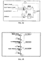
- Tsu the maximum set up time required by the fake inputs that are those established by the circuit of zone 5 of Figure 9 and shown in Figure 15, that is:
- the MON_B remains idle and the CLK_TO_SM will coincide with the pulse of MON_A. Because the output CLOCK has a minimum delay in respect to the user clock (CWE_N), the set up and hold times of the data provided by the user are practically unchanged in respect to the user clock.
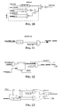
- FIG 16 illustrates the timing in case of real time user commands (GROUP A1).
- the pulse shall determine the almost simultaneous switching of the two monostables and the CLK_TO_SM will be that depicted in the time diagram of Figure 17, delayed by T_MON_B, that is by Tsu in respect to the leading edge of MON_A.
- Tsu is the time between the fake datum and the leading edge of the clock.
- the small delay of Figures 9 and 14 ensures that MON_B starts just ahead of MON_A, in order to prevent the generation of glitches on the clock.
- Such resets are obtained by signals determined by the SM that are set only when the evaluation that has been stored is started.
- the signal RES_FLAG_ENDOP_N resets FLAG_ENDOP only when RES_CUIFLAG is set that is a signal active in the IDLE or ERASESUSPEND state, or when CUIFAIL is set. When this last signal switches high, it means that a fail has occurred but also that a command coming from the microcontroller has been evaluated.
- the signal RES_SUSP_FLAG_N is determined by a signal SUSP_REQ that the SM sets at the moment of the occurred suspension.
- the FF may be reset if the system goes to the IDLE state (whereby the SM sets RES_CUIFLAG) or if a
- the ENDOP is processed and, no fail having been generated, the system returns to the IDLE state.
- the main advantage of the illustrated solution is that of allowing the realization of a SM with a single clock and a single reset from which all the positive effects derive.
- the conventional character of the structure implies an improved controllability of all the situations and thus lesser of design errors and bugs. It allows to use a standard SM structure depending on needs instead of a hybrid structure; moreover, it brings about a reduction of the occupied area because any design synthesizer tool will be able to optimize a conventional SM.
- a further advantage is the nullification, or at least a strong reduction, of situations in which indispensable commands may be lost and in which it is possible to be halted in a state from which it is possible to exit only with a hardware reset.
- test modes As far as the test modes are concerned, if the complexity of the specifications implies a 2 ⁇ N number of states, in order to know exactly the instantaneous working condition of the command interpreter, it is sufficient to output N signals that are those on which are encoded all possible states. It is also possible to force, in testmode, the state variables through N inputs and successively to provide a clock pulse to switch to the future state. It is possible to verify the correctness of the evaluation by inputting through the dedicated pads the new state variable. In other words, the designer has the possibility of implementing, with a low cost, a good controllability and inspectability of the command interpreter.
- Any flip-flop except those of the SM and of the arbitration structure, will be present in the hierarchy of the command interpreter and will undergo controls or conditionings depending on particular situations.
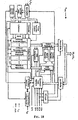
- Figure 18 depicts a high level functional block diagram of a FLASH_EEPROM non volatile memory device of the family of commercial devices 28F400B3, 28F800B3, called "SMART 3 ADVANCED BOOT BLOCK", produced by INTEL CORP.
- SMART 3 ADVANCED BOOT BLOCK produced by INTEL CORP.
- FIG. 18 depicts a high level functional block diagram of a FLASH_EEPROM non volatile memory device of the family of commercial devices 28F400B3, 28F800B3, called "SMART 3 ADVANCED BOOT BLOCK", produced by INTEL CORP.
- COMMAND USER INTERFACE functional block called COMMAND USER INTERFACE that is typically present in such non volatile memory devices, even of others manufacturers.
- the block COMMAND USER INTERFACE of a non volatile memory device of FLASH_EEPROM type has advantageously an architecture as that described herein and illustrated in Figures 9-17.
Landscapes
- Physics & Mathematics (AREA)
- General Physics & Mathematics (AREA)
- Engineering & Computer Science (AREA)
- Automation & Control Theory (AREA)
- Information Transfer Systems (AREA)
- Bus Control (AREA)
Abstract
Description
- detecting all the requests coming from external worlds;
- detecting the condition (free or in the course of carrying out an evaluation) of
the single clock SM and, depending on it, sorting and cueing the requests,
while respecting two main aims:
- passing commands to the SM only when it is able to carry them out (that is when there is not any other evaluation in progress) and eventually providing the data (on respective inputs of the SM) necessary to produce a correct evaluation;
- detecting all the requests and deciding which to store for carrying it out as soon as possible and which to filter (eliminate) if recognized as influent or useless.
- masking eventual further commands to the SM for a time Teval sufficient to carry out the evaluation;
- transmitting the clock edge in the form of a monostable signal to the SM.
- masking eventual further commands to the SM for a time Teval sufficient to carry out the evaluation;
- providing the information in input to the SM in a real time fashion;
- issuing a clock pulse to the SM after a certain time interval Tsu.
- storing the request in a real time fashion;
- waiting for the end of the operation in progress;
- providing the stored information (that can be defined as INTDATA) to the SM;
- issuing a clock pulse to the SM after a certain time interval Tsu;
- resetting the buffer storing the already used information.
- ignoring the request and doing nothing.
- a microcontroller that, depending on the task to be performed, carries out an appropriate sequence of operations or steps (algorithm);
- a counter for managing, among other things, the timing of application of high voltages to specific circuit nodes. In certain FLASH memories there are specific logic circuitries for managing the protection and other functions. Among said digital structures there is also an interface structure, commonly known as "command interpreter" (CI) that, depending on more or less complex specifications, recognizes (by way of codes) the operations that the user requires, and establishes a handshake with pertinent digital circuits. For example, according to certain specifications, once the sequence of commands corresponding to an erasing operation has been detected, the CI starts a counter, waits for a signal TIMEOUT and communicates to the microcontroller a state of readiness to run the relative code. The communication ends with the end of the operation, signaled by the microcontroller to the command interpreter.
- in memory devices of the first kind (INTEL), when an operation ends, for example a program operation, the CI must not "react" by changing its state immediately but it will do so only after an user command is received that makes the SM return to its initial state;
- in memory devices of the second kind (AMD), in the same situation, the CI must change its state by returning to a IDLE state without any user command; indeed, when the operation ends, may start immediately a new sequence of commands that must be accepted.
- providing a single clock (CLK);
- providing supplementary input data to the SM with appropriate set up and hold;
- separating the evaluation operations in order to carry them out one at the time.
- user commands while SM is not evaluating;
- end count command from the counter (TIMEOUT) while SM is not evaluating;
- command from the microcontroller (e.g. ENDOP) while SM is not evaluating;
- command from the microcontroller while SM is evaluating;
- user suspension command (SUSPEND) while a previous counter command is being executed;
- any user command, except a SUSPEND, while an evaluation is in progress;
- command from the counter while an evaluation is in progress.
- masking other possible commands for a time Teval;
- providing a clock pulse to the SM in a real time mode;
- masking other possible commands for a time Teval;
- providing the input datum to the SM in a real time mode;
- providing a clock pulse to the SM after a time Tsu.
- storing the request in real time mode;
- waiting for the end of the operation in progress;
- providing the input datum to the SM in real time mode;
- providing a clock pulse to the SM after a time Tsu.
- ignoring the command and doing nothing.
- OLD_SUSPEND (for an evaluation of deferred suspension);
- ENDOPDATA (for an evaluation due to a command of the microcontroller);
- CUI_TIMEOUT (for an evaluation determined by the counter).
Claims (4)
- An interface comprising a finite states machine and logic circuits for adapting it to a given specification, for managing asynchronous and independent interactions between external circuits, by way of user commands, and a plurality of internal circuits each functioning with a clock generally different from the clock of other internal circuits, of an integrated digital system, characterized in that said finite states machine is defined to work with a unique clock and unique reset and by the fact that said interface further comprises
an arbitration structure of the input signal provided to the finite states machine, comprising a memory buffer in which any user command or any command or datum, generated by any one of said internal circuits issued during a phase in which said finite states machine is carrying out an evaluation is stored. - The interface according to claim 1, wherein said arbitration structure realizes a plurality of distinct paths for said user commands coming from external circuits and for said commands and data coming from said internal circuits through chains of combinatory logic circuits and/or clocked logic circuits and/or memory bistable circuits, adapted to make the use of an evaluating finite state machine with single clock and single reset compatible with the different types and different timing of said commands and data, according to said specification.
- A FLASH_EEPROM device comprising a command interpreter circuit for recognizing, according to a given specification, the operations required from the memory device through command codes and implementing a handshake with corresponding digital circuits that constitute the memory device, each functioning with its own clock, generally different from the one another, characterized in that said command interpreter circuit comprises a single clock and a single reset finite state machine and an arbitration structure of the clock signals of said digital circuits from which commands come from, providing to said finite state machine said single clock and said single reset signals.
- A method of managing a finite state machine through an input arbitration structure having a memory buffer for storing a command to be executed by feeding codes and/or data to respective inputs of said finite state machine and a clock signal to a timing input of said finite state machine, comprising the following steps:a) for each new command verifying whether it is received while the state machine is carrying out a previous command or not;b) if the test of point a) is negative, issuing the command to the finite states machine in real time mode in the form of a clock pulse or in the form of an input datum and a clock pulse depending on whether it is an user command or a command coming from internal circuitry, respectively, and restarting a new cycle from point a);c) if the test of point a) is positive, verifying whether the new command can be ignored or not;d) if the test of point c) is negative, storing the command in said buffer, waiting for the state machine to end the execution of the previous command, issuing the deferred command to the state machine in the form of an input datum and of a clock pulse, erasing said command from the buffer and restarting a new cycle from point a).
Priority Applications (3)
| Application Number | Priority Date | Filing Date | Title |
|---|---|---|---|
| EP01830744A EP1318440B1 (en) | 2001-12-04 | 2001-12-04 | Architecture and method of managing an interface based on a finite states machine |
| DE60112771T DE60112771D1 (en) | 2001-12-04 | 2001-12-04 | Architecture and method for managing an interface based on a finite state machine |
| US10/309,759 US7284144B2 (en) | 2001-12-04 | 2002-12-04 | Finite state machine interface has arbitration structure to store command generated by internal circuits during evaluation phase of state machine for FLASH EEPROM device |
Applications Claiming Priority (1)
| Application Number | Priority Date | Filing Date | Title |
|---|---|---|---|
| EP01830744A EP1318440B1 (en) | 2001-12-04 | 2001-12-04 | Architecture and method of managing an interface based on a finite states machine |
Publications (2)
| Publication Number | Publication Date |
|---|---|
| EP1318440A1 true EP1318440A1 (en) | 2003-06-11 |
| EP1318440B1 EP1318440B1 (en) | 2005-08-17 |
Family
ID=8184797
Family Applications (1)
| Application Number | Title | Priority Date | Filing Date |
|---|---|---|---|
| EP01830744A Expired - Lifetime EP1318440B1 (en) | 2001-12-04 | 2001-12-04 | Architecture and method of managing an interface based on a finite states machine |
Country Status (3)
| Country | Link |
|---|---|
| US (1) | US7284144B2 (en) |
| EP (1) | EP1318440B1 (en) |
| DE (1) | DE60112771D1 (en) |
Cited By (1)
| Publication number | Priority date | Publication date | Assignee | Title |
|---|---|---|---|---|
| EP1868051A1 (en) * | 2006-06-15 | 2007-12-19 | Société Nationale des Chemins de Fer Français | Method for validating a control system and control system to be validated by this method |
Families Citing this family (5)
| Publication number | Priority date | Publication date | Assignee | Title |
|---|---|---|---|---|
| US7801835B2 (en) * | 2005-06-15 | 2010-09-21 | International Business Machines Corporation | Method for constructing autonomic advisors and learning procedural knowledge from scored examples |
| US7414891B2 (en) | 2007-01-04 | 2008-08-19 | Atmel Corporation | Erase verify method for NAND-type flash memories |
| US8005995B2 (en) | 2007-08-16 | 2011-08-23 | Micron Technology, Inc. | Command interface systems and methods |
| US7590789B2 (en) * | 2007-12-07 | 2009-09-15 | Intel Corporation | Optimizing clock crossing and data path latency |
| US9122797B2 (en) * | 2008-09-30 | 2015-09-01 | Honeywell International Inc. | Deterministic remote interface unit emulator |
Citations (1)
| Publication number | Priority date | Publication date | Assignee | Title |
|---|---|---|---|---|
| US5333300A (en) * | 1991-02-11 | 1994-07-26 | Intel Corporation | Timing circuitry and method for controlling automated programming and erasing of a non-volatile semiconductor memory |
Family Cites Families (9)
| Publication number | Priority date | Publication date | Assignee | Title |
|---|---|---|---|---|
| US4818932A (en) * | 1986-09-25 | 1989-04-04 | Tektronix, Inc. | Concurrent memory access system |
| US5237670A (en) * | 1989-01-30 | 1993-08-17 | Alantec, Inc. | Method and apparatus for data transfer between source and destination modules |
| US5386518A (en) * | 1993-02-12 | 1995-01-31 | Hughes Aircraft Company | Reconfigurable computer interface and method |
| US5796992A (en) * | 1995-12-20 | 1998-08-18 | Compaq Computer Corporation | Circuit for switching between synchronous and asynchronous memory refresh cycles in low power mode |
| US6243829B1 (en) * | 1998-05-27 | 2001-06-05 | Hewlett-Packard Company | Memory controller supporting redundant synchronous memories |
| US6779125B1 (en) * | 2000-06-09 | 2004-08-17 | Cirrus Logic, Inc. | Clock generator circuitry |
| US7007131B2 (en) * | 2000-12-27 | 2006-02-28 | Intel Corporation | Method and apparatus including special programming mode circuitry which disables internal program verification operations by a memory |
| US7007111B2 (en) * | 2001-06-11 | 2006-02-28 | Lsi Logic Corporation | DMA port sharing bandwidth balancing logic |
| JP3732139B2 (en) * | 2001-10-29 | 2006-01-05 | 三菱電機株式会社 | Memory control circuit and memory bus arbitration method |
-
2001
- 2001-12-04 EP EP01830744A patent/EP1318440B1/en not_active Expired - Lifetime
- 2001-12-04 DE DE60112771T patent/DE60112771D1/en not_active Expired - Lifetime
-
2002
- 2002-12-04 US US10/309,759 patent/US7284144B2/en not_active Expired - Lifetime
Patent Citations (1)
| Publication number | Priority date | Publication date | Assignee | Title |
|---|---|---|---|---|
| US5333300A (en) * | 1991-02-11 | 1994-07-26 | Intel Corporation | Timing circuitry and method for controlling automated programming and erasing of a non-volatile semiconductor memory |
Non-Patent Citations (2)
| Title |
|---|
| NOWICK S M ET AL: "Synthesis of asynchronous state machines using a local clock", PROCEEDINGS OF THE INTERNATIONAL CONFERENCE ON COMPUTER DESIGN - VLSI IN COMPUTERS AND PROCESSORS. CAMBRIDGE, MA., OCT. 14 - 16, 1991, LOS ALAMITOS, IEEE. COMP. SOC. PRESS, US, 14 October 1991 (1991-10-14), pages 192 - 197, XP010025205, ISBN: 0-8186-2270-9 * |
| TINDER R F ET AL: "HIGH-SPEED MICROPROGRAMMABLE ASYNCHRONOUS CONTROLLER MODULES", IEEE TRANSACTIONS ON COMPUTERS, IEEE INC. NEW YORK, US, vol. 43, no. 10, 1 October 1994 (1994-10-01), pages 1226 - 1232, XP000474493, ISSN: 0018-9340 * |
Cited By (2)
| Publication number | Priority date | Publication date | Assignee | Title |
|---|---|---|---|---|
| EP1868051A1 (en) * | 2006-06-15 | 2007-12-19 | Société Nationale des Chemins de Fer Français | Method for validating a control system and control system to be validated by this method |
| WO2007144513A3 (en) * | 2006-06-15 | 2008-02-07 | Sncf | Method of validating a control/command system and control/command system that can be validated by the method |
Also Published As
| Publication number | Publication date |
|---|---|
| US20030126204A1 (en) | 2003-07-03 |
| DE60112771D1 (en) | 2005-09-22 |
| EP1318440B1 (en) | 2005-08-17 |
| US7284144B2 (en) | 2007-10-16 |
Similar Documents
| Publication | Publication Date | Title |
|---|---|---|
| CN114286992B (en) | Daisy-chaining complex commands | |
| US4691124A (en) | Self-compensating, maximum speed integrated circuit | |
| US4748417A (en) | Method and circuit arrangement for switching a clock-controlled device having a plurality of operating statuses | |
| JPH0481932A (en) | Interruption controller | |
| EP1318440B1 (en) | Architecture and method of managing an interface based on a finite states machine | |
| JPH08125674A (en) | Communication controller | |
| CN101206614B (en) | Simulator for simulating register with specific function | |
| JPH07104830B2 (en) | Computer system and method of operating a computer system | |
| US20050099833A1 (en) | Memory device accessible with different communication protocols | |
| CN111049718B (en) | CAN bus simulation monitoring method | |
| CN111736655B (en) | Configuration method applied to clock chip | |
| CN116955032A (en) | Chip with debugging function and chip debugging method | |
| JP5917325B2 (en) | Bridge circuit | |
| US7945718B2 (en) | Microcontroller waveform generation | |
| US7770147B1 (en) | Automatic generators for verilog programming | |
| US8635597B2 (en) | Method for determining the processing order of modules in a function plan and electronic data processing system for carrying out the method | |
| EP0554819A1 (en) | Transfer control unit, processor element and data transferring method | |
| US11467620B1 (en) | Architecture and methodology for tuning clock phases to minimize latency in a serial interface | |
| CN111158339A (en) | CAN bus simulation monitoring system | |
| CN119670685A (en) | A verification method and system | |
| CN110471865B (en) | Method for realizing communication between controller and driver by simulating SPI communication | |
| CN121597285A (en) | Write command synchronous updating method and system applied to CSR register array | |
| SU1310835A1 (en) | Computer-computer interface | |
| Ecker | Semi-dynamic scheduling of synchronization-mechanisms | |
| KR100218383B1 (en) | PL C's Multi CUI Module System |
Legal Events
| Date | Code | Title | Description |
|---|---|---|---|
| PUAI | Public reference made under article 153(3) epc to a published international application that has entered the european phase |
Free format text: ORIGINAL CODE: 0009012 |
|
| AK | Designated contracting states |
Designated state(s): AT BE CH CY DE DK ES FI FR GB GR IE IT LI LU MC NL PT SE TR |
|
| AX | Request for extension of the european patent |
Extension state: AL LT LV MK RO SI |
|
| 17P | Request for examination filed |
Effective date: 20031201 |
|
| AKX | Designation fees paid |
Designated state(s): DE FR GB IT |
|
| 17Q | First examination report despatched |
Effective date: 20040203 |
|
| GRAP | Despatch of communication of intention to grant a patent |
Free format text: ORIGINAL CODE: EPIDOSNIGR1 |
|
| GRAS | Grant fee paid |
Free format text: ORIGINAL CODE: EPIDOSNIGR3 |
|
| GRAA | (expected) grant |
Free format text: ORIGINAL CODE: 0009210 |
|
| AK | Designated contracting states |
Kind code of ref document: B1 Designated state(s): DE FR GB IT |
|
| REG | Reference to a national code |
Ref country code: GB Ref legal event code: FG4D |
|
| REF | Corresponds to: |
Ref document number: 60112771 Country of ref document: DE Date of ref document: 20050922 Kind code of ref document: P |
|
| PG25 | Lapsed in a contracting state [announced via postgrant information from national office to epo] |
Ref country code: DE Free format text: LAPSE BECAUSE OF FAILURE TO SUBMIT A TRANSLATION OF THE DESCRIPTION OR TO PAY THE FEE WITHIN THE PRESCRIBED TIME-LIMIT Effective date: 20051118 |
|
| ET | Fr: translation filed | ||
| PLBE | No opposition filed within time limit |
Free format text: ORIGINAL CODE: 0009261 |
|
| STAA | Information on the status of an ep patent application or granted ep patent |
Free format text: STATUS: NO OPPOSITION FILED WITHIN TIME LIMIT |
|
| 26N | No opposition filed |
Effective date: 20060518 |
|
| PGFP | Annual fee paid to national office [announced via postgrant information from national office to epo] |
Ref country code: IT Payment date: 20071211 Year of fee payment: 7 |
|
| PGFP | Annual fee paid to national office [announced via postgrant information from national office to epo] |
Ref country code: GB Payment date: 20081125 Year of fee payment: 8 |
|
| PGFP | Annual fee paid to national office [announced via postgrant information from national office to epo] |
Ref country code: FR Payment date: 20081224 Year of fee payment: 8 |
|
| GBPC | Gb: european patent ceased through non-payment of renewal fee |
Effective date: 20091204 |
|
| REG | Reference to a national code |
Ref country code: FR Ref legal event code: ST Effective date: 20100831 |
|
| PG25 | Lapsed in a contracting state [announced via postgrant information from national office to epo] |
Ref country code: FR Free format text: LAPSE BECAUSE OF NON-PAYMENT OF DUE FEES Effective date: 20091231 |
|
| PG25 | Lapsed in a contracting state [announced via postgrant information from national office to epo] |
Ref country code: GB Free format text: LAPSE BECAUSE OF NON-PAYMENT OF DUE FEES Effective date: 20091204 |
|
| PG25 | Lapsed in a contracting state [announced via postgrant information from national office to epo] |
Ref country code: IT Free format text: LAPSE BECAUSE OF NON-PAYMENT OF DUE FEES Effective date: 20081204 |