EP1317002A2 - Poly-silicon layer of a thin film transistor and display device having the same - Google Patents
Poly-silicon layer of a thin film transistor and display device having the same Download PDFInfo
- Publication number
- EP1317002A2 EP1317002A2 EP02090384A EP02090384A EP1317002A2 EP 1317002 A2 EP1317002 A2 EP 1317002A2 EP 02090384 A EP02090384 A EP 02090384A EP 02090384 A EP02090384 A EP 02090384A EP 1317002 A2 EP1317002 A2 EP 1317002A2
- Authority
- EP
- European Patent Office
- Prior art keywords
- poly
- silicon layer
- channel region
- active channel
- layer according
- Prior art date
- Legal status (The legal status is an assumption and is not a legal conclusion. Google has not performed a legal analysis and makes no representation as to the accuracy of the status listed.)
- Granted
Links
Images


Classifications
-
- H—ELECTRICITY
- H10—SEMICONDUCTOR DEVICES; ELECTRIC SOLID-STATE DEVICES NOT OTHERWISE PROVIDED FOR
- H10D—INORGANIC ELECTRIC SEMICONDUCTOR DEVICES
- H10D30/00—Field-effect transistors [FET]
- H10D30/60—Insulated-gate field-effect transistors [IGFET]
- H10D30/67—Thin-film transistors [TFT]
-
- H—ELECTRICITY
- H10—SEMICONDUCTOR DEVICES; ELECTRIC SOLID-STATE DEVICES NOT OTHERWISE PROVIDED FOR
- H10D—INORGANIC ELECTRIC SEMICONDUCTOR DEVICES
- H10D30/00—Field-effect transistors [FET]
- H10D30/60—Insulated-gate field-effect transistors [IGFET]
- H10D30/67—Thin-film transistors [TFT]
- H10D30/6729—Thin-film transistors [TFT] characterised by the electrodes
- H10D30/673—Thin-film transistors [TFT] characterised by the electrodes characterised by the shapes, relative sizes or dispositions of the gate electrodes
- H10D30/6731—Top-gate only TFTs
-
- H—ELECTRICITY
- H10—SEMICONDUCTOR DEVICES; ELECTRIC SOLID-STATE DEVICES NOT OTHERWISE PROVIDED FOR
- H10D—INORGANIC ELECTRIC SEMICONDUCTOR DEVICES
- H10D30/00—Field-effect transistors [FET]
- H10D30/60—Insulated-gate field-effect transistors [IGFET]
- H10D30/67—Thin-film transistors [TFT]
- H10D30/674—Thin-film transistors [TFT] characterised by the active materials
- H10D30/6741—Group IV materials, e.g. germanium or silicon carbide
- H10D30/6743—Silicon
- H10D30/6745—Polycrystalline or microcrystalline silicon
-
- H—ELECTRICITY
- H10—SEMICONDUCTOR DEVICES; ELECTRIC SOLID-STATE DEVICES NOT OTHERWISE PROVIDED FOR
- H10D—INORGANIC ELECTRIC SEMICONDUCTOR DEVICES
- H10D30/00—Field-effect transistors [FET]
- H10D30/60—Insulated-gate field-effect transistors [IGFET]
- H10D30/67—Thin-film transistors [TFT]
- H10D30/6757—Thin-film transistors [TFT] characterised by the structure of the channel, e.g. transverse or longitudinal shape or doping profile
-
- H—ELECTRICITY
- H10—SEMICONDUCTOR DEVICES; ELECTRIC SOLID-STATE DEVICES NOT OTHERWISE PROVIDED FOR
- H10D—INORGANIC ELECTRIC SEMICONDUCTOR DEVICES
- H10D62/00—Semiconductor bodies, or regions thereof, of devices having potential barriers
- H10D62/40—Crystalline structures
-
- H—ELECTRICITY
- H10—SEMICONDUCTOR DEVICES; ELECTRIC SOLID-STATE DEVICES NOT OTHERWISE PROVIDED FOR
- H10D—INORGANIC ELECTRIC SEMICONDUCTOR DEVICES
- H10D86/00—Integrated devices formed in or on insulating or conducting substrates, e.g. formed in silicon-on-insulator [SOI] substrates or on stainless steel or glass substrates
- H10D86/01—Manufacture or treatment
- H10D86/021—Manufacture or treatment of multiple TFTs
- H10D86/0221—Manufacture or treatment of multiple TFTs comprising manufacture, treatment or patterning of TFT semiconductor bodies
- H10D86/0223—Manufacture or treatment of multiple TFTs comprising manufacture, treatment or patterning of TFT semiconductor bodies comprising crystallisation of amorphous, microcrystalline or polycrystalline semiconductor materials
- H10D86/0229—Manufacture or treatment of multiple TFTs comprising manufacture, treatment or patterning of TFT semiconductor bodies comprising crystallisation of amorphous, microcrystalline or polycrystalline semiconductor materials characterised by control of the annealing or irradiation parameters
-
- H—ELECTRICITY
- H10—SEMICONDUCTOR DEVICES; ELECTRIC SOLID-STATE DEVICES NOT OTHERWISE PROVIDED FOR
- H10D—INORGANIC ELECTRIC SEMICONDUCTOR DEVICES
- H10D86/00—Integrated devices formed in or on insulating or conducting substrates, e.g. formed in silicon-on-insulator [SOI] substrates or on stainless steel or glass substrates
- H10D86/01—Manufacture or treatment
- H10D86/021—Manufacture or treatment of multiple TFTs
- H10D86/0251—Manufacture or treatment of multiple TFTs characterised by increasing the uniformity of device parameters
Definitions
- the present invention relates to a poly-silicon layer and a device having the same, and more particularly, to a poly-silicon layer of a thin film transistor (TFT) and a device having the same.
- TFT thin film transistor
- An active channel region of a thin film transistor is generally made of a poly-silicon material and so includes grain boundaries. In the grain boundaries, defects such as dangling bonds and strained bonds exist, and such defects act as traps of the charge carriers.
- parameters such as grain size, grain-size uniformity, number of grains, locations of grain boundaries, and tilt angle of grain boundaries affect characteristics of the TFT such as threshold voltage, sub-threshold slope, charge carrier mobility, leakage current, and device stability.
- the tilt angle of the grain boundaries affects uniformity in characteristics of the TFTs.
- the grain boundary which adversely affects characteristics of the TFT is referred to as a primary boundary.
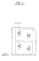
- the number of the primary boundaries existing on the active channel region depends on a grain size and a tilt angle " ⁇ " of a grain boundary and a dimension ( i . e ., length L and width W) of the active channel region, as illustrated in FIG. 1.
- the number of the primary grain boundaries existing on an arbitrary active channel region with the same channel length can be either "Nmax” or "Nmax -1".
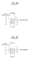
- the TFT of FIG. 2A has two primary boundaries, and the TFT of FIG. 2B has three primary boundaries.
- the display device As the TFTs having the same number of primary boundaries become more dominant, the display device having an excellent TFT characteristic uniformity can be achieved. However, when the TFTs having Nmax primary-boundaries and the TFTs having "Nmax-1" primary-boundaries are equal in number, the display device has a worst uniformity in TFT characteristics.
- the active channel region having large silicon grains can be formed using a sequential lateral solidification (SLS) technique.
- SLS sequential lateral solidification
- the TFT manufactured by employing such an active channel region shows similar characteristics to those of the TFT manufactured by using a single crystalline silicon.
- a display device includes millions of pixels.
- a liquid crystal display (LCD) device includes one TFT per one pixel, and an organic electroluminescent (EL) display device includes at least two TFTs per one pixel. Therefore, it is impossible to manufacture millions of TFTs that are all equal in number of the primary grain boundaries existing on the active channel region and in the grain growth direction.
- LCD liquid crystal display
- EL organic electroluminescent
- International Patent No. WO 97/45827 discloses a technique to form an active channel region having large silicon grains using the SLS technique.
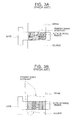
- An amorphous silicon layer is deposited using a PECVD technique, an LPCVD technique, or a sputtering technique. Thereafter, the entire portion or a selected portion of the amorphous silicon layer is crystallized using the SLS technique, as illustrated in FIGs. 3A and 3B.
- a laser beam or a stage can be stepped up or down, or shifted. Therefore, a misalignment between regions scanned by the laser beam occurs, resulting in a different number of primary grain boundaries in the active channel region from TFT to TFT.
- the position and dimension of TFTs are designed to control the number and position of the primary grain boundaries, which complicates both the TFT design and the fabrication process.
- the number of primary grain boundaries included in the active channel region of the individual TFTs can differ from each other, leading to bad uniformity in TFT characteristics.
- US Patent No. 6,177,391 discloses a method of manufacturing a TFT, wherein the active channel region of the TFT having large silicon grains is formed using the SLS technique.
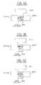
- a channel direction is parallel to a grain growth direction, as illustrated in FIG. 4A, a barrier effect of the grain boundary for a charge carrier direction is minimized, whereupon the TFT can have a characteristic similar to the single crystalline silicon.
- the grain boundaries act as a trap of the charge carriers, whereupon a characteristic of the TFT greatly deteriorates.
- the TFTs of which channel direction is perpendicular to a grain growth direction can be manufactured.
- a characteristic uniformity of the TFTs can be improved without greatly lowering the characteristics of the TFTs by tilting an angle of a channel direction to a grain growth direction by 30° to 60°.
- this method cannot remove the primary boundaries completely from the active channel region, and thus the nonuniformity in the TFT characteristics due to the differing number of the primary grain boundaries still exists.
- TFT thin film transistor
- a poly-silicon layer of a thin film transistor comprising an active channel region, wherein a length of the active channel region is an integer multiple of a grain size.
- a poly-silicon layer of a thin film transistor comprising an active channel region, wherein a probability that a maximum number of primary grain boundaries exists on the active channel region is defined as a ratio of the distance in which the length of the active channel in the longitudinal direction of grains minus a distance that a "maximum number - 1" of primary grain boundaries occupy, to the longitudinal length of the grains, and the probability is not 0.5.
- a probability P that Nmax primary boundaries exists on the active channel region is drawn as a function of a grain size, a tilt angle of the grain boundary, and a dimension of the active channel region.
- an angle " ⁇ " formed by the primary boundary and an imaginary normal line NN between the source and the drain electrodes is in a range between -45° and 45°. That is, "-45° ⁇ ⁇ ⁇ 45°" is valid.
- the distance D can be defined as a function of length L, width W, and tilt angle ⁇ .
- Nmax ⁇ (D/Gs).
- a probability Q that Nmax -1 primary boundaries exist on the active channel region can be defined as follows:
- the active channel region of the TFT has Nmax primary boundaries or Nmax -1 primary boundaries.
- the probability has the following meaning.
- Nmax primary boundaries exist on the active channel region is "0,” and thus, Nmax-1 primary boundaries exist on the active channel region.
- 0 ⁇ P ⁇ 0.5 a probability that Nmax primary boundaries exist on the active channel region is lower than a probability that Nmax - 1 primary boundaries exist on the active channel region.
- P 0.5: a probability that Nmax primary boundaries exist on the active channel region is equal to a probability that Nmax - 1 primary boundaries exist on the active channel region.
- 0.5 ⁇ P ⁇ 1 a probability that Nmax primary boundaries exist on the active channel region is higher than a probability that Nmax - 1 primary boundaries exist on the active channel region.
- Nmax primary boundaries exist on the active channel region is "1," and thus, the Nmax primary boundaries exist on the active channel region.
- the poly-silicon layers having a probability of "0" or "1,” for such a reason as, for example, due to a process margin during a wet or dry-etching of a gate metal. It is preferred that the poly-silicon layer is manufactured based on a probability of 0 ⁇ P ⁇ 0.25 or 0.75 ⁇ P ⁇ 1, which is a range of uniformity in the TFT characteristics required in the display device.
- the primary grain boundary is parallel to the imaginary normal line NN. That is, the tilt angle ⁇ of the primary grain boundary is "0°.” In this case, when the same number of primary grain boundaries exists on the active channel region, the effects of the secondary grain boundaries to the TFT characteristics are reduced in comparison to the case where the tilt angle ⁇ is not "0°,” and therefore it is understood that the TFT characteristics are improved.
- the length L is 9 ⁇ m, and a grain size Gs is 2 ⁇ m.
- Nmax is 5. Therefore, four or five primary grain boundaries exist on the active channel region of FIG. 9A. As a result, P and Q are 0.5, respectively. Therefore, it is understood that the uniformity of the TFT characteristics is worst.
- the length L is 9 ⁇ m, and a grain size Gs is 4 ⁇ m.
- Nmax is 3. Therefore, two or three primary grain boundaries exist on the active channel region of FIG. 9B.
- P and Q are 0.25 and 0.75, respectively. Therefore, it is understood that the uniformity of the TFT characteristics becomes improved in comparison to those having the active channel region of FIG. 9A.
- the length L is 10 ⁇ m, and a grain size Gs is 2 ⁇ m.
- Nmax is 5. Therefore, four or five primary grain boundaries exist on the active channel region of FIG. 10A.
- P and Q are 1 and 0, respectively. Therefore, it is understood that the uniformity of the TFT characteristics is optimal.
- the length L is 10 ⁇ m, and a grain size Gs is 4 ⁇ m.
- Nmax is 3. Therefore, two or three primary grain boundaries exist on the active channel region of FIG. 10B.
- P and Q are 0.5 and 0.5, respectively. Therefore, it is understood that the uniformity of the TFT characteristics becomes poor in comparison to those having the active channel region of FIG. 10A.
- the length L is 4 ⁇ m, and a grain size Gs is 8 ⁇ m.
- Nmax is 1. Therefore, one or no grain boundaries exist on the active channel region of FIG. 1A.
- P and Q are 0.5, respectively. Therefore, it is understood that the uniformity of the TFT characteristics is worst.
- the length L is 4 ⁇ m, and a grain size Gs is 16 ⁇ m.
- Nmax is 1. Therefore, one or no primary grain boundaries exist on the active channel region of FIG. 11B.
- P and Q are 0.25 and 0.75, respectively. Therefore, it is understood that the uniformity of the TFT characteristics becomes improved in comparison to those having the active channel region of FIG. 11A.
- the characteristic uniformity of the TFTs can be predicted by obtaining the probability that the primary grain boundaries exist on the active channel region. Therefore, process parameters of a silicon crystallization process are set to achieve the TFTs having an excellent uniformity.
- Tables 1 to 4 illustrate the probability P according to a grain size and a dimension of the active channel region.
- the width W is 10 ⁇ m.
- the tilt angle ⁇ is 0°. It is understood that when a ratio of the length of the active channel region with respect to the maximum number of the primary boundaries is equal to a grain size, the probability P is 1. 0 L( ⁇ m) Gs( ⁇ m) Nmax P L( ⁇ m) Gs( ⁇ m) Nmax P L( ⁇ m) Gs( ⁇ m) Nmax P 0° 4 0.5 8 1.000 7 0.5 14 1.000 10 0.5 20 1.000 1 4 1.000 1 7 1.000 1 10 1.000 1.5 3 0.667 1.5 5 0.667 1.5 7 0.667 2 2 1.000 2 4 0.500 2 5 1.000 2.5 2 0.600 2.5 3 0.800 2.5 4 1.000 3 2 0.333 3 3 0.333 3 4 0.333 3.5 2 0.143 3.5 2 1.000 3.5 3 0.857 4 1 1.000 4 2 0.750 4 3 0.500 4.5 1 0.889 4.5 2 0.556 4.5 3 0.222 5 1 0.800 5 2 0.400 5 2 1.000 5.5 1 0.727 5.5 2 0.273 5.5 2 0.818
- the tilt angle ⁇ is 0°. It is understood that when the maximum number of the primary boundaries is equal to the length of the active channel divided by the grain size, the probability P is 1.
- the TFTs having uniform characteristics can be manufactured by setting parameters such as a grain size, a tilt angle of a grain boundary, and a dimension of an active channel region according to the probability.
Landscapes
- Thin Film Transistor (AREA)
- Liquid Crystal (AREA)
- Recrystallisation Techniques (AREA)
Abstract
Description
"D = (L + W·tan) × cos = L·cos + W·tan·cos" is valid. Since "tan·cos" is "sin", "D" is "L·cos + W·sin".
| • | Gs(µm) | L(µm) | Nmax | P | Gs(µm) | L(µm) | Nmax | P | Gs(µm) | L(µm) | Nmax | P |
| 2° | 0.4 | 1 | 3 | 0.778 | 1.5 | 1 | 1 | 0.741 | 2.5 | 1 | 1 | 0.444 |
| 2 | 6 | 0.277 | 2 | 2 | 0.407 | 2 | 1 | 0.844 | ||||
| 3 | 8 | 0.777 | 3 | 3 | 0.074 | 3 | 2 | 0.244 | ||||
| 4 | 11 | 0.277 | 4 | 3 | 0.741 | 4 | 2 | 0.644 | ||||
| 5 | 13 | 0.778 | 5 | 4 | 0.407 | 5 | 3 | 0.044 | ||||
| 6 | 16 | 0.277 | 6 | 5 | 0.074 | 6 | 3 | 0.444 | ||||
| 7 | 18 | 0.777 | 7 | 5 | 0.740 | 7 | 3 | 0.844 | ||||
| 8 | 21 | 0.277 | 8 | 6 | 0.407 | 8 | 4 | 0.244 | ||||
| 9 | 23 | 0.776 | 9 | 7 | 0.074 | 9 | 4 | 0.644 | ||||
| 10 | 26 | 0.276 | 10 | 7 | 0.740 | 10 | 5 | 0.044 | ||||
| 5° | 0.4 4 | 1 | 4 | 0.193 | 1.5 | 1 | 1 | 0.852 | 2.5 | 1 | 1 | 0.511 |
| 2 | 6 | 0.692 | 2 | 2 | 0.518 | 2 | 1 | 0.911 | ||||
| 3 | 9 | 0.191 | 3 | 3 | 0.184 | 3 | 2 | 0.311 | ||||
| 4 | 11 | 0.690 | 4 | 3 | 0.851 | 4 | 2 | 0.710 | ||||
| 5 | 14 | 0.190 | 5 | 4 | 0.517 | 5 | 3 | 0.110 | ||||
| 6 | 16 | 0.689 | 6 | 5 | 0.184 | 6 | 3 | 0.510 | ||||
| 7 | 19 | 0.188 | 7 | 5 | 0.850 | 7 | 3 | 0.910 | ||||
| 8 | 21 | 0.687 | 8 | 6 | 0.516 | 8 | 4 | 0.310 | ||||
| 9 | 24 | 0.186 | 9 | 7 | 0.183 | 9 | 4 | 0.710 | ||||
| 10 | 26 | 0.685 | 19 | 7 | 0.849 | 10 | 5 | 0.110 |
| | L(µm) | Gs(µm) | Nmax | P | L(µm) | Gs(µm) | Nmax | P | L(µm) | Gs(µm) | Nmax | P |
| 2° | 4 | 0.5 | 9 | 0.222 | 7 | 0.5 | 15 | 0.221 | 2.5 | 0.5 | 21 | 0.221 |
| 1 | 5 | 0.111 | 1 | 8 | 0.111 | 1 | 11 | 0.110 | ||||
| 1.5 | 3 | 0.741 | 1.5 | 5 | 0.740 | 1.5 | 7 | 0.740 | ||||
| 2 | 3 | 0.055 | 2 | 4 | 0.555 | 2 | 6 | 0.055 | ||||
| 2.5 | 2 | 0.644 | 2.5 | 3 | 0.844 | 2.5 | 5 | 0.044 | ||||
| 3 | 2 | 0.370 | 3 | 3 | 0.370 | 3 | 4 | 0.370 | ||||
| 3.5 | 2 | 0.175 | 3.5 | 3 | 0.032 | 3.5 | 4 | 0.889 | ||||
| 4 | 2 | 0.028 | 4 | 2 | 0.778 | 4 | 3 | 0.528 | ||||
| 4.5 | 1 | 0.914 | 4.5 | 2 | 0.580 | 4.5 | 3 | 0.247 | ||||
| 5 | 1 | 0.822 | 5 | 2 | 0.422 | 5 | 3 | 0.022 | ||||
| 5° | 4 | 0.5 | 9 | 0.552 | 7 | 0.5 | 15 | 0.550 | 2.5 | 0.5 | 21 | 0.548 |
| 1 | 5 | 0.276 | 1 | 8 | 0.275 | 1 | 11 | 0.274 | ||||
| 1.5 | 3 | 0.851 | 1.5 | 5 | 0.850 | 1.5 | 7 | 0.849 | ||||
| 2 | 3 | 0.138 | 2 | 4 | 0.638 | 2 | 6 | 0.137 | ||||
| 2.5 | 2 | 0.710 | 2.5 | 3 | 0.910 | 2.5 | 5 | 0.110 | ||||
| 3 | 2 | 0.425 | 3 | 3 | 0.425 | 3 | 4 | 0.425 | ||||
| 3.5 | 2 | 0.222 | 3.5 | 3 | 0.079 | 3.5 | 4 | 0.935 | ||||
| 4 | 2 | 0.069 | 4 | 2 | 0.819 | 4 | 3 | 0.568 | ||||
| 4.5 | 1 | 0.950 | 4.5 | 2 | 0.617 | 4.5 | 3 | 0.283 | ||||
| 5 | 1 | 0.855 | 5 | 2 | 0.455 | 5 | 3 | 0.055 |
| Gs(µm) | L(µm) | Nmax | P | Gs(µm) | L(µm) | Nmax | P | Gs(µm) | L(µm) | Nmax | P | |
| 0° | 0.4 | 1 | 3 | 0.500 | 1.5 | 1 | 1 | 0.667 | 2.5 | 1 | 1 | 0.400 |
| 2 | 5 | 1.000 | 2 | 2 | 0.333 | 2 | 1 | 0.800 | ||||
| 3 | 8 | 0.500 | 3 | 2 | 1.000 | 3 | 2 | 0.200 | ||||
| 4 | 10 | 1.000 | 4 | 3 | 0.667 | 4 | 2 | 0.600 | ||||
| 5 | 13 | 0.500 | 5 | 4 | 0.333 | 5 | 2 | 1.000 | ||||
| 6 | 15 | 1.000 | 6 | 4 | 1.000 | 6 | 3 | 0.400 | ||||
| 7 | 18 | 0.500 | 7 | 5 | 0.667 | 7 | 3 | 0.800 | ||||
| 8 | 20 | 1.000 | 8 | 6 | 0.333 | 8 | 4 | 0.200 | ||||
| 9 | 23 | 0.500 | 9 | 6 | 1.000 | 9 | 4 | 0.600 | ||||
| 10 | 25 | 1.000 | 10 | 7 | 0.667 | 10 | 4 | 1.000 | ||||
| 11 | 28 | 0.500 | 11 | 8 | 0.333 | 11 | 5 | 0.400 | ||||
| 12 | 30 | 1.000 | 12 | 8 | 1.000 | 12 | 5 | 0.800 | ||||
| 13 | 33 | 0.500 | 13 | 9 | 0.667 | 13 | 6 | 0.200 | ||||
| 14 | 35 | 1.000 | 14 | 10 | 0.333 | 14 | 6 | 0.600 | ||||
| 15 | 38 | 0.500 | 15 | 10 | 1.000 | 15 | 6 | 1.000 | ||||
| 16 | 40 | 1.000 | 16 | 11 | 0.667 | 16 | 7 | 0.400 | ||||
| 17 | 43 | 0.500 | 17 | 12 | 0.333 | 17 | 7 | 0.800 | ||||
| 18 | 45 | 1.000 | 18 | 12 | 1.000 | 18 | 8 | 0.200 | ||||
| 19 | 48 | 0.500 | 19 | 13 | 0.667 | 19 | 8 | 0.600 | ||||
| 20 | 50 | 1.000 | 20 | 14 | 0.333 | 20 | 8 | 1.000 |
| 0 | L(µm) | Gs(µm) | Nmax | P | L(µm) | Gs(µm) | Nmax | P | L(µm) | Gs(µm) | Nmax | P |
| 0° | 4 | 0.5 | 8 | 1.000 | 7 | 0.5 | 14 | 1.000 | 10 | 0.5 | 20 | 1.000 |
| 1 | 4 | 1.000 | 1 | 7 | 1.000 | 1 | 10 | 1.000 | ||||
| 1.5 | 3 | 0.667 | 1.5 | 5 | 0.667 | 1.5 | 7 | 0.667 | ||||
| 2 | 2 | 1.000 | 2 | 4 | 0.500 | 2 | 5 | 1.000 | ||||
| 2.5 | 2 | 0.600 | 2.5 | 3 | 0.800 | 2.5 | 4 | 1.000 | ||||
| 3 | 2 | 0.333 | 3 | 3 | 0.333 | 3 | 4 | 0.333 | ||||
| 3.5 | 2 | 0.143 | 3.5 | 2 | 1.000 | 3.5 | 3 | 0.857 | ||||
| 4 | 1 | 1.000 | 4 | 2 | 0.750 | 4 | 3 | 0.500 | ||||
| 4.5 | 1 | 0.889 | 4.5 | 2 | 0.556 | 4.5 | 3 | 0.222 | ||||
| 5 | 1 | 0.800 | 5 | 2 | 0.400 | 5 | 2 | 1.000 | ||||
| 5.5 | 1 | 0.727 | 5.5 | 2 | 0.273 | 5.5 | 2 | 0.818 | ||||
| 6 | 1 | 0.667 | 6 | 2 | 0.167 | 6 | 2 | 0.667 | ||||
| 6.5 | 1 | 0.615 | 6.5 | 2 | 0.077 | 6.5 | 2 | 0.538 | ||||
| 7 | 1 | 0.571 | 7 | 1 | 1.000 | 7 | 2 | 0.429 | ||||
| 7.5 | 1 | 0.533 | 7.5 | 1 | 0.933 | 7.5 | 2 | 0.333 | ||||
| 8 | 1 | 0.500 | 8 | 1 | 0.875 | 8 | 2 | 0.250 | ||||
| 8.5 | 1 | 0.471 | 8.5 | 1 | 0.824 | 8.5 | 2 | 0.176 | ||||
| 9 | 1 | 0.444 | 9 | 1 | 0.778 | 9 | 2 | 0.111 | ||||
| 9.5 | 1 | 0.421 | 9.5 | 1 | 0.737 | 9.5 | 2 | 0.053 | ||||
| 10 | 1 | 0.400 | 10 | 1 | 0.700 | 10 | 1 | 1.000 |
Claims (36)
- A poly-silicon layer of a thin film transistor (TFT), comprising:wherein a probability P that a maximum number of primary grain boundaries exists on the active channel region is not 0.5, the probability P obtained by the following equation:an active channel region,
- The poly-silicon layer according to claim 1, wherein the poly-silicon layer is used in a TFT arranged in a display region.
- The poly-silicon layer according to claim 1, wherein the poly-silicon layer is used in a TFT arranged in a driving circuit portion.
- The poly-silicon layer according to claim 1, where P is more than 0.75 or less than 0.25.
- The poly-silicon layer according to claim 1, wherein is -45° ≤ ≤ 45°.
- The poly-silicon layer according to claim 1, wherein the grain size is more than 0.2 µm.
- The poly-silicon layer according to claim 1, wherein the number of grains is two or more.
- The poly-silicon layer according to claim 1, wherein a probability Q that (Nmax - 1) primary grain boundaries exist on the active channel region is defined: Q = 1 - P.
- The poly-silicon layer according to claim 1, wherein Nmax = ξ(D/Gs), where ξ (x) is the smallest integer among numbers ≥ x, and "x" is an arbitrary number.
- The poly-silicon layer according to claim 1, wherein Nmax is one of 1 to 10.
- The poly-silicon layer according to claim 1, wherein when is 0°, a ratio of the length of the active channel region with respect to Nmax is equal to the grain size.
- The poly-silicon layer according to claim 1, wherein when is 0°, the length of the active channel region is equal to the grain size by Nmax.
- A poly-silicon layer of a thin film transistor (TFT), comprising:wherein a length of the active channel region is an integer multiple of a grain size.an active channel region,
- The poly-silicon layer according to claim 13, wherein the poly-silicon layer is used in a TFT arranged in a display region.
- The poly-silicon layer according to claim 13, wherein the poly-silicon layer is used in a TFT arranged in a driving circuit portion.
- The poly-silicon layer according to claim 13, wherein the length of the active channel region is more than 2 µm.
- The poly-silicon layer according to claim 13, wherein the number of grains is two or more.
- The poly-silicon layer according to claim 13, wherein a grain size is more than 2 µm.
- A poly-silicon layer of a thin film transistor (TFT), comprising:wherein a probability that a maximum number of primary grain boundaries exists on the active channel region is defined as a ratio of the distance in which the length of the active channel in the logitudinal direction of grains minus a distance that a "maximum number - 1" primary grain boundaries occupy, to the longitudinal length of the grains, and the probability is not 0.5.an active channel region,
- The poly-silicon layer according to claim 19, wherein the poly-silicon layer is used in a TFT arranged in a display region.
- The poly-silicon layer according to claim 19, wherein the poly-silicon layer is used in a TFT arranged in a driving circuit portion.
- The poly-silicon layer according to claim 19, where P is more than 0.75 or less than 0.25.
- The poly-silicon layer according to claim 19, wherein a length of the active channel region is an ingeter multiple of a grain size.
- The poly-silicon layer according to claim 19, wherein a grain grows in a constant direction.
- The poly-silicon layer according to claim 19, wherein a grain size is more than 2 µm.
- The poly-silicon layer according to claim 19, wherein a maximum number of the grain boundaries is one of 1 to 10.
- The poly-silicon layer according to claim 19, wherein the length of the active channel region is more than 2 µm.
- The poly-silicon layer according to claim 18, wherein the number of grains is two or more.
- A device comprising:wherein a probability P that a maximum number of primary grain boundaries exists on the active channel region is not 0.5, the probability P obtained by the following equation:a thin film transistor having a poly-silicon layer, wherein said poly-silicon layer includes an active channel region,
- The device according to claim 29, wherein said device is a display device or a semiconductor device.
- The device according to claim 30, wherein said display device comprises one of a liquid display (LCD) device and an organic EL display device.
- A display device having multiple TFTs, comprising:wherein the TFTs are manufactured by setting parameters of grain size, a tilt angle of a grain boundary, and a dimension of the active channel region.a TFT having a poly-silicon layer with an active channel region having at least one primary boundary associated therewith, such that primary boundaries with a same number for the active channel region as compared with the other multiple TFTs of the display device is dominant throughout the display device;
- The display device according to claim 32, wherein the percentage of primary boundaries among the display device with the same number of boundaries is more than 75%.
- The display device according to claim 32, wherein a maximum number of grain boundaries is between 1 to 10.
- The display device according to claim 32, wherein the grain size is more than 0.2 µm.
- The display device according to claim 32, wherein the number of grains is two or more.
Applications Claiming Priority (2)
| Application Number | Priority Date | Filing Date | Title |
|---|---|---|---|
| KR2001074375 | 2001-11-27 | ||
| KR10-2001-0074375A KR100483985B1 (en) | 2001-11-27 | 2001-11-27 | Polysilicon thin layer for thin film transistor and device using thereof |
Publications (3)
| Publication Number | Publication Date |
|---|---|
| EP1317002A2 true EP1317002A2 (en) | 2003-06-04 |
| EP1317002A3 EP1317002A3 (en) | 2004-09-29 |
| EP1317002B1 EP1317002B1 (en) | 2016-10-12 |
Family
ID=19716364
Family Applications (1)
| Application Number | Title | Priority Date | Filing Date |
|---|---|---|---|
| EP02090384.5A Expired - Lifetime EP1317002B1 (en) | 2001-11-27 | 2002-11-20 | Display device having polysilicon layer providing thin film transistors |
Country Status (5)
| Country | Link |
|---|---|
| US (1) | US6759679B2 (en) |
| EP (1) | EP1317002B1 (en) |
| JP (1) | JP4361722B2 (en) |
| KR (1) | KR100483985B1 (en) |
| CN (3) | CN100511710C (en) |
Cited By (1)
| Publication number | Priority date | Publication date | Assignee | Title |
|---|---|---|---|---|
| EP1860699A1 (en) * | 2006-05-25 | 2007-11-28 | Sony Corporation | Display having thin fim transistors with channel region of varying crystal state |
Families Citing this family (18)
| Publication number | Priority date | Publication date | Assignee | Title |
|---|---|---|---|---|
| KR100514179B1 (en) * | 2002-11-19 | 2005-09-13 | 삼성에스디아이 주식회사 | Thin film transistor and electorluminescent display device using thereof |
| KR100483987B1 (en) * | 2002-07-08 | 2005-04-15 | 삼성에스디아이 주식회사 | Polysilicon thin layer for thin film transistor and device using thereof |
| KR100454751B1 (en) * | 2002-10-21 | 2004-11-03 | 삼성에스디아이 주식회사 | Method for fabricating thin film transistor using dual or multiple gates |
| CN1324540C (en) | 2003-06-05 | 2007-07-04 | 三星Sdi株式会社 | Flat panel display device with polysilicon thin film transistor |
| KR100521274B1 (en) * | 2003-06-10 | 2005-10-12 | 삼성에스디아이 주식회사 | Cmos thin film transistor and display device using the same |
| US7858450B2 (en) * | 2004-01-06 | 2010-12-28 | Samsung Electronics Co., Ltd. | Optic mask and manufacturing method of thin film transistor array panel using the same |
| KR101034744B1 (en) * | 2004-06-25 | 2011-05-17 | 엘지디스플레이 주식회사 | Thin film transistor structure of liquid crystal display device |
| KR100712101B1 (en) * | 2004-06-30 | 2007-05-02 | 삼성에스디아이 주식회사 | Thin film transistor and its manufacturing method |
| KR20100036624A (en) * | 2008-09-30 | 2010-04-08 | 삼성전자주식회사 | Thin film transistor substrate and organic light emitting display having the same |
| WO2013078641A1 (en) * | 2011-11-30 | 2013-06-06 | 广东中显科技有限公司 | Bridge die polysilicon thin-film transistor and manufacturing method thereof |
| CN103137484A (en) * | 2011-11-30 | 2013-06-05 | 广东中显科技有限公司 | Production method of bridging grain polycrystalline silicon thin film transistor |
| CN104900532B (en) | 2015-06-15 | 2018-10-02 | 京东方科技集团股份有限公司 | A kind of thin film transistor (TFT) and preparation method thereof, array substrate, display device |
| JP6434872B2 (en) * | 2015-07-31 | 2018-12-05 | 東芝メモリ株式会社 | Semiconductor device |
| US10629752B1 (en) * | 2018-10-11 | 2020-04-21 | Applied Materials, Inc. | Gate all-around device |
| US11024736B2 (en) | 2019-08-09 | 2021-06-01 | Micron Technology, Inc. | Transistor and methods of forming integrated circuitry |
| WO2021030127A1 (en) * | 2019-08-09 | 2021-02-18 | Micron Technology, Inc. | Transistor and methods of forming transistors |
| US10964811B2 (en) | 2019-08-09 | 2021-03-30 | Micron Technology, Inc. | Transistor and methods of forming transistors |
| US11637175B2 (en) | 2020-12-09 | 2023-04-25 | Micron Technology, Inc. | Vertical transistors |
Family Cites Families (19)
| Publication number | Priority date | Publication date | Assignee | Title |
|---|---|---|---|---|
| US5498904A (en) * | 1994-02-22 | 1996-03-12 | Sanyo Electric Co., Ltd. | Polycrystalline semiconductive film, semiconductor device using the same and method of manufacturing the same |
| JPH07335906A (en) * | 1994-06-14 | 1995-12-22 | Semiconductor Energy Lab Co Ltd | Thin film semiconductor device and manufacturing method thereof |
| JPH1065180A (en) * | 1996-03-29 | 1998-03-06 | A G Technol Kk | Polycrystalline semiconductor thin film and forming method thereof, polycrystalline semiconductor tft, and tft substrate |
| JP3204986B2 (en) * | 1996-05-28 | 2001-09-04 | ザ トラスティース オブ コロンビア ユニヴァーシティ イン ザ シティ オブ ニューヨーク | Crystallization of semiconductor film region on substrate and device manufactured by this method |
| US5981974A (en) * | 1996-09-30 | 1999-11-09 | Sharp Kabushiki Kaisha | Semiconductor device and method for fabricating the same |
| SE511133C2 (en) * | 1996-11-07 | 1999-08-09 | Dresser Wayne Ab | Method and device for volume determination |
| WO1998057372A1 (en) * | 1997-06-10 | 1998-12-17 | The Board Of Trustees Of The Leland Stanford Junior University | LATERALLY CRYSTALLIZED TFTs AND METHODS FOR MAKING LATERALLY CRYSTALLIZED TFTs |
| JP3642546B2 (en) * | 1997-08-12 | 2005-04-27 | 株式会社東芝 | Method for producing polycrystalline semiconductor thin film |
| JPH11168216A (en) * | 1997-12-04 | 1999-06-22 | Matsushita Electron Corp | Thin film transistor and method of manufacturing the same |
| JPH11219133A (en) * | 1998-02-02 | 1999-08-10 | Tdk Corp | Image display device |
| KR100292048B1 (en) * | 1998-06-09 | 2001-07-12 | 구본준, 론 위라하디락사 | Manufacturing Method of Thin Film Transistor Liquid Crystal Display |
| US6479837B1 (en) * | 1998-07-06 | 2002-11-12 | Matsushita Electric Industrial Co., Ltd. | Thin film transistor and liquid crystal display unit |
| JP2000133807A (en) * | 1998-10-22 | 2000-05-12 | Seiko Epson Corp | Polycrystalline silicon thin film transistor |
| US6177391B1 (en) * | 1999-05-27 | 2001-01-23 | Alam Zafar | One time use disposable soap and method of making |
| KR100303142B1 (en) * | 1999-10-29 | 2001-11-02 | 구본준, 론 위라하디락사 | Fabricating method of liquid crystal display pannel |
| JP2001135825A (en) * | 1999-11-09 | 2001-05-18 | Seiko Epson Corp | Device simulation method |
| CN1217417C (en) * | 1999-12-10 | 2005-08-31 | 株式会社半导体能源研究所 | Semiconductor device and manufacturing method thereof |
| JP4732599B2 (en) * | 2001-01-26 | 2011-07-27 | 株式会社日立製作所 | Thin film transistor device |
| US6426246B1 (en) * | 2001-02-21 | 2002-07-30 | United Microelectronics Corp. | Method for forming thin film transistor with lateral crystallization |
-
2001
- 2001-11-27 KR KR10-2001-0074375A patent/KR100483985B1/en not_active Expired - Lifetime
-
2002
- 2002-06-19 US US10/173,977 patent/US6759679B2/en not_active Expired - Lifetime
- 2002-11-20 EP EP02090384.5A patent/EP1317002B1/en not_active Expired - Lifetime
- 2002-11-21 JP JP2002338473A patent/JP4361722B2/en not_active Expired - Lifetime
- 2002-11-27 CN CNB021524327A patent/CN100511710C/en not_active Expired - Lifetime
- 2002-11-27 CN CN2009101262299A patent/CN101494235B/en not_active Expired - Lifetime
- 2002-11-27 CN CN2010106179144A patent/CN102142463A/en active Pending
Cited By (2)
| Publication number | Priority date | Publication date | Assignee | Title |
|---|---|---|---|---|
| EP1860699A1 (en) * | 2006-05-25 | 2007-11-28 | Sony Corporation | Display having thin fim transistors with channel region of varying crystal state |
| US7541615B2 (en) | 2006-05-25 | 2009-06-02 | Sony Corporation | Display device including thin film transistors |
Also Published As
| Publication number | Publication date |
|---|---|
| JP4361722B2 (en) | 2009-11-11 |
| US6759679B2 (en) | 2004-07-06 |
| CN101494235B (en) | 2011-03-23 |
| CN1421935A (en) | 2003-06-04 |
| KR100483985B1 (en) | 2005-04-15 |
| CN100511710C (en) | 2009-07-08 |
| CN101494235A (en) | 2009-07-29 |
| EP1317002A3 (en) | 2004-09-29 |
| KR20030043292A (en) | 2003-06-02 |
| CN102142463A (en) | 2011-08-03 |
| EP1317002B1 (en) | 2016-10-12 |
| US20030102508A1 (en) | 2003-06-05 |
| JP2003188188A (en) | 2003-07-04 |
Similar Documents
| Publication | Publication Date | Title |
|---|---|---|
| US6759679B2 (en) | Poly-silicon layer of a thin film transistor and display device having the same | |
| US8987120B2 (en) | Flat panel display device comprising polysilicon thin film transistor and method of manufacturing the same | |
| US8097883B2 (en) | Thin film transistors in pixel and driver portions characterized by surface roughness | |
| US20030141503A1 (en) | Polycrystalline silicon thin film for a thin film transistor and display device using the same | |
| US20060157711A1 (en) | Thin film transistor array panel | |
| US20040038438A1 (en) | Method for reducing surface roughness of polysilicon films for liquid crystal displays | |
| US5733793A (en) | Process formation of a thin film transistor | |
| JP2007158290A (en) | Organic light emitting diode (OLED) display panel and method for forming a polysilicon channel layer thereof | |
| US8314428B2 (en) | Thin film transistor with LDD/offset structure | |
| EP1381089A2 (en) | Polycrystalline silicon thin film used in a thin film transistor and a device using the same | |
| EP1414062A2 (en) | Method of fabricating a thin film transistor using dual or multiple gates | |
| KR100552958B1 (en) | Flat panel display device including polycrystalline silicon thin film transistor and manufacturing method thereof | |
| EP1422760A2 (en) | Thin film transistors and organic electroluminescent device using the same | |
| US7750348B2 (en) | Display device having crystal grain boundaries providing superior driving and luminance characteristics | |
| US20040163585A1 (en) | Method for manufacturing polycrystalline silicon thin film and thin film transistor fabricated using polycrystalline silicon thin film manufactured by the manufacturing | |
| US7776669B2 (en) | Thin film transistor and method of fabricating the same | |
| US7026201B2 (en) | Method for forming polycrystalline silicon thin film transistor | |
| KR100542991B1 (en) | Flat panel display device including polycrystalline silicon thin film transistor |
Legal Events
| Date | Code | Title | Description |
|---|---|---|---|
| PUAI | Public reference made under article 153(3) epc to a published international application that has entered the european phase |
Free format text: ORIGINAL CODE: 0009012 |
|
| AK | Designated contracting states |
Designated state(s): AT BE BG CH CY CZ DE DK EE ES FI FR GB GR IE IT LI LU MC NL PT SE SK TR |
|
| AX | Request for extension of the european patent |
Extension state: AL LT LV MK RO SI |
|
| PUAL | Search report despatched |
Free format text: ORIGINAL CODE: 0009013 |
|
| AK | Designated contracting states |
Kind code of ref document: A3 Designated state(s): AT BE BG CH CY CZ DE DK EE ES FI FR GB GR IE IT LI LU MC NL PT SE SK TR |
|
| AX | Request for extension of the european patent |
Extension state: AL LT LV MK RO SI |
|
| 17P | Request for examination filed |
Effective date: 20041118 |
|
| 17Q | First examination report despatched |
Effective date: 20050322 |
|
| AKX | Designation fees paid |
Designated state(s): AT BE BG CH CY CZ DE DK EE ES FI FR GB GR IE IT LI LU MC NL PT SE SK TR |
|
| 17Q | First examination report despatched |
Effective date: 20050322 |
|
| RAP1 | Party data changed (applicant data changed or rights of an application transferred) |
Owner name: SAMSUNG MOBILE DISPLAY CO., LTD. |
|
| RAP1 | Party data changed (applicant data changed or rights of an application transferred) |
Owner name: SAMSUNG DISPLAY CO., LTD. |
|
| RAP1 | Party data changed (applicant data changed or rights of an application transferred) |
Owner name: SAMSUNG DISPLAY CO., LTD. |
|
| REG | Reference to a national code |
Ref country code: DE Ref legal event code: R079 Ref document number: 60248403 Country of ref document: DE Free format text: PREVIOUS MAIN CLASS: H01L0029786000 Ipc: H01L0027120000 |
|
| GRAP | Despatch of communication of intention to grant a patent |
Free format text: ORIGINAL CODE: EPIDOSNIGR1 |
|
| RIC1 | Information provided on ipc code assigned before grant |
Ipc: H01L 29/786 20060101ALI20160414BHEP Ipc: H01L 27/12 20060101AFI20160414BHEP |
|
| INTG | Intention to grant announced |
Effective date: 20160502 |
|
| GRAS | Grant fee paid |
Free format text: ORIGINAL CODE: EPIDOSNIGR3 |
|
| GRAA | (expected) grant |
Free format text: ORIGINAL CODE: 0009210 |
|
| AK | Designated contracting states |
Kind code of ref document: B1 Designated state(s): AT BE BG CH CY CZ DE DK EE ES FI FR GB GR IE IT LI LU MC NL PT SE SK TR |
|
| REG | Reference to a national code |
Ref country code: GB Ref legal event code: FG4D |
|
| REG | Reference to a national code |
Ref country code: CH Ref legal event code: EP |
|
| REG | Reference to a national code |
Ref country code: AT Ref legal event code: REF Ref document number: 837183 Country of ref document: AT Kind code of ref document: T Effective date: 20161015 |
|
| REG | Reference to a national code |
Ref country code: IE Ref legal event code: FG4D |
|
| REG | Reference to a national code |
Ref country code: DE Ref legal event code: R096 Ref document number: 60248403 Country of ref document: DE |
|
| REG | Reference to a national code |
Ref country code: FR Ref legal event code: PLFP Year of fee payment: 15 |
|
| REG | Reference to a national code |
Ref country code: NL Ref legal event code: MP Effective date: 20161012 |
|
| PG25 | Lapsed in a contracting state [announced via postgrant information from national office to epo] |
Ref country code: BE Free format text: LAPSE BECAUSE OF NON-PAYMENT OF DUE FEES Effective date: 20161130 |
|
| REG | Reference to a national code |
Ref country code: AT Ref legal event code: MK05 Ref document number: 837183 Country of ref document: AT Kind code of ref document: T Effective date: 20161012 |
|
| PG25 | Lapsed in a contracting state [announced via postgrant information from national office to epo] |
Ref country code: SE Free format text: LAPSE BECAUSE OF FAILURE TO SUBMIT A TRANSLATION OF THE DESCRIPTION OR TO PAY THE FEE WITHIN THE PRESCRIBED TIME-LIMIT Effective date: 20161012 Ref country code: GR Free format text: LAPSE BECAUSE OF FAILURE TO SUBMIT A TRANSLATION OF THE DESCRIPTION OR TO PAY THE FEE WITHIN THE PRESCRIBED TIME-LIMIT Effective date: 20170113 |
|
| PG25 | Lapsed in a contracting state [announced via postgrant information from national office to epo] |
Ref country code: PT Free format text: LAPSE BECAUSE OF FAILURE TO SUBMIT A TRANSLATION OF THE DESCRIPTION OR TO PAY THE FEE WITHIN THE PRESCRIBED TIME-LIMIT Effective date: 20170213 Ref country code: AT Free format text: LAPSE BECAUSE OF FAILURE TO SUBMIT A TRANSLATION OF THE DESCRIPTION OR TO PAY THE FEE WITHIN THE PRESCRIBED TIME-LIMIT Effective date: 20161012 Ref country code: ES Free format text: LAPSE BECAUSE OF FAILURE TO SUBMIT A TRANSLATION OF THE DESCRIPTION OR TO PAY THE FEE WITHIN THE PRESCRIBED TIME-LIMIT Effective date: 20161012 Ref country code: BE Free format text: LAPSE BECAUSE OF FAILURE TO SUBMIT A TRANSLATION OF THE DESCRIPTION OR TO PAY THE FEE WITHIN THE PRESCRIBED TIME-LIMIT Effective date: 20161012 Ref country code: NL Free format text: LAPSE BECAUSE OF FAILURE TO SUBMIT A TRANSLATION OF THE DESCRIPTION OR TO PAY THE FEE WITHIN THE PRESCRIBED TIME-LIMIT Effective date: 20161012 Ref country code: FI Free format text: LAPSE BECAUSE OF FAILURE TO SUBMIT A TRANSLATION OF THE DESCRIPTION OR TO PAY THE FEE WITHIN THE PRESCRIBED TIME-LIMIT Effective date: 20161012 |
|
| REG | Reference to a national code |
Ref country code: CH Ref legal event code: PL |
|
| REG | Reference to a national code |
Ref country code: DE Ref legal event code: R097 Ref document number: 60248403 Country of ref document: DE |
|
| PG25 | Lapsed in a contracting state [announced via postgrant information from national office to epo] |
Ref country code: DK Free format text: LAPSE BECAUSE OF FAILURE TO SUBMIT A TRANSLATION OF THE DESCRIPTION OR TO PAY THE FEE WITHIN THE PRESCRIBED TIME-LIMIT Effective date: 20161012 Ref country code: EE Free format text: LAPSE BECAUSE OF FAILURE TO SUBMIT A TRANSLATION OF THE DESCRIPTION OR TO PAY THE FEE WITHIN THE PRESCRIBED TIME-LIMIT Effective date: 20161012 Ref country code: SK Free format text: LAPSE BECAUSE OF FAILURE TO SUBMIT A TRANSLATION OF THE DESCRIPTION OR TO PAY THE FEE WITHIN THE PRESCRIBED TIME-LIMIT Effective date: 20161012 Ref country code: CZ Free format text: LAPSE BECAUSE OF FAILURE TO SUBMIT A TRANSLATION OF THE DESCRIPTION OR TO PAY THE FEE WITHIN THE PRESCRIBED TIME-LIMIT Effective date: 20161012 Ref country code: LI Free format text: LAPSE BECAUSE OF NON-PAYMENT OF DUE FEES Effective date: 20161130 Ref country code: CH Free format text: LAPSE BECAUSE OF NON-PAYMENT OF DUE FEES Effective date: 20161130 Ref country code: MC Free format text: LAPSE BECAUSE OF FAILURE TO SUBMIT A TRANSLATION OF THE DESCRIPTION OR TO PAY THE FEE WITHIN THE PRESCRIBED TIME-LIMIT Effective date: 20161012 |
|
| PLBE | No opposition filed within time limit |
Free format text: ORIGINAL CODE: 0009261 |
|
| STAA | Information on the status of an ep patent application or granted ep patent |
Free format text: STATUS: NO OPPOSITION FILED WITHIN TIME LIMIT |
|
| REG | Reference to a national code |
Ref country code: IE Ref legal event code: MM4A |
|
| PG25 | Lapsed in a contracting state [announced via postgrant information from national office to epo] |
Ref country code: BG Free format text: LAPSE BECAUSE OF FAILURE TO SUBMIT A TRANSLATION OF THE DESCRIPTION OR TO PAY THE FEE WITHIN THE PRESCRIBED TIME-LIMIT Effective date: 20170112 Ref country code: IT Free format text: LAPSE BECAUSE OF FAILURE TO SUBMIT A TRANSLATION OF THE DESCRIPTION OR TO PAY THE FEE WITHIN THE PRESCRIBED TIME-LIMIT Effective date: 20161012 |
|
| 26N | No opposition filed |
Effective date: 20170713 |
|
| PG25 | Lapsed in a contracting state [announced via postgrant information from national office to epo] |
Ref country code: LU Free format text: LAPSE BECAUSE OF NON-PAYMENT OF DUE FEES Effective date: 20161130 |
|
| REG | Reference to a national code |
Ref country code: FR Ref legal event code: PLFP Year of fee payment: 16 |
|
| PG25 | Lapsed in a contracting state [announced via postgrant information from national office to epo] |
Ref country code: IE Free format text: LAPSE BECAUSE OF NON-PAYMENT OF DUE FEES Effective date: 20161120 |
|
| PG25 | Lapsed in a contracting state [announced via postgrant information from national office to epo] |
Ref country code: CY Free format text: LAPSE BECAUSE OF FAILURE TO SUBMIT A TRANSLATION OF THE DESCRIPTION OR TO PAY THE FEE WITHIN THE PRESCRIBED TIME-LIMIT Effective date: 20161012 |
|
| PG25 | Lapsed in a contracting state [announced via postgrant information from national office to epo] |
Ref country code: TR Free format text: LAPSE BECAUSE OF FAILURE TO SUBMIT A TRANSLATION OF THE DESCRIPTION OR TO PAY THE FEE WITHIN THE PRESCRIBED TIME-LIMIT Effective date: 20161012 |
|
| REG | Reference to a national code |
Ref country code: FR Ref legal event code: PLFP Year of fee payment: 17 |
|
| PGFP | Annual fee paid to national office [announced via postgrant information from national office to epo] |
Ref country code: DE Payment date: 20211020 Year of fee payment: 20 Ref country code: GB Payment date: 20211022 Year of fee payment: 20 |
|
| PGFP | Annual fee paid to national office [announced via postgrant information from national office to epo] |
Ref country code: FR Payment date: 20211022 Year of fee payment: 20 |
|
| REG | Reference to a national code |
Ref country code: DE Ref legal event code: R071 Ref document number: 60248403 Country of ref document: DE |
|
| REG | Reference to a national code |
Ref country code: GB Ref legal event code: PE20 Expiry date: 20221119 |
|
| PG25 | Lapsed in a contracting state [announced via postgrant information from national office to epo] |
Ref country code: GB Free format text: LAPSE BECAUSE OF EXPIRATION OF PROTECTION Effective date: 20221119 |