EP1316997A2 - Umrichter in Druckkontaktierung - Google Patents
Umrichter in Druckkontaktierung Download PDFInfo
- Publication number
- EP1316997A2 EP1316997A2 EP02026281A EP02026281A EP1316997A2 EP 1316997 A2 EP1316997 A2 EP 1316997A2 EP 02026281 A EP02026281 A EP 02026281A EP 02026281 A EP02026281 A EP 02026281A EP 1316997 A2 EP1316997 A2 EP 1316997A2
- Authority
- EP
- European Patent Office
- Prior art keywords
- warts
- contact
- elevations
- arrangement according
- circuit arrangement
- Prior art date
- Legal status (The legal status is an assumption and is not a legal conclusion. Google has not performed a legal analysis and makes no representation as to the accuracy of the status listed.)
- Granted
Links
Images


Classifications
-
- H—ELECTRICITY
- H10—SEMICONDUCTOR DEVICES; ELECTRIC SOLID-STATE DEVICES NOT OTHERWISE PROVIDED FOR
- H10W—GENERIC PACKAGES, INTERCONNECTIONS, CONNECTORS OR OTHER CONSTRUCTIONAL DETAILS OF DEVICES COVERED BY CLASS H10
- H10W72/00—Interconnections or connectors in packages
-
- H—ELECTRICITY
- H10—SEMICONDUCTOR DEVICES; ELECTRIC SOLID-STATE DEVICES NOT OTHERWISE PROVIDED FOR
- H10W—GENERIC PACKAGES, INTERCONNECTIONS, CONNECTORS OR OTHER CONSTRUCTIONAL DETAILS OF DEVICES COVERED BY CLASS H10
- H10W90/00—Package configurations
Definitions
- the invention relates to a converter in pressure contact consisting of a Base body, a substrate with circuitry arranged on it with each other connected semiconductor components and provided on this substrate Contact surfaces, power connection elements for DC and AC voltage connections for contacting these contact surfaces and for contacting a DC link and the AC connection.
- Such pressure-contacted circuit arrangements are exemplary from DE 101 27 947 known.
- pressure-contacted inverters form the state of the art various connection techniques between the different contact areas, e.g. on the substrate or on the intermediate circuit board and with the power connection elements.
- Warts are known on the contact surfaces of the intermediate circuit, which are by means of a flat trained connecting element can be contacted.
- the disadvantage here is that the warts some have different heights and therefore contact with not all warts or at least not completely manufactured. More importantly, the warts due to their spherical segment-like shape only a small common contact area with the have flat surface of the connecting element. This limits the current carrying capacity of such connections is crucial, since the area through which current flows is direct Represents the current carrying capacity.
- connection known from the prior art is the integral connection Connection as can be done, for example, by soldering. Large-area solder connections However, they have the disadvantage of low durability in power semiconductor modules due to the inadequate load change capability.
- the object of the present invention is a circuit arrangement to introduce, the main connections are made in pressure contact and the Contact areas are as large as possible to ensure a high current carrying capacity as well as to allow a low inductive coupling.
- the basic idea of the invention lies in the deformation of warts by the Pressure contacting of the power semiconductor module.
- deformable warts applied which by elevations of the connection elements only partially covered.
- these warts come into contact with pressure, they become like this deformed that they adapt to the contour of the elevations of the connection elements and to form as large a common surface with them as possible. This is coming directly benefits the current carrying capacity of these connections.
- Another advantage of the invention is the compensation of small differences in height between individuals Warts and / or individual surveys of the connection elements to one another, since the warts be deformed by the pressure contact and thus a safe and flat contact will be produced.
- Fig. 1 shows an embodiment of a contact within a converter according to the State of the art.
- FIG. 2 shows a further embodiment of a contacting within a converter the state of the art.
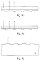
- Fig. 3 shows the inventive design of the individual parts of a contact within of an inverter.
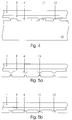
- Fig. 4 shows the mode of operation of the inventive design of the contacting within of an inverter.
- FIG. 6 shows various configurations of the inventive contacting in a top view.
- Fig. 1 shows an embodiment of a contact within a converter according to the State of the art.
- the counterpart (1) of the contact (21) has a conductive layer (3) with warts arranged thereon (4) which, when the converter is in pressure contact electrically conductive connection between the contact (21) and its counterpart (1) produce.
- the conductive surface is on the very small contact area (22) limited.
- Fig. 3 shows the inventive design of the individual parts of a contact within of an inverter.
- the contact (10) configured as a one-piece metal pressed part has Elevations (11) on (Fig. 3c).
- the counterpart (1) has, for example, an inside the same lying electrically conductive layer with connections to that of the contact (10) facing surface. These connections are electrically conductive with them connected warts made of soft solder arranged (Fig. 3a).
- Another embodiment (Fig. 3b) of the counterpart (1) of the contact (10) already corresponds to that in Fig. 1 described with an electrically conductive layer (3) on the contact facing side and warts arranged thereon (4).
- the contact (10) is arranged in relation to its counterpart (1) that the elevations (11) of the contact (10) are not the base of the warts (4) cover completely, but have a lateral offset.
- the warts are pressurized by the pressure-contacted structure of the converter the elevations are partially deformed such that there is a contact surface (12) between the Elevations (11) and the warts (4), which in their entirety results in at least one fifth the base of the warts.
- FIG. 5 shows a further embodiment of the contacting according to the invention.
- the Base area of the elevations (11) is smaller than the base area of the warts (4) (Fig. 5a). Also this results in a pressure after the pressure-contacted structure (FIG. 5b) is initiated Deformation of the warts (4) such that the respective contact area (12) is larger than one Fifth of the wart base area.
- FIG. 6 shows various configurations of the inventive contacting in a top view.
- FIG. 6a shows the top view of the embodiment according to FIG. 4.
- the portion is parallel to Surface of the counterpart (1) of the contact (10), the contact area between the Elevations (11) and the warts (4) and their arrangement in series can be clearly seen.
- Fig. 6b shows an embodiment with an offset of the warts (4) to the contact (10) not in the direction of the longitudinal extent of the contact, but orthogonally to it.
- 6c shows a further inventive embodiment in such a way that not only one survey a wart (4) but two warts are assigned. Furthermore, the warts (4) and elevations (11) assigned to them are arranged in a matrix. 6d shows that each a wart (4) two surveys (11) are assigned.
Landscapes
- Inverter Devices (AREA)
- Secondary Cells (AREA)
- Switches Operated By Changes In Physical Conditions (AREA)
- Die Bonding (AREA)
- Contacts (AREA)
- Coupling Device And Connection With Printed Circuit (AREA)
- Wire Bonding (AREA)
Abstract
eine Kontaktierung (10) eines Stromanschlusselements mit dem Substrat oder dem Gleichstromzwischenkreis Erhebungen (11) aufweist sowie deren Gegenstück (1) an den Kontaktstellen verformbare Warzen (4), wobei die Grundflächen der Warzen (4) durch die Erhebungen (11) nur teilweise überdeckt werden und die Warzen mittels der Druckkontaktierung durch die Erhebungen derart verformt werden, dass die gemeinsame Kontaktfläche (12) einer Warze (4) und einer Erhebung (11) mindestens ein Fünftel der Grundfläche einer Warze (4) aufweist.
Description
Claims (8)
- Umrichter in Druckkontaktierung bestehend aus einem Grundkörper, einem Substrat mit darauf angeordneten schaltungsgerecht miteinander verbundenen Halbleiterbauelementen sowie auf diesem Substrat vorgesehenen Kontaktflächen, Stromanschlusselementen für Gleich- und Wechselspannungsanschlüsse zur Kontaktierung dieser Kontaktflächen sowie zur Kontaktierung einer Gleichstromzwischenkreisplatine sowie des Wechselstromanschlusses, wobei mindestens eine Kontaktierung (10) mindestens eines Stromanschlusselements mit dem Substrat und / oder dem Gleichstromzwischenkreis und / oder dem Wechselstromanschluss Erhebungen (11) aufweist, und wobei das Gegenstück (1) an den Kontaktstellen verformbare Warzen (4) aufweist, wobei die Grundflächen der Warzen (4) durch die Erhebungen (11) nur teilweise überdeckt werden und die Warzen mittels der Druckkontaktierung durch die Erhebungen derart verformt werden, dass die gemeinsame Kontaktfläche (12) einer Warze (4) und einer Erhebung (11) mindestens ein Fünftel der Grundfläche einer Warze (4) aufweist.
- Schaltungsanordnung nach Anspruch 1, dadurch gekennzeichnet, dass jeder Erhebung (11) genau eine Warze (4) zugeordnet ist.
- Schaltungsanordnung nach Anspruch 1, dadurch gekennzeichnet, dass jeder Erhebung (11) mindestens zwei Warzen (4) zugeordnet sind.
- Schaltungsanordnung nach Anspruch 1, dadurch gekennzeichnet, dass einer Warze (4) mehr als jeder Erhebung (11) zugeordnet ist.
- Schaltungsanordnung nach Anspruch 1, dadurch gekennzeichnet, dass die Warzen (4) und die Erhebungen (11) in Reihe angeordnet sind.
- Schaltungsanordnung nach Anspruch 1, dadurch gekennzeichnet, dass die Warzen (4) und die zugeordneten Erhebungen (11) matrixartig angeordnet sind.
- Schaltungsanordnung nach Anspruch 1, dadurch gekennzeichnet, dass die Warzen (4) aus einem handelsüblichen Weichlot bestehen.
- Schaltungsanordnung nach Anspruch 1, dadurch gekennzeichnet, dass die Anschlusselemente (10) mit den Erhebungen (11) einstückige Metallpressteile sind.
Applications Claiming Priority (2)
| Application Number | Priority Date | Filing Date | Title |
|---|---|---|---|
| DE10159119 | 2001-12-01 | ||
| DE10159119A DE10159119B4 (de) | 2001-12-01 | 2001-12-01 | Umrichter in Druckkontaktierung |
Publications (3)
| Publication Number | Publication Date |
|---|---|
| EP1316997A2 true EP1316997A2 (de) | 2003-06-04 |
| EP1316997A3 EP1316997A3 (de) | 2006-02-08 |
| EP1316997B1 EP1316997B1 (de) | 2007-10-17 |
Family
ID=7707751
Family Applications (1)
| Application Number | Title | Priority Date | Filing Date |
|---|---|---|---|
| EP02026281A Expired - Lifetime EP1316997B1 (de) | 2001-12-01 | 2002-11-27 | Umrichter in Druckkontaktierung |
Country Status (5)
| Country | Link |
|---|---|
| EP (1) | EP1316997B1 (de) |
| AT (1) | ATE376253T1 (de) |
| DE (2) | DE10159119B4 (de) |
| DK (1) | DK1316997T3 (de) |
| ES (1) | ES2292677T3 (de) |
Family Cites Families (5)
| Publication number | Priority date | Publication date | Assignee | Title |
|---|---|---|---|---|
| US5329423A (en) * | 1993-04-13 | 1994-07-12 | Scholz Kenneth D | Compressive bump-and-socket interconnection scheme for integrated circuits |
| US5499924A (en) * | 1993-07-12 | 1996-03-19 | Kel Comporation | Butt joint connector assembly |
| GB9400384D0 (en) * | 1994-01-11 | 1994-03-09 | Inmos Ltd | Circuit connection in an electrical assembly |
| DE19942770A1 (de) * | 1999-09-08 | 2001-03-15 | Ixys Semiconductor Gmbh | Leistungshalbleiter-Modul |
| DE10127947C1 (de) * | 2001-08-22 | 2002-10-17 | Semikron Elektronik Gmbh | Schaltungsanordnung |
-
2001
- 2001-12-01 DE DE10159119A patent/DE10159119B4/de not_active Expired - Lifetime
-
2002
- 2002-11-27 AT AT02026281T patent/ATE376253T1/de active
- 2002-11-27 DK DK02026281T patent/DK1316997T3/da active
- 2002-11-27 EP EP02026281A patent/EP1316997B1/de not_active Expired - Lifetime
- 2002-11-27 DE DE50211078T patent/DE50211078D1/de not_active Expired - Lifetime
- 2002-11-27 ES ES02026281T patent/ES2292677T3/es not_active Expired - Lifetime
Also Published As
| Publication number | Publication date |
|---|---|
| ATE376253T1 (de) | 2007-11-15 |
| DE50211078D1 (de) | 2007-11-29 |
| EP1316997B1 (de) | 2007-10-17 |
| DE10159119A1 (de) | 2003-06-18 |
| DE10159119B4 (de) | 2005-02-17 |
| EP1316997A3 (de) | 2006-02-08 |
| ES2292677T3 (es) | 2008-03-16 |
| DK1316997T3 (da) | 2008-02-25 |
Similar Documents
| Publication | Publication Date | Title |
|---|---|---|
| DE69602202T2 (de) | Elektrischer kontakt mit verringerter selbstinduktivität | |
| EP1713124B1 (de) | Leistungshalbleitermodul mit Verbindungsbahnen und mit Anschlusselementen, die mit den Verbindungsbahnen verbunden sind | |
| DE69129619T2 (de) | Halbleitervorrichtung mit einer vielzahl von anschlussstiften | |
| EP1898466B1 (de) | Gehauste Halbleiterschaltungsanordnung mit Kontakteinrichtung | |
| DE69417988T2 (de) | Leiterplattenrandverbinder mit Kontakten von verminderten Teilung | |
| DE10306643A1 (de) | Druckkontaktierung für ein Leistungshalbleitermodul | |
| DE10333329B4 (de) | Leistungshalbleitermodul mit biegesteifer Grundplatte | |
| DE102020111526B3 (de) | Leistungshalbleitermodul mit Einpresskontaktelement | |
| DE19522172C1 (de) | Leistungs-Halbleitermodul mit Anschlußstiften | |
| DE102019117476B4 (de) | Leistungselektronische Schalteinrichtung mit einem Anschlusselement | |
| DE69525302T2 (de) | Oberflächenmontierter Verbinder | |
| DE10017746B4 (de) | Verfahren zur Herstellung eines elektronischen Bauteils mit mikroskopisch kleinen Kontaktflächen | |
| EP1940207A2 (de) | Elektrische Vorrichtung mit einem Trägerelement mit zumindest einer speziellen Anschlussfläche und einem oberflächenmontierten Bauelement | |
| DE102006058694B4 (de) | Leistungshalbleitermodul mit Kontaktfedern | |
| EP1220314A2 (de) | Leistungshalbleitermodul | |
| DE102017211336B4 (de) | Leistungsmodul mit oberflächenmontierten elektrischen Kontaktierungselementen | |
| DE102012218433B4 (de) | Kontaktanordnung | |
| DE1514562B2 (de) | Anordnung zur herstellung eines halbleiter-bauelementes | |
| DE10159119B4 (de) | Umrichter in Druckkontaktierung | |
| EP0238823B1 (de) | Steckverbinderleiste mit in mindestens zwei parallelen Reihen angeordneten Kontaktfedern | |
| DE102006058695B4 (de) | Leistungshalbleitermodul mit stumpf gelötetem Anschlusselement | |
| DE102016209604A1 (de) | Einpress-Anschluss, Halbleitervorrichtung, Leistungswandlungsvorrichtung und Verfahren zur Herstellung eines Einpress-Anschlusses | |
| DE10047153B4 (de) | Befestigungseinrichtung | |
| EP2003693A2 (de) | Druckkontaktiertes dreiphasiges Stromrichtermodul | |
| DE102006062313A1 (de) | Elektrische Steckerleiste |
Legal Events
| Date | Code | Title | Description |
|---|---|---|---|
| PUAI | Public reference made under article 153(3) epc to a published international application that has entered the european phase |
Free format text: ORIGINAL CODE: 0009012 |
|
| AK | Designated contracting states |
Designated state(s): AT BE BG CH CY CZ DE DK EE ES FI FR GB GR IE IT LI LU MC NL PT SE SK TR |
|
| AX | Request for extension of the european patent |
Extension state: AL LT LV MK RO SI |
|
| RAP1 | Party data changed (applicant data changed or rights of an application transferred) |
Owner name: SEMIKRON ELEKTRONIK GMBH & CO. KG |
|
| PUAL | Search report despatched |
Free format text: ORIGINAL CODE: 0009013 |
|
| AK | Designated contracting states |
Kind code of ref document: A3 Designated state(s): AT BE BG CH CY CZ DE DK EE ES FI FR GB GR IE IT LI LU MC NL PT SE SK TR |
|
| AX | Request for extension of the european patent |
Extension state: AL LT LV MK RO SI |
|
| 17P | Request for examination filed |
Effective date: 20060106 |
|
| AKX | Designation fees paid |
Designated state(s): AT BE BG CH CY CZ DE DK EE ES FI FR GB GR IE IT LI LU MC NL PT SE SK TR |
|
| 17Q | First examination report despatched |
Effective date: 20060412 |
|
| GRAP | Despatch of communication of intention to grant a patent |
Free format text: ORIGINAL CODE: EPIDOSNIGR1 |
|
| GRAS | Grant fee paid |
Free format text: ORIGINAL CODE: EPIDOSNIGR3 |
|
| GRAA | (expected) grant |
Free format text: ORIGINAL CODE: 0009210 |
|
| AK | Designated contracting states |
Kind code of ref document: B1 Designated state(s): AT BE BG CH CY CZ DE DK EE ES FI FR GB GR IE IT LI LU MC NL PT SE SK TR |
|
| REG | Reference to a national code |
Ref country code: GB Ref legal event code: FG4D Free format text: NOT ENGLISH |
|
| REG | Reference to a national code |
Ref country code: CH Ref legal event code: EP |
|
| REG | Reference to a national code |
Ref country code: IE Ref legal event code: FG4D Free format text: LANGUAGE OF EP DOCUMENT: GERMAN |
|
| REF | Corresponds to: |
Ref document number: 50211078 Country of ref document: DE Date of ref document: 20071129 Kind code of ref document: P |
|
| REG | Reference to a national code |
Ref country code: CH Ref legal event code: NV Representative=s name: BRAUNPAT BRAUN EDER AG |
|
| GBT | Gb: translation of ep patent filed (gb section 77(6)(a)/1977) |
Effective date: 20071212 |
|
| REG | Reference to a national code |
Ref country code: SE Ref legal event code: TRGR |
|
| REG | Reference to a national code |
Ref country code: DK Ref legal event code: T3 |
|
| REG | Reference to a national code |
Ref country code: ES Ref legal event code: FG2A Ref document number: 2292677 Country of ref document: ES Kind code of ref document: T3 |
|
| ET | Fr: translation filed | ||
| PG25 | Lapsed in a contracting state [announced via postgrant information from national office to epo] |
Ref country code: BG Free format text: LAPSE BECAUSE OF FAILURE TO SUBMIT A TRANSLATION OF THE DESCRIPTION OR TO PAY THE FEE WITHIN THE PRESCRIBED TIME-LIMIT Effective date: 20080117 Ref country code: PT Free format text: LAPSE BECAUSE OF FAILURE TO SUBMIT A TRANSLATION OF THE DESCRIPTION OR TO PAY THE FEE WITHIN THE PRESCRIBED TIME-LIMIT Effective date: 20080317 |
|
| REG | Reference to a national code |
Ref country code: IE Ref legal event code: FD4D |
|
| PG25 | Lapsed in a contracting state [announced via postgrant information from national office to epo] |
Ref country code: MC Free format text: LAPSE BECAUSE OF NON-PAYMENT OF DUE FEES Effective date: 20071130 |
|
| PG25 | Lapsed in a contracting state [announced via postgrant information from national office to epo] |
Ref country code: CZ Free format text: LAPSE BECAUSE OF FAILURE TO SUBMIT A TRANSLATION OF THE DESCRIPTION OR TO PAY THE FEE WITHIN THE PRESCRIBED TIME-LIMIT Effective date: 20071017 |
|
| PLBE | No opposition filed within time limit |
Free format text: ORIGINAL CODE: 0009261 |
|
| STAA | Information on the status of an ep patent application or granted ep patent |
Free format text: STATUS: NO OPPOSITION FILED WITHIN TIME LIMIT |
|
| PG25 | Lapsed in a contracting state [announced via postgrant information from national office to epo] |
Ref country code: SK Free format text: LAPSE BECAUSE OF FAILURE TO SUBMIT A TRANSLATION OF THE DESCRIPTION OR TO PAY THE FEE WITHIN THE PRESCRIBED TIME-LIMIT Effective date: 20071017 |
|
| 26N | No opposition filed |
Effective date: 20080718 |
|
| PG25 | Lapsed in a contracting state [announced via postgrant information from national office to epo] |
Ref country code: IE Free format text: LAPSE BECAUSE OF FAILURE TO SUBMIT A TRANSLATION OF THE DESCRIPTION OR TO PAY THE FEE WITHIN THE PRESCRIBED TIME-LIMIT Effective date: 20071017 |
|
| PG25 | Lapsed in a contracting state [announced via postgrant information from national office to epo] |
Ref country code: EE Free format text: LAPSE BECAUSE OF FAILURE TO SUBMIT A TRANSLATION OF THE DESCRIPTION OR TO PAY THE FEE WITHIN THE PRESCRIBED TIME-LIMIT Effective date: 20071017 Ref country code: GR Free format text: LAPSE BECAUSE OF FAILURE TO SUBMIT A TRANSLATION OF THE DESCRIPTION OR TO PAY THE FEE WITHIN THE PRESCRIBED TIME-LIMIT Effective date: 20080118 |
|
| PG25 | Lapsed in a contracting state [announced via postgrant information from national office to epo] |
Ref country code: FI Free format text: LAPSE BECAUSE OF FAILURE TO SUBMIT A TRANSLATION OF THE DESCRIPTION OR TO PAY THE FEE WITHIN THE PRESCRIBED TIME-LIMIT Effective date: 20071017 |
|
| PG25 | Lapsed in a contracting state [announced via postgrant information from national office to epo] |
Ref country code: CY Free format text: LAPSE BECAUSE OF FAILURE TO SUBMIT A TRANSLATION OF THE DESCRIPTION OR TO PAY THE FEE WITHIN THE PRESCRIBED TIME-LIMIT Effective date: 20071017 |
|
| PG25 | Lapsed in a contracting state [announced via postgrant information from national office to epo] |
Ref country code: LU Free format text: LAPSE BECAUSE OF NON-PAYMENT OF DUE FEES Effective date: 20071127 |
|
| PG25 | Lapsed in a contracting state [announced via postgrant information from national office to epo] |
Ref country code: TR Free format text: LAPSE BECAUSE OF FAILURE TO SUBMIT A TRANSLATION OF THE DESCRIPTION OR TO PAY THE FEE WITHIN THE PRESCRIBED TIME-LIMIT Effective date: 20071017 |
|
| REG | Reference to a national code |
Ref country code: FR Ref legal event code: PLFP Year of fee payment: 14 |
|
| REG | Reference to a national code |
Ref country code: FR Ref legal event code: PLFP Year of fee payment: 15 |
|
| PGFP | Annual fee paid to national office [announced via postgrant information from national office to epo] |
Ref country code: DK Payment date: 20161124 Year of fee payment: 15 Ref country code: NL Payment date: 20161124 Year of fee payment: 15 |
|
| PGFP | Annual fee paid to national office [announced via postgrant information from national office to epo] |
Ref country code: SE Payment date: 20161124 Year of fee payment: 15 Ref country code: BE Payment date: 20161124 Year of fee payment: 15 Ref country code: AT Payment date: 20161122 Year of fee payment: 15 |
|
| REG | Reference to a national code |
Ref country code: FR Ref legal event code: PLFP Year of fee payment: 16 |
|
| REG | Reference to a national code |
Ref country code: CH Ref legal event code: PCAR Free format text: NEW ADDRESS: HOLEESTRASSE 87, 4054 BASEL (CH) |
|
| REG | Reference to a national code |
Ref country code: DK Ref legal event code: EBP Effective date: 20171130 |
|
| REG | Reference to a national code |
Ref country code: SE Ref legal event code: EUG |
|
| REG | Reference to a national code |
Ref country code: NL Ref legal event code: MM Effective date: 20171201 |
|
| REG | Reference to a national code |
Ref country code: AT Ref legal event code: MM01 Ref document number: 376253 Country of ref document: AT Kind code of ref document: T Effective date: 20171127 |
|
| PG25 | Lapsed in a contracting state [announced via postgrant information from national office to epo] |
Ref country code: SE Free format text: LAPSE BECAUSE OF NON-PAYMENT OF DUE FEES Effective date: 20171128 Ref country code: AT Free format text: LAPSE BECAUSE OF NON-PAYMENT OF DUE FEES Effective date: 20171127 |
|
| REG | Reference to a national code |
Ref country code: BE Ref legal event code: MM Effective date: 20171130 |
|
| PG25 | Lapsed in a contracting state [announced via postgrant information from national office to epo] |
Ref country code: NL Free format text: LAPSE BECAUSE OF NON-PAYMENT OF DUE FEES Effective date: 20171201 |
|
| PG25 | Lapsed in a contracting state [announced via postgrant information from national office to epo] |
Ref country code: DK Free format text: LAPSE BECAUSE OF NON-PAYMENT OF DUE FEES Effective date: 20171130 Ref country code: BE Free format text: LAPSE BECAUSE OF NON-PAYMENT OF DUE FEES Effective date: 20171130 |
|
| PGFP | Annual fee paid to national office [announced via postgrant information from national office to epo] |
Ref country code: DE Payment date: 20211130 Year of fee payment: 20 Ref country code: GB Payment date: 20211123 Year of fee payment: 20 Ref country code: ES Payment date: 20211216 Year of fee payment: 20 Ref country code: FR Payment date: 20211119 Year of fee payment: 20 |
|
| PGFP | Annual fee paid to national office [announced via postgrant information from national office to epo] |
Ref country code: IT Payment date: 20211130 Year of fee payment: 20 Ref country code: CH Payment date: 20211123 Year of fee payment: 20 |
|
| REG | Reference to a national code |
Ref country code: DE Ref legal event code: R071 Ref document number: 50211078 Country of ref document: DE |
|
| REG | Reference to a national code |
Ref country code: CH Ref legal event code: PL |
|
| REG | Reference to a national code |
Ref country code: GB Ref legal event code: PE20 Expiry date: 20221126 |
|
| PG25 | Lapsed in a contracting state [announced via postgrant information from national office to epo] |
Ref country code: GB Free format text: LAPSE BECAUSE OF EXPIRATION OF PROTECTION Effective date: 20221126 |
|
| REG | Reference to a national code |
Ref country code: ES Ref legal event code: FD2A Effective date: 20230427 |
|
| PG25 | Lapsed in a contracting state [announced via postgrant information from national office to epo] |
Ref country code: ES Free format text: LAPSE BECAUSE OF EXPIRATION OF PROTECTION Effective date: 20221128 |