EP1316995A1 - Semiconductor device and method for manufacturing the same - Google Patents
Semiconductor device and method for manufacturing the same Download PDFInfo
- Publication number
- EP1316995A1 EP1316995A1 EP01956884A EP01956884A EP1316995A1 EP 1316995 A1 EP1316995 A1 EP 1316995A1 EP 01956884 A EP01956884 A EP 01956884A EP 01956884 A EP01956884 A EP 01956884A EP 1316995 A1 EP1316995 A1 EP 1316995A1
- Authority
- EP
- European Patent Office
- Prior art keywords
- interconnect
- interconnects
- insulating layer
- interlayer insulating
- semiconductor device
- Prior art date
- Legal status (The legal status is an assumption and is not a legal conclusion. Google has not performed a legal analysis and makes no representation as to the accuracy of the status listed.)
- Granted
Links
Images




Classifications
-
- H—ELECTRICITY
- H10—SEMICONDUCTOR DEVICES; ELECTRIC SOLID-STATE DEVICES NOT OTHERWISE PROVIDED FOR
- H10W—GENERIC PACKAGES, INTERCONNECTIONS, CONNECTORS OR OTHER CONSTRUCTIONAL DETAILS OF DEVICES COVERED BY CLASS H10
- H10W20/00—Interconnections in chips, wafers or substrates
- H10W20/01—Manufacture or treatment
-
- H—ELECTRICITY
- H10—SEMICONDUCTOR DEVICES; ELECTRIC SOLID-STATE DEVICES NOT OTHERWISE PROVIDED FOR
- H10W—GENERIC PACKAGES, INTERCONNECTIONS, CONNECTORS OR OTHER CONSTRUCTIONAL DETAILS OF DEVICES COVERED BY CLASS H10
- H10W20/00—Interconnections in chips, wafers or substrates
- H10W20/40—Interconnections external to wafers or substrates, e.g. back-end-of-line [BEOL] metallisations or vias connecting to gate electrodes
- H10W20/495—Capacitive arrangements or effects of, or between wiring layers
-
- H—ELECTRICITY
- H10—SEMICONDUCTOR DEVICES; ELECTRIC SOLID-STATE DEVICES NOT OTHERWISE PROVIDED FOR
- H10W—GENERIC PACKAGES, INTERCONNECTIONS, CONNECTORS OR OTHER CONSTRUCTIONAL DETAILS OF DEVICES COVERED BY CLASS H10
- H10W20/00—Interconnections in chips, wafers or substrates
- H10W20/01—Manufacture or treatment
- H10W20/071—Manufacture or treatment of dielectric parts thereof
- H10W20/072—Manufacture or treatment of dielectric parts thereof of dielectric parts comprising air gaps
-
- H—ELECTRICITY
- H10—SEMICONDUCTOR DEVICES; ELECTRIC SOLID-STATE DEVICES NOT OTHERWISE PROVIDED FOR
- H10W—GENERIC PACKAGES, INTERCONNECTIONS, CONNECTORS OR OTHER CONSTRUCTIONAL DETAILS OF DEVICES COVERED BY CLASS H10
- H10W20/00—Interconnections in chips, wafers or substrates
- H10W20/01—Manufacture or treatment
- H10W20/071—Manufacture or treatment of dielectric parts thereof
- H10W20/074—Manufacture or treatment of dielectric parts thereof of dielectric parts comprising thin functional dielectric layers, e.g. dielectric etch-stop, barrier, capping or liner layers
-
- H—ELECTRICITY
- H10—SEMICONDUCTOR DEVICES; ELECTRIC SOLID-STATE DEVICES NOT OTHERWISE PROVIDED FOR
- H10W—GENERIC PACKAGES, INTERCONNECTIONS, CONNECTORS OR OTHER CONSTRUCTIONAL DETAILS OF DEVICES COVERED BY CLASS H10
- H10W20/00—Interconnections in chips, wafers or substrates
- H10W20/01—Manufacture or treatment
- H10W20/071—Manufacture or treatment of dielectric parts thereof
- H10W20/074—Manufacture or treatment of dielectric parts thereof of dielectric parts comprising thin functional dielectric layers, e.g. dielectric etch-stop, barrier, capping or liner layers
- H10W20/077—Manufacture or treatment of dielectric parts thereof of dielectric parts comprising thin functional dielectric layers, e.g. dielectric etch-stop, barrier, capping or liner layers on sidewalls or on top surfaces of conductors
-
- H—ELECTRICITY
- H10—SEMICONDUCTOR DEVICES; ELECTRIC SOLID-STATE DEVICES NOT OTHERWISE PROVIDED FOR
- H10W—GENERIC PACKAGES, INTERCONNECTIONS, CONNECTORS OR OTHER CONSTRUCTIONAL DETAILS OF DEVICES COVERED BY CLASS H10
- H10W20/00—Interconnections in chips, wafers or substrates
- H10W20/01—Manufacture or treatment
- H10W20/071—Manufacture or treatment of dielectric parts thereof
- H10W20/098—Manufacture or treatment of dielectric parts thereof by filling between adjacent conductive parts
-
- H—ELECTRICITY
- H10—SEMICONDUCTOR DEVICES; ELECTRIC SOLID-STATE DEVICES NOT OTHERWISE PROVIDED FOR
- H10W—GENERIC PACKAGES, INTERCONNECTIONS, CONNECTORS OR OTHER CONSTRUCTIONAL DETAILS OF DEVICES COVERED BY CLASS H10
- H10W20/00—Interconnections in chips, wafers or substrates
- H10W20/40—Interconnections external to wafers or substrates, e.g. back-end-of-line [BEOL] metallisations or vias connecting to gate electrodes
- H10W20/45—Interconnections external to wafers or substrates, e.g. back-end-of-line [BEOL] metallisations or vias connecting to gate electrodes characterised by their insulating parts
- H10W20/46—Interconnections external to wafers or substrates, e.g. back-end-of-line [BEOL] metallisations or vias connecting to gate electrodes characterised by their insulating parts comprising air gaps
Definitions
- the present invention relates to semiconductor devices and methods of producing the same.
- a semiconductor device is formed by providing a plurality of interconnects and a plurality of electronic components on a substrate using a wafer.
- the interconnects are formed to project on the substrate by dry etching for instance, the surface of the substrate on which surface the interconnects are not formed is further covered, and at the same time, the spaces between the interconnects are filled with an interlayer insulating layer. Further, in this case, when the interlayer insulating layer is formed in multiple layers, the process of forming the interconnects and the process of forming the interlayer insulating layer are repeated a desired number of times. Alternately, the interconnects are also buried and formed in the substrate by a damascene process.
- interconnect delay becomes an issue.
- the interconnect delay is proportional to the electric resistance of metal employed in the interconnects and the parasitic capacitance between the interconnect and the substrate or between the interconnects.
- a material having a small dielectric constant is selected as the interlayer insulating layer, or it is considered to increase the interconnect pitch, at the stage of circuit designing, at a point where the interconnect delay becomes a problem.
- the former method of selecting a material of a small dielectric constant as the interlayer insulating layer can do no more than reduce the dielectric constant to at most two, and therefore, does not necessarily achieve the effect of reducing the interconnect delay sufficiently.
- the progressing miniaturization leaves only a little room for the method of increasing the interconnect pitch to be employed.
- the interconnect pitch may be unchangeable due to layout restrictions on the disposition of electronic components.
- this method does not necessarily achieve the effect of reducing the interconnect delay sufficiently, either.
- the latter air isolation method which still has a lot of problems including the securing of interconnect reliability, that is, the prevention of the deformation or breaking of the formed interconnects, has yet to be put to practical use.
- the present invention is made in view of the above-described problems, and has an object of providing a semiconductor device having reduced interconnect delay and increased reliability and a method of manufacturing the same.
- a semiconductor device which is formed by forming insulating layers on a substrate on which at least two or more interconnects are formed so as to project therefrom, is characterized in that an insulating film is buried selectively in a space between adjacent interconnects in which space interconnect delay is predicted to fall below a predetermined value due to interconnect design.
- interconnect delay is proportional to each of the electric resistance of an interconnect and the parasitic capacitance between interconnects.
- the former electric resistance and the latter capacitance are inversely proportional to the interconnect width and the interconnect pitch, respectively. Therefore, the magnitude of the interconnect delay can be predicted with respect to each interconnect. Accordingly, in the interconnect design, the space between interconnects where the interconnect delay exceeds a predetermined value and the space between interconnects where the interconnect delay falls below the predetermined value can be specified.
- the air isolation method which forms a gap between interconnects, can reduce the interconnect delay.
- no insulating film is buried in the spaces between interconnects, so that the formed interconnects may be deformed or broken.
- an insulating film is buried selectively in the space between adjacent interconnects where the interconnect delay is predicted to fall below a predetermined value due to the interconnect design. Therefore, the interconnect delay is reduced, so that a semiconductor device having high interconnect reliability can be obtained.
- both upper and lower insulating layers may be formed of hydrophilic material, and a special layer formed of hydrophobic material may be provided between the upper and lower interlayer insulating layers.
- the semiconductor device is suitably formed by alternately forming the interconnects and the insulating layer so that two or more layers of the interconnects and two or more layers of the insulating layer are formed.
- the interconnects of the second layer are formed on the first insulating layer (interlayer insulating layer) so as to project therefrom, and the second insulating layer (interlayer insulating layer) is formed on the first insulating layer and the interconnects of the second layer.
- a method of manufacturing a semiconductor device which method includes an interconnect forming step of forming at least two or more interconnects on a substrate so that the interconnects project therefrom and an interlayer insulating layer forming step of forming an interlayer insulating layer, is characterized by including an adhesion inhibiting layer forming step of forming an adhesion inhibiting layer inhibiting adhesion to the interlayer insulating layer between the interconnect forming step and the interlayer insulating layer forming step.
- interconnect forming step at least two or more interconnects may be suitably formed on the substrate so that the interconnects project therefrom by, for instance, a method forming an interconnect layer and thereafter performing dry etching using a predetermined mask.
- this is not the only method.
- the interlayer insulating layer may be suitably formed by a method applying inorganic or organic insulating material paste. However, this is not the only method.
- the adhesion inhibiting layer inhibiting adhesion may be suitably formed by a method forming one of the interlayer insulating layer and the adhesion inhibiting layer of hydrophilic material and the other of hydrophobic material in light of reducing wettability. For instance, a method that applies by printing or attaches by surface processing an adhesion inhibiting material only to the region between adjacent interconnects in which region the interconnect delay is predicted to exceed a predetermined value due to the interconnect design is employable. However, this is not the only method.
- the adhesion inhibiting layer can be suitably formed with a reduced number of steps, so that a semiconductor device having a small interconnect delay can be obtained.
- the adhesion inhibiting layer is more preferably formed in the space between adjacent interconnects in which space the interconnect delay is predicted to exceed the predetermined value.
- the interconnect forming step and the interlayer insulating layer forming step may be repeated two or more times, and an insulating paste viscosity control step of controlling viscosity of insulating paste that is a material forming the interlayer insulating layer so as to prevent the insulating paste from entering only the space between adjacent interconnects may be performed at least once as a replacement instead of the adhesion inhibiting layer forming step.
- the effects of the present invention may also be produced, without providing the adhesion inhibiting layer forming step, by the interlayer insulating layer forming step including the insulating paste viscosity control step of controlling viscosity of insulating paste that is a material forming the interlayer insulating layer so as to prevent the insulating paste from entering only the space between adjacent interconnects.
- the adjacent interconnects where the interconnect delay is predicted to exceed the predetermined value have a small interconnect pitch when the interconnects are formed to have a uniform width. Accordingly, by controlling the viscosity of the insulating paste to a value large enough to prevent the insulating paste from entering and filling the space of the small interconnect pitch, a gap can be left in the space between the adjacent interconnects.
- the predetermined viscosity of the insulating paste can be suitably set by collecting data by repeating the test of applying and forming insulating pastes of different viscosities on a substrate with different interconnect pitches.
- a transistor semiconductor device
- a substrate formed of a wafer a transistor forming process S1, the substrate and the transistor not shown in the drawings.
- an interconnect layer is formed on the base insulating layer 10.
- a plurality of interconnects (interconnect patterns) 12a through 12f are formed by dry etching with different interconnect pitches P1 through P3 (an interconnect forming process S3, FIG. 3).
- Al is employed as the interconnect material.
- necessary contact holes are formed in the base insulating layer 10, and contacts are further formed (not shown in the drawing).
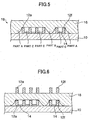
- an adhesion inhibiting layer for inhibiting adhesion to a later-described interlayer insulating layer is formed only in the space between adjacent interconnects where the interconnect delay is predicted to exceed a predetermined value due to the interconnect design (an adhesion inhibiting layer forming process S4, FIG. 4).
- the interconnect delay is predicted to exceed the predetermined value in the spaces between the interconnects 12a and 12b, 12b and 12c, 12c and 12d, and 12e and 12f having the smaller interconnect pitches (P1 in FIG. 3).
- the interconnect delay is predicted to fall below the predetermined value in the spaces between the interconnects 12d and 12e, the interconnect 12a and its adjacent interconnect not shown in the drawing, and the interconnect 12f and its adjacent interconnect not shown in the drawing having the larger interconnect pitches (P2 and P3 in FIG. 3).
- the spaces between the interconnects 12a and 12b, 12b and 12c, 12c and 12d, and 12e and 12f having the smaller interconnect pitches are coated with an adhesion inhibiting agent, so that an adhesion inhibiting layer 14 is formed.
- HMDS hexamethyldisilazane
- FIG. 5 provides a pictorial or schematic representation for convenience of description.
- interconnect forming process adhesion inhibiting layer forming process, and interlayer insulating layer forming process may be further repeated one or a plurality of times as required so that a semiconductor device having multiple interconnect layers and interlayer insulating layers formed therein is formed.
- step 6 the interconnect forming process (FIG. 6), the adhesion inhibiting layer forming process (FIG. 7), and the interlayer insulating layer forming process (FIG. 8) that are steps 3 (S3) through 5 (S5), and processes including baking are performed (a multilayer forming process S7, FIGS. 6 through 8).
- a semiconductor device 20 having multiple interconnect layers and interlayer insulating layers formed therein is completed (step 8, FIG. 8).
- a gap is formed between the adjacent interconnects having a small interconnect pitch. Therefore, the dielectric constant between the interconnects decreases so as to reduce the interconnect delay. Further, since an insulating film is buried selectively in a space between adjacent interconnects of a large interconnect pitch, the interconnect reliability can be secured.
- the adhesion inhibiting layer is provided for intervention for each of the interlayer insulating layers for the purpose of inhibiting adhesion.
- a later-described method of controlling the viscosity of insulating paste in forming the interlayer insulating layers may be employed.
- the method of manufacturing a semiconductor device is basically the same. Therefore, the same elements as those of the first embodiment are referred to by the same numerals as those of the first embodiment, and a graphical representation of each manufacturing process will be omitted. Further, a description of the processes of manufacturing second and subsequent interlayer insulating layers will be omitted.
- the base insulating layer 10 including TEOS is formed on it (a base insulating layer forming process). Further, the interconnects 12a through 12f are formed using Al material on the base insulating layer 10 by dry etching with the different interconnect pitches P1 through P3 (see FIG. 3) (an interconnect forming process), and contacts are formed.
- SiLK (a registered trademark of The Dow Chemical Company), which is a hydrophobic organic material, for instance, is applied as insulating paste so that the interlayer insulating layer 16 is formed (an interlayer insulating layer forming process).
- SiLK is applied on the base insulating layer 10. The viscosity is controlled by changing the proportion of a solvent for SiLK.
- the interlayer insulating layer 16 is caused to adhere to the base insulating layer 10 in the parts (parts A and B in FIG. 9) having no interconnect formed therein between the interconnects 12d and 12e, the interconnect 12a and its adjacent interconnect not shown in the drawing, and the interconnect 12f and its adjacent interconnect not shown in the drawing provided with the larger interconnect pitches (P2 and P3). Meanwhile, the interlayer insulating layer 16 is prevented from adhering to the base insulating layer 10 in the parts (parts C in FIG. 9) between the interconnects 12a and 12b, 12b and 12c, 12c and 12d, and 12e and 12f where the viscosity is high so as to make it difficult for SiLK to enter. Accordingly, gaps are formed in the parts C.
- a gap is formed between the adjacent interconnects having a small interconnect pitch. Therefore, the dielectric constant between the interconnects decreases so as to reduce the interconnect delay. Further, since an insulating film is buried selectively in a space between adjacent interconnects of a large interconnect pitch, the interconnect reliability can be secured.
- each layer is formed as in the semiconductor device 22 of the above-described second embodiment. That is, after forming the interconnects 12a through 12f using Al on the base insulating layer 10 (an interconnect forming process), SiLK whose viscosity is controlled to a predetermined value is applied so that the interlayer insulating layer 16 is formed (an interlayer insulating layer forming process). Then, curing and other processes for stabilizing the interlayer insulating layer 16 are performed.
- the second interconnect and interlayer insulating layers are formed by a method somewhat different from that in the case of the first layers.
- an oxide film 32 of hydrophilic SiO 2 is formed by, for instance, CVD selectively in the spaces between the interconnects 30a and 30b, 30b and 30c, 30c and 30d, and 30e and 30f having the smaller interconnect pitches (P1).
- a second interlayer insulating layer 34 is formed by applying SiLK whose viscosity is controlled to the predetermined value (an interlayer insulating layer forming process).
- the hydrophilic oxide film 32 is formed in the spaces between the interconnects 30a and 30b, 30b and 30c, 30c and 30d, and 30e and 30f having the smaller interconnect pitches (P1). Therefore, in the parts C, the hydrophobic interlayer insulating layer 34 is prevented from adhering to the hydrophobic interlayer insulating layer 16 (parts C in FIG. 10), so that gaps are formed.
- the hydrophobic interlayer insulating layer 34 suitably adheres to the exposed hydrophobic interlayer insulating layer 16 in the spaces between the interconnects 30d and 30e, 30a and its adjacent interconnect not shown in the drawing, and 30f and its adjacent interconnect not shown in the drawing having the larger interconnect pitches (P2 and P3) (parts A and B in FIG. 10).
- FIG. 10 a semiconductor device 36 having multiple interconnect layers and interlayer insulating layers formed therein is completed (FIG. 10).
- a gap is formed between the adjacent interconnects having a small interconnect pitch. Therefore, the dielectric constant between the interconnects decreases so as to reduce the interconnect delay. Further, since an insulating film is buried selectively in a space between adjacent interconnects of a large interconnect pitch, the interconnect reliability can be secured.
- each layer is formed as in the semiconductor device 22 of the above-described second embodiment. That is, after the interconnects 12a through 12f are formed using Al on the base insulating layer 10 (an interconnect forming process), SiLK whose viscosity is controlled to a predetermined value is applied so that the interlayer insulating layer 16 is formed (an interlayer insulating layer forming process). Then, curing and other processes for stabilizing the interlayer insulating layer 16 are performed.
- the second interconnect and interlayer insulating layers are formed by a method different from that in the case of the first layers.
- an organic thin film 42 of polymer material is formed by, for instance, CVD selectively in the spaces between the interconnects 40a and 40b, 40b and 40c, 40c and 40d, and 40e and 40f having the smaller interconnect pitches (P1, see FIG. 3).
- the degree of the hydrophobic property of the first hydrophobic interlayer insulating layer 16 can be further increased by forming the organic thin film 42 thereon.
- the organic thin film 42 serves as a layer inhibiting adhesion (an adhesion inhibiting layer forming process).
- MSQ which is inorganic material
- MSQ is applied, so that a second interlayer insulating layer 44 is formed (an interlayer insulating layer forming process).
- the interlayer insulating layer 44 adheres to the interlayer insulating layer 16 in the former (parts A and B in FIG. 11), while in the latter, the interlayer insulating layer 44 is prevented from adhering to the interlayer insulating layer 16 (organic thin film 42) (parts C in FIG. 9) so that gaps are formed in the parts C.
- the effect of the viscosity control and the effect of the organic thin film 42 are combined with each other to be suitably produced.
- a semiconductor device 46 having a plurality of interconnect layers and interlayer insulating layers are formed therein is completed (FIG. 11).
- the hydrophobic interlayer insulating film 16 and the hydrophilic interlayer insulating film 44 are alternately layered.
- a gap is formed between the adjacent interconnects having a small interconnect pitch. Therefore, the dielectric constant between the interconnects decreases so as to reduce the interconnect delay. Further, since an insulating film is buried selectively in a space between adjacent interconnects of a large interconnect pitch, the interconnect reliability can be secured.
- the method of manufacturing a semiconductor device of the present invention is not limited to the above-described first through fourth embodiments.
- the adhesion inhibiting layer may be formed over the entire surface of the substrate.
Landscapes
- Internal Circuitry In Semiconductor Integrated Circuit Devices (AREA)
- Crystals, And After-Treatments Of Crystals (AREA)
- Bipolar Transistors (AREA)
Abstract
Description
Claims (9)
- A semiconductor device formed by forming insulating layers on a substrate on which at least two or more interconnects are formed to project therefrom, characterized in that:an insulating film is buried selectively in a space between adjacent interconnects in which space interconnect delay is predicted to fall below a predetermined value due to interconnect design.
- The semiconductor device as claimed in claim 1, characterized in that of the insulating layers provided on and under the adjacent interconnects, one is formed of hydrophilic material and the other is formed of hydrophobic material.
- The semiconductor device as claimed in claim 1 or 2, characterized in that the interconnects and the insulating layer are alternately formed so that two or more layers of the interconnects and two or more layers of the insulating layer are formed.
- A method of manufacturing a semiconductor device, the method including an interconnect forming step of forming at least two or more interconnects on a substrate so that the interconnects project therefrom and an interlayer insulating layer forming step of forming an interlayer insulating layer, characterized by including:an adhesion inhibiting layer forming step of forming an adhesion inhibiting layer inhibiting adhesion to the interlayer insulating layer between the interconnect forming step and the interlayer insulating layer forming step.
- The method of manufacturing a semiconductor device as claimed in claim 4, characterized in that the adhesion inhibiting layer is formed only in a space between adjacent interconnects in which space interconnect delay is predicted to exceed a predetermined value due to interconnect design.
- The method of manufacturing a semiconductor device as claimed in claim 4, characterized in that of the interlayer insulating layer and the adhesion inhibiting layer, one is formed of hydrophilic material and the other is formed of hydrophobic material.
- The method of manufacturing a semiconductor device as claimed in claim 4 or 5, characterized in that the interconnect forming step and the interlayer insulating layer forming step are repeated two or more times, and an insulating paste viscosity control step of controlling viscosity of insulating paste that is a material forming the interlayer insulating layer so as to prevent the insulating paste from entering only the space between adjacent interconnects is performed at least once as a replacement.
- A method of manufacturing a semiconductor device, the method including an interconnect forming step of forming at least two or more interconnects on a substrate so that the interconnects project therefrom and an interlayer insulating layer forming step of forming an interlayer insulating layer, characterized in that:the interlayer insulating layer forming step comprises an insulating paste viscosity control step of controlling viscosity of insulating paste that is a material forming the interlayer insulating layer so as to prevent the insulating paste from entering only a space between adjacent interconnects in which space interconnect delay is predicted to exceed a predetermined value due to interconnect design.
- The method of manufacturing a semiconductor device as claimed in any of claims 4, 5, and 8, characterized in that the interconnect forming step and the interlayer insulating layer forming step are repeated two or more times.
Applications Claiming Priority (3)
| Application Number | Priority Date | Filing Date | Title |
|---|---|---|---|
| JP2000246494 | 2000-08-15 | ||
| JP2000246494A JP2002064137A (en) | 2000-08-15 | 2000-08-15 | Semiconductor device and method of manufacturing the same |
| PCT/JP2001/007017 WO2002015263A1 (en) | 2000-08-15 | 2001-08-14 | Semiconductor device and method for manufacturing the same |
Publications (3)
| Publication Number | Publication Date |
|---|---|
| EP1316995A1 true EP1316995A1 (en) | 2003-06-04 |
| EP1316995A4 EP1316995A4 (en) | 2005-05-11 |
| EP1316995B1 EP1316995B1 (en) | 2008-12-17 |
Family
ID=18736793
Family Applications (1)
| Application Number | Title | Priority Date | Filing Date |
|---|---|---|---|
| EP01956884A Expired - Lifetime EP1316995B1 (en) | 2000-08-15 | 2001-08-14 | Semiconductor device and method for manufacturing the same |
Country Status (8)
| Country | Link |
|---|---|
| US (1) | US20030170970A1 (en) |
| EP (1) | EP1316995B1 (en) |
| JP (1) | JP2002064137A (en) |
| KR (1) | KR20030020260A (en) |
| AT (1) | ATE418159T1 (en) |
| DE (1) | DE60137057D1 (en) |
| TW (1) | TWI293792B (en) |
| WO (1) | WO2002015263A1 (en) |
Families Citing this family (2)
| Publication number | Priority date | Publication date | Assignee | Title |
|---|---|---|---|---|
| JP4340729B2 (en) | 2002-06-10 | 2009-10-07 | 富士通マイクロエレクトロニクス株式会社 | Semiconductor device and manufacturing method thereof |
| JP2015176869A (en) | 2014-03-12 | 2015-10-05 | 株式会社東芝 | Method of manufacturing semiconductor device |
Family Cites Families (15)
| Publication number | Priority date | Publication date | Assignee | Title |
|---|---|---|---|---|
| US5407860A (en) * | 1994-05-27 | 1995-04-18 | Texas Instruments Incorporated | Method of forming air gap dielectric spaces between semiconductor leads |
| US5510293A (en) * | 1994-05-31 | 1996-04-23 | Texas Instruments Incorporated | Method of making reliable metal leads in high speed LSI semiconductors using thermoconductive layers |
| JP3597885B2 (en) * | 1994-06-06 | 2004-12-08 | テキサス インスツルメンツ インコーポレイテツド | Semiconductor device |
| EP0706215A3 (en) * | 1994-09-15 | 1996-11-20 | Texas Instruments Inc | Semiconductor device improvements and manufacturing |
| WO1997039484A1 (en) * | 1996-04-12 | 1997-10-23 | W.L. Gore & Associates, Inc. | Method of fabricating an interconnect structure comprising lamination of a porous dielectric membrane |
| JP2853661B2 (en) * | 1996-06-27 | 1999-02-03 | 日本電気株式会社 | Method for manufacturing semiconductor integrated circuit device |
| US5880018A (en) * | 1996-10-07 | 1999-03-09 | Motorola Inc. | Method for manufacturing a low dielectric constant inter-level integrated circuit structure |
| KR19980064176A (en) * | 1996-12-17 | 1998-10-07 | 윌리엄비.켐플러 | Integrated circuit dielectric |
| US6008540A (en) * | 1997-05-28 | 1999-12-28 | Texas Instruments Incorporated | Integrated circuit dielectric and method |
| JP3159134B2 (en) * | 1997-07-15 | 2001-04-23 | 日本電気株式会社 | Semiconductor integrated circuit device |
| JPH1167899A (en) * | 1997-08-26 | 1999-03-09 | Nec Corp | Semiconductor device and its manufacture |
| US6165892A (en) * | 1998-07-31 | 2000-12-26 | Kulicke & Soffa Holdings, Inc. | Method of planarizing thin film layers deposited over a common circuit base |
| JP2000208622A (en) * | 1999-01-12 | 2000-07-28 | Tokyo Electron Ltd | Semiconductor device and manufacturing method thereof |
| JP2001044191A (en) * | 1999-07-27 | 2001-02-16 | Sony Corp | Laminated insulating film, method of manufacturing the same, semiconductor device and method of manufacturing the same |
| JP3461761B2 (en) * | 1999-08-16 | 2003-10-27 | 松下電器産業株式会社 | Method for manufacturing semiconductor device |
-
2000
- 2000-08-15 JP JP2000246494A patent/JP2002064137A/en active Pending
-
2001
- 2001-08-14 WO PCT/JP2001/007017 patent/WO2002015263A1/en not_active Ceased
- 2001-08-14 AT AT01956884T patent/ATE418159T1/en active
- 2001-08-14 US US10/344,748 patent/US20030170970A1/en not_active Abandoned
- 2001-08-14 KR KR1020027009550A patent/KR20030020260A/en not_active Withdrawn
- 2001-08-14 DE DE60137057T patent/DE60137057D1/en not_active Expired - Lifetime
- 2001-08-14 EP EP01956884A patent/EP1316995B1/en not_active Expired - Lifetime
- 2001-08-15 TW TW090120003A patent/TWI293792B/zh not_active IP Right Cessation
Also Published As
| Publication number | Publication date |
|---|---|
| WO2002015263A1 (en) | 2002-02-21 |
| ATE418159T1 (en) | 2009-01-15 |
| JP2002064137A (en) | 2002-02-28 |
| EP1316995B1 (en) | 2008-12-17 |
| DE60137057D1 (en) | 2009-01-29 |
| EP1316995A4 (en) | 2005-05-11 |
| KR20030020260A (en) | 2003-03-08 |
| TWI293792B (en) | 2008-02-21 |
| US20030170970A1 (en) | 2003-09-11 |
Similar Documents
| Publication | Publication Date | Title |
|---|---|---|
| JP7632714B2 (en) | Multilayer wiring structure | |
| JPH04127453A (en) | Manufacturing method of semiconductor device | |
| US20030042611A1 (en) | Semiconductor device and method for manufacturing the same | |
| EP1316995A1 (en) | Semiconductor device and method for manufacturing the same | |
| US7482288B2 (en) | Method for producing a grid cap with a locally increased dielectric constant | |
| JPH10163198A (en) | Semiconductor device and manufacturing method thereof | |
| JPH06283864A (en) | Forming method for multilayer interconnection structure | |
| JP2000260864A (en) | Semiconductor device and manufacturing method thereof | |
| KR20060076094A (en) | Intermetallic insulating film using low dielectric constant insulating film and formation method thereof | |
| KR20040056837A (en) | Semiconductor device and fabrication method thereof | |
| JPH09129726A (en) | Semiconductor device and manufacturing method thereof | |
| KR20090044669A (en) | Interlayer Insulation Method of Semiconductor Devices | |
| KR20040054099A (en) | Formation method of metal line in semiconductor device | |
| KR100406733B1 (en) | manufacturing method of semiconductor device | |
| KR101190848B1 (en) | Method of manufacturing MIM capacitor of semiconductor device | |
| KR100450244B1 (en) | Semiconductor device and fabrication method of thereof | |
| JP2014143267A (en) | Wiring structure and method for forming the same | |
| JP2003304060A (en) | Method of manufacturing double-sided circuit board | |
| JPH10223630A (en) | Semiconductor device | |
| KR100778852B1 (en) | Semiconductor device and manufacturing method | |
| JP2002083867A (en) | Semiconductor device and production method therefor | |
| JPH10178091A (en) | Multilayer wiring for semiconductor device and method for forming multilayer wiring for semiconductor device | |
| KR20010059161A (en) | A method for forming a metal line of a semiconductor device | |
| JPH04307939A (en) | Manufacture of semiconductor device | |
| KR20060078249A (en) | MIM Capacitor Formation Method |
Legal Events
| Date | Code | Title | Description |
|---|---|---|---|
| PUAI | Public reference made under article 153(3) epc to a published international application that has entered the european phase |
Free format text: ORIGINAL CODE: 0009012 |
|
| 17P | Request for examination filed |
Effective date: 20030213 |
|
| AK | Designated contracting states |
Designated state(s): AT BE CH CY DE DK ES FI FR GB GR IE IT LI LU MC NL PT SE TR |
|
| RBV | Designated contracting states (corrected) |
Designated state(s): AT BE CH CY DE DK FR GB IT LI |
|
| A4 | Supplementary search report drawn up and despatched |
Effective date: 20050329 |
|
| 17Q | First examination report despatched |
Effective date: 20061018 |
|
| GRAP | Despatch of communication of intention to grant a patent |
Free format text: ORIGINAL CODE: EPIDOSNIGR1 |
|
| GRAS | Grant fee paid |
Free format text: ORIGINAL CODE: EPIDOSNIGR3 |
|
| GRAS | Grant fee paid |
Free format text: ORIGINAL CODE: EPIDOSNIGR3 |
|
| GRAA | (expected) grant |
Free format text: ORIGINAL CODE: 0009210 |
|
| AK | Designated contracting states |
Kind code of ref document: B1 Designated state(s): AT BE DE FR GB IT |
|
| REG | Reference to a national code |
Ref country code: GB Ref legal event code: FG4D |
|
| REF | Corresponds to: |
Ref document number: 60137057 Country of ref document: DE Date of ref document: 20090129 Kind code of ref document: P |
|
| PLBE | No opposition filed within time limit |
Free format text: ORIGINAL CODE: 0009261 |
|
| STAA | Information on the status of an ep patent application or granted ep patent |
Free format text: STATUS: NO OPPOSITION FILED WITHIN TIME LIMIT |
|
| 26N | No opposition filed |
Effective date: 20090918 |
|
| PGFP | Annual fee paid to national office [announced via postgrant information from national office to epo] |
Ref country code: DE Payment date: 20110810 Year of fee payment: 11 Ref country code: GB Payment date: 20110810 Year of fee payment: 11 Ref country code: AT Payment date: 20110726 Year of fee payment: 11 Ref country code: FR Payment date: 20110818 Year of fee payment: 11 |
|
| PGFP | Annual fee paid to national office [announced via postgrant information from national office to epo] |
Ref country code: IT Payment date: 20110812 Year of fee payment: 11 Ref country code: BE Payment date: 20110812 Year of fee payment: 11 |
|
| BERE | Be: lapsed |
Owner name: TOKYO ELECTRON LTD Effective date: 20120831 |
|
| REG | Reference to a national code |
Ref country code: AT Ref legal event code: MM01 Ref document number: 418159 Country of ref document: AT Kind code of ref document: T Effective date: 20120814 |
|
| GBPC | Gb: european patent ceased through non-payment of renewal fee |
Effective date: 20120814 |
|
| REG | Reference to a national code |
Ref country code: FR Ref legal event code: ST Effective date: 20130430 |
|
| PG25 | Lapsed in a contracting state [announced via postgrant information from national office to epo] |
Ref country code: BE Free format text: LAPSE BECAUSE OF NON-PAYMENT OF DUE FEES Effective date: 20120831 Ref country code: IT Free format text: LAPSE BECAUSE OF NON-PAYMENT OF DUE FEES Effective date: 20120814 |
|
| PG25 | Lapsed in a contracting state [announced via postgrant information from national office to epo] |
Ref country code: AT Free format text: LAPSE BECAUSE OF NON-PAYMENT OF DUE FEES Effective date: 20120814 |
|
| PG25 | Lapsed in a contracting state [announced via postgrant information from national office to epo] |
Ref country code: DE Free format text: LAPSE BECAUSE OF NON-PAYMENT OF DUE FEES Effective date: 20130301 Ref country code: GB Free format text: LAPSE BECAUSE OF NON-PAYMENT OF DUE FEES Effective date: 20120814 |
|
| PG25 | Lapsed in a contracting state [announced via postgrant information from national office to epo] |
Ref country code: FR Free format text: LAPSE BECAUSE OF NON-PAYMENT OF DUE FEES Effective date: 20120831 |
|
| REG | Reference to a national code |
Ref country code: DE Ref legal event code: R119 Ref document number: 60137057 Country of ref document: DE Effective date: 20130301 |