EP1315045A1 - Lithographic gap-filler forming composition - Google Patents
Lithographic gap-filler forming composition Download PDFInfo
- Publication number
- EP1315045A1 EP1315045A1 EP01947988A EP01947988A EP1315045A1 EP 1315045 A1 EP1315045 A1 EP 1315045A1 EP 01947988 A EP01947988 A EP 01947988A EP 01947988 A EP01947988 A EP 01947988A EP 1315045 A1 EP1315045 A1 EP 1315045A1
- Authority
- EP
- European Patent Office
- Prior art keywords
- gap
- forming
- composition
- filling material
- polymer
- Prior art date
- Legal status (The legal status is an assumption and is not a legal conclusion. Google has not performed a legal analysis and makes no representation as to the accuracy of the status listed.)
- Granted
Links
- 0 CC*(C)CC(*)(C(C)(C)C1CCC1)c(cc1)ccc1O Chemical compound CC*(C)CC(*)(C(C)(C)C1CCC1)c(cc1)ccc1O 0.000 description 1
Images


Classifications
-
- C—CHEMISTRY; METALLURGY
- C09—DYES; PAINTS; POLISHES; NATURAL RESINS; ADHESIVES; COMPOSITIONS NOT OTHERWISE PROVIDED FOR; APPLICATIONS OF MATERIALS NOT OTHERWISE PROVIDED FOR
- C09D—COATING COMPOSITIONS, e.g. PAINTS, VARNISHES OR LACQUERS; FILLING PASTES; CHEMICAL PAINT OR INK REMOVERS; INKS; CORRECTING FLUIDS; WOODSTAINS; PASTES OR SOLIDS FOR COLOURING OR PRINTING; USE OF MATERIALS THEREFOR
- C09D125/00—Coating compositions based on homopolymers or copolymers of compounds having one or more unsaturated aliphatic radicals, each having only one carbon-to-carbon double bond, and at least one being terminated by an aromatic carbocyclic ring; Coating compositions based on derivatives of such polymers
- C09D125/18—Homopolymers or copolymers of aromatic monomers containing elements other than carbon and hydrogen
-
- G—PHYSICS
- G03—PHOTOGRAPHY; CINEMATOGRAPHY; ANALOGOUS TECHNIQUES USING WAVES OTHER THAN OPTICAL WAVES; ELECTROGRAPHY; HOLOGRAPHY
- G03F—PHOTOMECHANICAL PRODUCTION OF TEXTURED OR PATTERNED SURFACES, e.g. FOR PRINTING, FOR PROCESSING OF SEMICONDUCTOR DEVICES; MATERIALS THEREFOR; ORIGINALS THEREFOR; APPARATUS SPECIALLY ADAPTED THEREFOR
- G03F7/00—Photomechanical, e.g. photolithographic, production of textured or patterned surfaces, e.g. printing surfaces; Materials therefor, e.g. comprising photoresists; Apparatus specially adapted therefor
- G03F7/004—Photosensitive materials
- G03F7/09—Photosensitive materials characterised by structural details, e.g. supports, auxiliary layers
- G03F7/094—Multilayer resist systems, e.g. planarising layers
-
- C—CHEMISTRY; METALLURGY
- C08—ORGANIC MACROMOLECULAR COMPOUNDS; THEIR PREPARATION OR CHEMICAL WORKING-UP; COMPOSITIONS BASED THEREON
- C08L—COMPOSITIONS OF MACROMOLECULAR COMPOUNDS
- C08L25/00—Compositions of, homopolymers or copolymers of compounds having one or more unsaturated aliphatic radicals, each having only one carbon-to-carbon double bond, and at least one being terminated by an aromatic carbocyclic ring; Compositions of derivatives of such polymers
- C08L25/18—Homopolymers or copolymers of aromatic monomers containing elements other than carbon and hydrogen
-
- G—PHYSICS
- G03—PHOTOGRAPHY; CINEMATOGRAPHY; ANALOGOUS TECHNIQUES USING WAVES OTHER THAN OPTICAL WAVES; ELECTROGRAPHY; HOLOGRAPHY
- G03F—PHOTOMECHANICAL PRODUCTION OF TEXTURED OR PATTERNED SURFACES, e.g. FOR PRINTING, FOR PROCESSING OF SEMICONDUCTOR DEVICES; MATERIALS THEREFOR; ORIGINALS THEREFOR; APPARATUS SPECIALLY ADAPTED THEREFOR
- G03F7/00—Photomechanical, e.g. photolithographic, production of textured or patterned surfaces, e.g. printing surfaces; Materials therefor, e.g. comprising photoresists; Apparatus specially adapted therefor
- G03F7/004—Photosensitive materials
-
- G—PHYSICS
- G03—PHOTOGRAPHY; CINEMATOGRAPHY; ANALOGOUS TECHNIQUES USING WAVES OTHER THAN OPTICAL WAVES; ELECTROGRAPHY; HOLOGRAPHY
- G03F—PHOTOMECHANICAL PRODUCTION OF TEXTURED OR PATTERNED SURFACES, e.g. FOR PRINTING, FOR PROCESSING OF SEMICONDUCTOR DEVICES; MATERIALS THEREFOR; ORIGINALS THEREFOR; APPARATUS SPECIALLY ADAPTED THEREFOR
- G03F7/00—Photomechanical, e.g. photolithographic, production of textured or patterned surfaces, e.g. printing surfaces; Materials therefor, e.g. comprising photoresists; Apparatus specially adapted therefor
- G03F7/004—Photosensitive materials
- G03F7/0045—Photosensitive materials with organic non-macromolecular light-sensitive compounds not otherwise provided for, e.g. dissolution inhibitors
-
- G—PHYSICS
- G03—PHOTOGRAPHY; CINEMATOGRAPHY; ANALOGOUS TECHNIQUES USING WAVES OTHER THAN OPTICAL WAVES; ELECTROGRAPHY; HOLOGRAPHY
- G03F—PHOTOMECHANICAL PRODUCTION OF TEXTURED OR PATTERNED SURFACES, e.g. FOR PRINTING, FOR PROCESSING OF SEMICONDUCTOR DEVICES; MATERIALS THEREFOR; ORIGINALS THEREFOR; APPARATUS SPECIALLY ADAPTED THEREFOR
- G03F7/00—Photomechanical, e.g. photolithographic, production of textured or patterned surfaces, e.g. printing surfaces; Materials therefor, e.g. comprising photoresists; Apparatus specially adapted therefor
- G03F7/004—Photosensitive materials
- G03F7/0046—Photosensitive materials with perfluoro compounds, e.g. for dry lithography
-
- G—PHYSICS
- G03—PHOTOGRAPHY; CINEMATOGRAPHY; ANALOGOUS TECHNIQUES USING WAVES OTHER THAN OPTICAL WAVES; ELECTROGRAPHY; HOLOGRAPHY
- G03F—PHOTOMECHANICAL PRODUCTION OF TEXTURED OR PATTERNED SURFACES, e.g. FOR PRINTING, FOR PROCESSING OF SEMICONDUCTOR DEVICES; MATERIALS THEREFOR; ORIGINALS THEREFOR; APPARATUS SPECIALLY ADAPTED THEREFOR
- G03F7/00—Photomechanical, e.g. photolithographic, production of textured or patterned surfaces, e.g. printing surfaces; Materials therefor, e.g. comprising photoresists; Apparatus specially adapted therefor
- G03F7/004—Photosensitive materials
- G03F7/027—Non-macromolecular photopolymerisable compounds having carbon-to-carbon double bonds, e.g. ethylenic compounds
- G03F7/028—Non-macromolecular photopolymerisable compounds having carbon-to-carbon double bonds, e.g. ethylenic compounds with photosensitivity-increasing substances, e.g. photoinitiators
-
- G—PHYSICS
- G03—PHOTOGRAPHY; CINEMATOGRAPHY; ANALOGOUS TECHNIQUES USING WAVES OTHER THAN OPTICAL WAVES; ELECTROGRAPHY; HOLOGRAPHY
- G03F—PHOTOMECHANICAL PRODUCTION OF TEXTURED OR PATTERNED SURFACES, e.g. FOR PRINTING, FOR PROCESSING OF SEMICONDUCTOR DEVICES; MATERIALS THEREFOR; ORIGINALS THEREFOR; APPARATUS SPECIALLY ADAPTED THEREFOR
- G03F7/00—Photomechanical, e.g. photolithographic, production of textured or patterned surfaces, e.g. printing surfaces; Materials therefor, e.g. comprising photoresists; Apparatus specially adapted therefor
- G03F7/004—Photosensitive materials
- G03F7/09—Photosensitive materials characterised by structural details, e.g. supports, auxiliary layers
- G03F7/11—Photosensitive materials characterised by structural details, e.g. supports, auxiliary layers having cover layers or intermediate layers, e.g. subbing layers
-
- Y—GENERAL TAGGING OF NEW TECHNOLOGICAL DEVELOPMENTS; GENERAL TAGGING OF CROSS-SECTIONAL TECHNOLOGIES SPANNING OVER SEVERAL SECTIONS OF THE IPC; TECHNICAL SUBJECTS COVERED BY FORMER USPC CROSS-REFERENCE ART COLLECTIONS [XRACs] AND DIGESTS
- Y10—TECHNICAL SUBJECTS COVERED BY FORMER USPC
- Y10S—TECHNICAL SUBJECTS COVERED BY FORMER USPC CROSS-REFERENCE ART COLLECTIONS [XRACs] AND DIGESTS
- Y10S430/00—Radiation imagery chemistry: process, composition, or product thereof
- Y10S430/1053—Imaging affecting physical property or radiation sensitive material, or producing nonplanar or printing surface - process, composition, or product: radiation sensitive composition or product or process of making binder containing
- Y10S430/1055—Radiation sensitive composition or product or process of making
- Y10S430/106—Binder containing
-
- Y—GENERAL TAGGING OF NEW TECHNOLOGICAL DEVELOPMENTS; GENERAL TAGGING OF CROSS-SECTIONAL TECHNOLOGIES SPANNING OVER SEVERAL SECTIONS OF THE IPC; TECHNICAL SUBJECTS COVERED BY FORMER USPC CROSS-REFERENCE ART COLLECTIONS [XRACs] AND DIGESTS
- Y10—TECHNICAL SUBJECTS COVERED BY FORMER USPC
- Y10S—TECHNICAL SUBJECTS COVERED BY FORMER USPC CROSS-REFERENCE ART COLLECTIONS [XRACs] AND DIGESTS
- Y10S430/00—Radiation imagery chemistry: process, composition, or product thereof
- Y10S430/1053—Imaging affecting physical property or radiation sensitive material, or producing nonplanar or printing surface - process, composition, or product: radiation sensitive composition or product or process of making binder containing
- Y10S430/1055—Radiation sensitive composition or product or process of making
- Y10S430/106—Binder containing
- Y10S430/111—Polymer of unsaturated acid or ester
Definitions
- the present invention relates to a novel composition for forming a gap-filling material for lithography.
- the present invention relates to a composition for forming a gap-filling material for lithography that allows the formation of a gap filling material for lithography having an excellent planarization property on a substrate having irregularities such as holes and trenches, and large dry etching rate as compared with that of a resist while providing an excellent resist pattern without causing an intermixing with a resist layer, and that it can be specifically used in a damascene process for the introduction of a wiring material Cu (copper) used for reducing a wiring delay of a semiconductor device in recent years.
- Cu copper
- the fine processing with lithography using a photoresist has been conducted for the preparation of semiconductor device.
- Said fine processing comprises forming a thin film of a photoresist composition over a silicon wafer, irradiating active light ray such as UV light ray through a mask over which the pattern of a semiconductor device has been drawn, developing and executing the etching treatment of silicon wafer of thus obtained resist pattern as a protective film.
- active light ray such as UV light ray
- KrF excimer laser 248 nm
- BARC bottom anti-reflective coating
- an inorganic bottom anti-reflective coating comprised of titanium, titanium dioxide, titanium nitride, chromium oxide, silicon oxide nitride, or the like, and an organic bottom anti-reflective coating comprised of a light-absorbing material and a polymer compound are known.
- the former requires facilities such as vacuum deposition equipment, a CVD device, or a spattering device for formation of the coating.
- the latter has an advantage in that it does not require any special facilities and thus various investigations have been conducted.
- Examples of such investigations include an acrylic resin type bottom anti-reflective coating where a hydroxyl group provided as a crosslinking functional group and a light-absorbing group are contained in the same molecule as described in the specification of U.S. Patent No. 5919599, a novolac resin type bottom anti-reflective coating where a hydroxyl group provided as a crosslinking functional group and a light-absorbing group are contained in the same molecule as described in the specification of U.S. Patent No. 5693691, and so on.
- the desirable physical properties for the material to be used for the organic bottom anti-reflective coating include: a high absorbance with respect to light and radiation ray; insolubility to a resist solvent (absence of intermixing with a resist layer); no diffusion of small molecule into overcoating resist from the bottom anti-reflective coating material when applied on dried with heating; large dry etching rate as compared with that of the resist; and so on. For instance, they are also described in Proc. SPIE, Vol. 3678, 800-809, Proc. SPIE, Vol. 3678, 174-185 (1999), and Proc. SPIE, Vol. 2195, 225-229 (1994).
- the delay in wiring affects speeding-up of LSI and thus advancing high-performance of LSI with the present technology for the production has become difficult, so that progress can be hardly made in the speed-up of LSI by means of the present LSI-processing technology. Therefore, Cu is one of the wiring materials used for minimizing the delay in wiring.
- a dual damascene process is a technology to be introduced for replacing Al currently used as a wiring material with Cu, for example, as described in the specification of US 6057239 B.
- a bottom anti-reflective coating is used on a substrate having a large aspect ratio (high/diameter; irregularity)as compared with that of the substrate of the conventional wiring material Al.
- the bottom anti-reflective coating for the dual damascene process has an ability of controlling the coating property of the bottom anti-reflective coating in the ground substrate at the periphery of a hole, a high absorbance with respect to light and radiation ray when a bottom anti-reflective coating is applied with a uniform film thickness is carried out, and a high degree of planarization independent of the irregular shape of the substrate.
- the process may use two layers of: an inorganic or organic bottom anti-reflective coating having a high absorbance with respect to that of light or radiation ray; and a gap-filling material for lithography for obtaining planarization.
- the gap-filling material for lithography described herein is a gap-filling material, i.e., a filler or a planarizing material.
- the advantage of such a process is to provide a high resolution in the step of lithography and to increase an etching selectivity with a base substrate in the step of etching.
- the gap-filling material for lithography planarizes the irregularities of the substrate. Simultaneously, it has a high etching rate because of containing no compound having an absorbance. Therefore, a high etching selectivity with a resist can be attained in the step of etching.
- the required characteristics of the gap-filling material for lithography include an insolubility to a resist solvent (no occurrence of intermixing with a resist layer), no low-molecular substance diffused from the bottom anti-reflective coating material into a top-coat resist at the time of coating or at the time of heat-drying, a high dry etching rate as compared with that of the resist, the ability to planarize the substrate having a large aspect ratio (height/diameter; irregularity), and so on.
- the development of a gap-filling material for lithography that satisfies all of the above requirements has been desired.
- an object of the present invention is to provide a composition for forming a gap-filling material for lithography to be used in a damascene process, having an excellent property of planarizing a substrate surface having irregularities such as holes and trenches, no mixing with a resist layer, forming excellent resist pattern and large dry etching rate as compared with that of a resist, and also to provide a method of forming a resist pattern using the composition for forming gap-filling material for lithography.
- the present invention has been completed by finding the facts that in order to increase planarization property of a substrate without depending an irregular shape thereof in a case where a composition for forming a gap-filling material for lithography is applied with a uniform film thickness, a specific relationship between the solid content concentration of a polymer solution contained in the composition for forming a gap-filling material for lithography and a viscosity thereof is satisfied, that a specific relationship between a polymer and a solvent used in the polymer solution is satisfied, and that such a polymer preferably has a p-vinylphenol structure.
- the present invention relates to:
- Fig. 1 is a cross-sectional view of a state in which a gap-filling material is applied to a substrate having holes, where reference symbol a denotes a depth ( ⁇ m) of a recessed portion of the gap filling material for lithography in the center of the hole, and reference symbol b denotes an initial depth ( ⁇ m) of a hole of the substrate used,
- Fig. 2 is a graph that represents a relationship between a concentration (% by weight) and viscosity (mPas) of a polymer solution used in Examples and Comparative Examples, where concentration values are plotted on the lateral axis and viscosity values measured at 25°C are plotted in common logarithm on the vertical axis.
- 1 ⁇ is a straight line that denotes a coefficient H of Example 1 and Example 2
- 2 ⁇ is a straight line that denotes the coefficient H of Example 3
- 3 ⁇ is a straight line that denotes the coefficient H of Example 5
- 4 ⁇ is a straight line that denotes the coefficient H of Example 6
- 5 ⁇ is a straight line that denotes the coefficient H of Comparative Example 2
- 6 ⁇ is a straight line that denotes the coefficient H of Comparative Example 3.
- a dual damascene method is a method of forming a wiring groove (a trench) and a connecting hole (a hole) on the same place on a substrate and filling them with Cu to make use thereof.
- the dual damascene method is capable of overcoming problems concerning miniaturization of a chip size and a wiring delay thereof.
- a ground material such as a bottom anti-reflective coating material is applied between a substrate and a resist to avoid making a square-shaped resist pattern unobtainable by a reflection from the upper surface of the substrate, i.e., a reflection from the bottom surface of a photoresist, at the time of coating the photoresist and transferring an image onto the substrate using a lithographic process.
- the substrate to be used in the dual damascene process has holes with an aspect ratio defined as height/diameter of 1 or more, normally in the range of 1 to 20.
- the ground material such as the conventional bottom anti-reflective coating material may have a poor flowing property, so that the ground material cannot flow into every part of the hole.
- a recessed portion of the ground material is generated in the center portion of the hole after that the ground material is applied using an spinner and is then dried. Even though the resist had applied to it, therefore, there was a case that an appropriate pattern could not be obtained due to a diffused reflection caused by the irregularity of the bottom surface of a resist.
- a decrease in the fluidity of the ground material is caused by an increase in the viscosity of the ground material as a result of an increase in the solid content concentration of the base material as the solvent in the ground material is evaporated by a rotation of the substrate at the time of the application of the ground material to the substrate using the spinner through dropping.
- the solid content concentration of the ground material before the application is normally about 10% by weight.
- the increment of its solid content may be about 20 to 50% by weight, or about 70% by weight depending on the conditions.
- ground material of the above-mentioned process has large dry etching rate as compared with that of the resist.
- the ground material such as a bottom anti-reflective coating material has a low dry etching rate in general because it is provided with an anti-reflective function and it has a light-absorbing portion (chromophore) with a large absorption coefficient allowing the ground material to absorb exposure light. Therefore, it is preferable that the ground material does not include any chromophore in order to increase the dry-etching rate.
- the planarization of a substrate having holes is performed at first by the application of a ground material using a spinner (the first step of planarization).
- the present inventors find that a favorable flow characteristic of the ground material to be required for planarizing at the time of the above application can be attained when a viscosity measured at a solid content concentration of 25% by weight is 1 to 80 mPas and a coefficient H defined as [logarithmic change in viscosity (mPas)] / [change in solid content concentration (% by weight)] is 0.06 or less.
- a composition containing a polymer solution that satisfies such a condition is suitable for the formation of a gap filling material for lithography to be used for planarizing the substrate having the holes.
- a value of the logarithmic change in the viscosity is represented as a common logarithmic value.
- 25% by weight in solid content concentration is a concentration when the flow into the hole is expected.
- the range from 1 to 80 mPas is a necessary viscosity range for ensuring a good ability of flowing into the hole with an aspect ratio of 1 or more.
- a polymer solution capable of keeping the above coefficient H at 0.06 or less is used.
- the approach of coefficient H to zero means that the viscosity (logarithm) varies within a narrow range with respect to variations in solid content concentration. Therefore, the coefficient H may be ideally zero.
- the coefficient H can be easily determined by actual measurement of the percentage change of viscosity for a solid content concentration of about 8% by weight to 25% by weight using an E-type viscometer at 25°C.
- the second step of planarizing is required to hold up an increase in the solid content concentration at the time of heat-curing of the ground material and also to provide the ground material with a fluidity even at the time of heating at a glass transition temperature of the polymer or higher.
- At least part of a solvent that forms a polymer solution consists of a solvent (s) having a boiling point higher than the glass transition temperature of the polymer, preferably higher than it by 10°C or higher. Furthermore, it is preferable that the boiling point of the solvent (s) ranges from 145°C to 220°C. Using such a solvent (s) having a high boiling point makes the volatile rate of the solvent smaller in the step of baking, so that an increase in viscosity can be retarded.
- the retardation of the rise in the viscosity causes the fluidization of the polymer solution when the polymer is heated at a glass transition temperature of the polymer or higher, so that the void remained in the hole can be perfectly filled and the applied ground material can be entirely fluidized. Therefore, even if there is a recessed portion formed in the upper portion of the hole by filling the hole, the ground material directly flows into it from the surroundings to planarize the base material formed on the substrate.
- the solvent (s) to be used for the above polymer solution has a boiling point in the range of 145°C to 220°C.
- a solvent in such a polymer solution is mainly comprised of the solvent (s) having a high boiling point, while allowing a solvent having a low boiling point to be mixed therein.
- the solvent (s) may be contained at a percentage of 20% by weight or more, preferably 30% by weight or more in the total solvents.
- the solvent only consisting of the solvent (s) having the high boiling point may be used.
- the solvent (s) having the high boiling point is used at a percentage of 20 to 80% by weight, preferably 30 to 80% by weight in the whole solvent. If such a percentage is less than 20% by weight, the fluidity of the polymer decreases as the solvent is entirely vaporized at the time of baking, worsening the planarization property. On the other hand, if it exceeds 80% by weight, there is a problem in the surface property of the applied gap filler.
- the composition for forming a gap-filling material of the present invention can be used for planarizing the surface of the substrate by coating the substrate with the composition, and brings about an effect of confining a low-molecular weight compound to be escaped from the substrate.
- the composition for forming a gap-filling material of the present invention may further comprise a cross-linking agent having at least two cross-linking forming functional groups, a cross-linking catalyst, and another additive according to need.
- the total solid content including the polymer, the cross-linking agent, and the cross-linking catalyst is 0.1 to 30% by weight, preferably 0.1 to 20% by weight.
- the content of the polymer is 30 to 99% by weight, preferably 50 to 90% by weight with respect to the total solid content.
- the molecular weight of the polymer in the polymer solution to be contained in the composition for forming a gap-filling material of the present invention may be of a weight-average molecular weight of 1000 to 100000, preferably 1000 to 60000, further preferably 1000 to 30000, even though it varies depending on the used solvent to be applied, the viscosity of the solution, the shape of the film and so on. If the weight-average molecular weight of the polymer is less than 1000, it is difficult to obtain a film in an amorphous state. Also, in the step of baking it is highly possible for the polymer to sublimate, which makes it difficult to obtain the planarized film. Furthermore, among the polymers having a weight-average molecular weight of more than 30000, those that meet the above viscosity conditions are few.
- the above-mentioned polymer may preferably be a polymer that contains at least 1 or more hydroxyl groups, which are cross-linking forming functional groups, per repeating unit.
- examples thereof include thermoplastic polymers which are obtained by polymerizing compounds having one addition-polymerization unsaturated bond in a molecule selected from acrylic acids, hydroxyalkyl acrylates, hydroxyalkyl methacrylates, styrenes, celluloses, crotonic acids and so on, thermosetting phenol resins and so on.
- acrylic acids hydroxyalkyl acrylates, hydroxyalkyl methacrylates, styrenes, celluloses, and crotonic acids will be described, respectively.
- Acrylic acids acrylic acid, and methacrylic acid.
- Hydroxyalkyl acrylates hydroxyalkyl acrylates having a side-chain alkyl group of 1 to 10 carbon atoms, for example, hydroxymethyl acrylate, hydroxyethyl acrylate, hydroxypropyl acrylate, and hydroxybutyl acrylate.
- Hydroxyalkyl methacrylates hydroxyalkyl methacrylates having a side-chain alkyl group of 1 to 10 carbon atoms, for example, hydroxymethyl methacrylate, hydroxyethyl methacrylate, hydroxypropyl methacrylate, and hydroxybutyl methacrylate.
- Styrenes hydroxy styrene, hydroxybromo styrene, and carboxy styrene.
- Celluloses cellulose, cellulose acetate, cellulose nitrate, and chitosan.
- Crotonic acids having an alkyl group of 1 to 10 carbon atoms, for example, methyl crotonate, ethyl crotonate, propyl crotonate, and butyl crotonate.
- Phenol resins can be obtained by polycondensation between phenols and aldehydes in the presence of an acidic catalyst.
- the phenols to be used therein include, for example, phenol, o-cresol, m-cresol, p-cresol, o-ethyl phenol, m-ethyl phenol, p-ethyl phenol, o-butyl phenol, m-butyl phenol, p-butyl phenol, 2,3-xylenol, 2,4-xylenol, 2,5-xylenol, 3,4-xylenol, 3,5-xylenol, 2,3,5-trimethyl phenol, 3,4,5-trimethyl phenol, p-phenyl phenol, hydroquinone, catechol, resorcinol, 2-methyl resorcinol, pyrogallol, ⁇ -naphthol, ⁇ -napht
- o-cresol, m-cresol, p-cresol, 2,3-xylenol, 2,4-xylenol, 2,5-xylenol, 2,3,5-trimethyl phenol, resorcinol and 2-methyl resorcinol are preferable.
- aldehydes to be polycondensed with the above-mentioned phenols include, for example, formaldehyde, trioxan, paraformaldehyde, benzaldehyde, acetaldehyde, propyl aldehyde, phenyl aldehyde, ⁇ -phenylpropyl aldehyde, ⁇ -phenyl-propyl aldehyde, o-hydroxybenzaldehyde, m-hydroxybenzaldehyde, p-hydroxybenzaldehyde, o-chlorobenzaldehyde, m-chlorobenzaldehyde, p-chlorobenzaldehyde, o-nitrobenzaldehyde, m-nitrobenzaldehyde, p-nitrobenzaldehyde, o-methylbenzaldehyde, m-methylbenzaldehyde, p-methylbenzaldehyde, o-
- the above-mentioned polymer can be copolymerized with an uncross-linkable monomer except the polymer described above, so that dry etching speed, reflectivity and so on can be finely adjusted.
- This kind of copolymerizable monomers include, for example, a compound having one addition-polymerization unsaturated bond selected from acrylic esters, acrylamides, methacrylic esters, methacrylamides, allyl compounds, vinyl ethers, vinyl esters, styrenes and crotonic esters.
- acrylic esters examples include acrylic esters, acrylamides, methacrylate esters, methacrylamides, allyl compounds, vinyl ethers, vinyl esters, styrenes, and crotonic esters.
- Acrylic esters alkyl acrylate having an alkyl group of 1 to 10 carbon atoms.
- Methacrylic esters alkyl methacrylate having an alkyl group of 1 to 10 carbon atoms.
- Acrylamides acrylamide, N-alkylacrylamide, N-arylacrylamide, N,N-dialkyl acrylamide, N,N-arylacrylamide, N-methyl-N-phenylacrylamide, and N-2-acetamidoethyl-N-acetylacrylamide.
- Methacrylamides methacrylamide, N-alkylmethacrylamide, N-arylmethacrylamide, N,N-dialkylmethacrylamide, N,N-diarylmethacrylamide, N-methyl-N-phenylmethacrylamide, and N-ethyl-N-phenylmethacrylamide.
- Vinyl ethers alkylvinyl ether, and vinylaryl ether.
- Vinyl esters vinyl butyrate, vinyl isobutyrate, and vinyltrimethyl acetate.
- Styrenes styrene, alkyl styrene, alkoxy styrene, and halogenated styrene.
- Crotonic esters alkyl crotonates such as butyl crotonate, hexyl crotonate, and glycerol monocrotonate.
- dialkyl itaconates dialkyl esters or monoalkyl esters of maleic acid or fumaric acid, crotonic acid, itaconic acid, maleic anhydride, maleimide, acrylonitrile, methacrylonitrile, maleylonitrile, and so on can be also used.
- an addition-polymerization unsaturated compound which is capable of copolymerization with a polymer that contains at least 1 or more hydroxyl groups, which are cross-linking reactive groups, per repeating unit can be used.
- the polymer in the composition for forming a gap-filling material of the present invention may be any one of random polymers, block polymers, and graft polymers. It can be synthesized by a method of radical polymerization, anionic polymerization, cationic polymerization, or the like. Furthermore, a variety of forms such as solution polymerization, suspension polymerization, emulsion polymerization, mass polymerization and so on can be used.
- the polymer preferably contains at least a repeating unit represented by the Formula (1).
- the repeating unit represented by the Formula (1) is indispensable, preferred is a homopolymer or a derivative thereof consisting of the repeating unit represented by the Formula (1) alone, or a copolymer comprised of the repeating unit represented by the Formula (1) and another repeating unit copolymerizable therewith.
- More preferable polymer described above may be a homopolymer consisting of the repeating unit of the Formula (1) or a copolymer comprised of the repeating unit represented by the Formula (1); and a repeating unit of a vinyl group that contains an aromatic moiety or a carboxylate ester moiety on a side chain thereof.
- the above-mentioned aromatic moiety is, for example, a benzene ring, a benzene ring having a substituent or the like.
- carboxylate ester moiety is ester such as methyl, ethyl, propyl, butyl, hexyl, hydroxymethyl, 2-hydroxyethyl or 3-hydroxypropyl.
- the polymer to be used in the composition for forming a gap-filling material of the present invention may be preferably a homopolymer comprised of a repeating unit represented by the Formula (2) or (3), or a copolymer comprised of a repeating unit represented by the formula (2) and a repeating unit represented by the Formulas (4) to (7).
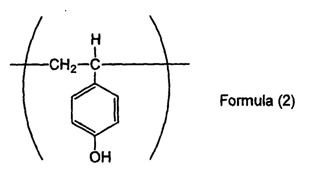
- the repeating unit represented by the Formula (2) is p-vinylphenol, and a homopolymer obtainable by the polymerization of such a repeating unit can be yielded by a conventional method. For instance, it can be obtained by streaming a solution prepared by dissolving p-hydroxystyrene monomer in propylene glycol (manufactured by LANCASTER Co., Ltd.) with nitrogen for 30 minutes, followed by addition of azobisisobutyronitrile (AIBN, manufactured by JUNSEI CHEMICAL Co., Ltd.) as a polymerization initiator while holding the reaction solution at 70°C, and stirring for 48 hours in a nitrogen atmosphere. A reactant can be collected as powder by reprecipitating it in one litter of distilled water.
- the weight-average molecular weight of this polymer is 1000 to 100000, preferably 1000 to 60000, further preferably 1000 to 30000. In addition, such a polymer is also commercially available.
- the homopolymer comprised of the repeating unit represented by the Formula (3) is one in which a hydrogen atom at an ortho position and/or a meta position of the benzene ring of p-vinylphenol is substituted with one and a half bromine atoms in average per one unit of p-vinylphenol.
- the methods for obtaining the polymer include a method of brominating a homopolymer comprised of the repeating unit represented by the Formula (2). For instance, it can be obtained by dissolving the homopolymer comprised of the repeating unit represented by the Formula (2) in carbon tetrachloride or carbon bisulfide, followed by streaming the solution with nitrogen for 30 minutes, adding bromine in the solution at a room temperature, and stirring for 5 hours.
- a reactant can be collected as powder by reprecipitating it in one liter of distilled water.
- the weight-average molecular weight of this polymer is 1000 to 100000, preferably 1000 to 60000, further preferably 1000 to 30000.
- such a polymer can be also commercially available.
- a p-vinylphenol unit represented by the Formula (2) is a main component thereof containing 20% or more, preferably 20% to 80% of the repeating unit based on the total number of repeating units in the copolymer.
- such a copolymer can be obtained by dissolving commercially-available p-hydroxystyrene monomer and styrene monomer in propylene glycol, followed by streaming the reaction solution with nitrogen for 30 minutes, adding azobisisobutyronitrile (AIBN) as a polymerization initiator, and stirring for 48 hours in a nitrogen atmosphere while maintaining the reaction solution at 70°C.
- AIBN azobisisobutyronitrile
- a reactant can be collected as powder by reprecipitating it in one liter of distilled water.
- the weight-average molecular weight of this polymer is 1000 to 100000, preferably 1000 to 60000, further preferably 1000 to 30000.
- such a polymer can be also commercially available.
- a p-vinylphenol unit is a main component thereof containing 20% or more, preferably 20% to 80% of the repeating unit based on the total number of repeating units in the copolymer.
- such a copolymer can be obtained by dissolving commercially-available p-hydroxystyrene monomer and methyl methacrylate in propylene glycol, followed by streaming the reaction solution with nitrogen for 30 minutes, adding azobisisobutyronitrile (AIBN) as a polymerization initiator, and stirring for 48 hours in a nitrogen atmosphere while maintaining the reaction solution at 70°C.
- AIBN azobisisobutyronitrile
- a reactant can be collected as powder by reprecipitating in one liter of distilled water.
- the weight-average molecular weight of this polymer is 1000 to 100000, preferably 1000 to 60000, further preferably 1000 to 30000.
- such a polymer can be also commercially available.
- a p-vinylphenol unit represented by the Formula (2) is a main component thereof containing 20% or more, preferably 20% to 80% of the repeating unit based on the total number of repeating units in the copolymer.
- such a copolymer can be obtained by dissolving commercially-available p-hydroxystyrene monomer and 2-hydroxyethyl methacrylate in propylene glycol, followed by streaming the reaction solution with nitrogen for 30 minutes, adding azobisisobutyronitrile (AIBN) as a polymerization initiator, and stirring for 48 hours in a nitrogen atmosphere while maintaining the reaction solution at 70°C.
- a reactant can be collected as powder by reprecipitating it in one liter of distilled water.
- the weight-average molecular weight of this polymer is 1000 to 100000, preferably 1000 to 60000, further preferably 1000 to 30000.
- such a polymer can be also commercially available.
- a p-vinylphenol unit represented by the Formula (2) is a main component thereof containing 20% or more, preferably 20% to 80% of the repeating unit based on the total number of repeating units in the copolymer.
- such a copolymer can be obtained by dissolving commercially-available p-hydroxystyrene monomer and butyl methacrylate in propylene glycol, followed by streaming the reaction solution with nitrogen for 30 minutes, adding azobisisobutyronitrile (AIBN) as a polymerization initiator, and stirring for 48 hours in a nitrogen atmosphere while maintaining the reaction solution at 70°C.
- AIBN azobisisobutyronitrile
- a reactant can be collected as powder by reprecipitating it in one liter of distilled water.
- the weight-average molecular weight of this polymer is 1000 to 100000, preferably 1000 to 60000, further preferably 1000 to 30000.
- such a polymer can be also commercially available.
- poly p-vinylphenol bromide of poly p-vinylphenol, copolymer of p-vinylphenol and styrene, copolymer of p-vinylphenol and methyl methacrylate, copolymer of p-vinylphenol and 2-hydroxyethyl methacrylate, and copolymer of p-vinylphenol and butyl acrylate are preferable.
- Each of these polymers has a glass transition temperature of 100 to 170°C.
- the composition for forming a gap-filling material for lithography of the present invention is allowed to contain a cross-linking agent having at least two cross-linking forming functional groups.
- the cross-linking agents include melamines, substituted ureas, polymers that contain epoxy groups and so on. Among them, a preferable compound is methoxymethylated glycoluril, methoxymethylated melamine, or the like, and a more preferable compound is tetramethoxymethyl glycoluril or hexamethoxymethylol melamine.
- the addition amount of the cross-linking agent varies depending on the application solvent to be used, the base substrate to be used, the desired viscosity of the solution, the desired shape of the coating, and so on, it is 0.001 to 20 parts by weight, preferably 0.01 to 10 parts by weight, further preferably 0.1 to 5.0 parts by weight per 100 parts by weight of the whole composition.
- the composition for forming a gap-filling material for lithography of the present invention is allowed to contain a cross-linking catalyst.
- the cross-linking catalysts include compounds capable of regulating the progression of a cross-linking reaction, such as a compound that generates an acid by heat and a compound that generates an acid by light.
- preferable compounds are a p-toluenesulfonic acid, a pyridium p-toluenesulfonic acid and so on.
- the addition amount of the cross-linking catalyst varies depending on the application solvent to be used, the ground substrate to be used, the desired viscosity of the solution, the desired shape of the coating, and so on, it is 0.01 to 30 parts by weight, preferably 0.1 to 30 parts by weight, further preferably 0.5 to 20 parts by weight per 100 parts by weight of the addition amount of the cross-linking agent.
- the solvents which can be used for dissolving the polymer include ethylene glycol monomethylether, ethylene glycol monoethyl ether, methyl cellosolve acetate, ethyl cellosolve acetate, diethylene glycol monomethylether, diethylene glycol monoethyl ether, diethylene glycol monobutyl ether, propylene glycol, propylene glycol monomethylether, propylene glycol monoethyl ether, propylene glycol monobutyl ether, propylene glycol monomethylether acetate, propylene glycol propyl ether acetate, toluene, xylene, methylethyl ketone, cyclopentanone, cyclohexanone, ethyl 2-hydroxypropionate, ethyl 2-hydroxy-2-methyl propionate, ethyl ethoxyacetate, ethyl hydroxy
- the solvent to be used in a polymer solution of the composition for forming gap-filling material for lithography of the present invention may preferably contain at least a solvent (s) having a boiling point higher than a glass transition temperature of the above-mentioned polymer.
- the solvent (s) may preferably have a boiling point 10°C or more higher than the glass transition temperature of the polymer.
- the boiling points of these solvents may preferably be in the range of 145°C to 220°C.
- the solvents (s) that satisfy these conditions include propylene glycol monomethylether, propylene glycol monobutyl ether, butyl lactate, diethylene glycol monomethylether, cyclohexanone, propylene glycol monomethylether acetate and so on.
- butyl lactate, propylene glycol monobutyl ether, propylene glycol monomethylether acetate, cyclohexanone, diethylene glycol monomethylether, or any mixture thereof is preferable.
- composition for forming a gap-filling material for lithography of the present invention may further contain a rheology adjusting agent, a co-adhesive agent, a surfactant and so on if required.
- the rheology adjusting agent is added to improve the flow properties of the composition for forming gap-filling material for lithography. Particularly, in the step of baking, it is added for the purpose of improving the filling property of the composition for forming a gap-filling material for lithography into the inside of the hole.
- the rheology adjustor include phthalic acid derivatives of dimethyl phthalate, diethyl phthalate, diisobutyl phthalic acid, dihexyl phthalate, and butyl isodecyl phthalate, adipate derivatives such as dinormalbutyl adipate, diisobutyl adipate, diisooctyl adipate and octyldecyl adipate, maleic acid derivatives such as dinormalbutyl malate, diethyl malate and dinonyl malate, oleic acid derivatives such as methyl oleate, butyl oleate and tetrahydrofurfuryl oleate, or stearic acid derivatives such as normal butyl stearate and glyceryl stearate.
- These rheology adjusting agents may be normally compounded in the proportions of less than 30 parts by weight based on 100 parts by weight of the composition
- the co-adhesive agent is added to improve the adhesion between the substrate or resist and the composition for forming gap-filling material for lithography and to prevent the resist pattern collapse, especially in the development.
- the co-adhesive agents include chlorosilanes such as trimethyl chlorosilane, dimethylvinyl chlorosilane, methyldiphenyl chlorosilane, and chloromethyl dimethyl chlorosilane and so on, alkoxy silanes such as trimethyl methoxy silane, dimethyl diethoxy silane, methyl dimethoxy silane, dimethyl vinylethoxy silane, diphenyl dimethoxy silane, phenyl triethoxy silane and so on, silazanes such as hexamethyl disilazane, N,N'-bis(trimethylsilane) urea, dimethyl trimethylsilyl amine, trimethylsilyl imidazole and so on, silanes such as vinyl trichlorosilane
- a surfactant may be compounded to prevent the generation of pin hole, striation or the like and to further improve thickness uniformity of the various location on the substrate.
- the surfactants include, for example, nonionic surfactants such as polyoxyethylene alkyl ethers including polyoxyethylene lauryl ether, polyoxyethylene stearyl ether, polyoxyethylene cetyl ether, polyoxyethylene oleyl ether and so on, polyoxyethylene alkylallyl ethers including polyoxyethylene octylphenol ether, polyoxyethylene nonylphenol ether, and so on, polyoxyethylene/polyoxypropylene block copolymers, sorbitan fatty acid esters including sorbitan monolaurate, sorbitan monopalmitate, sorbitan monostearate, sorbitan monooleate, sorbitan trioleate, sorbitan tristearate, and so on, polyoxyethylene
- Amount of these surfactants to be compounded is normally less than 0.2 parts by weight, preferably less than 0.1 parts by weight based on 100 parts by weight of the total composition of the present invention.
- These surfactants may be added solely or may be added as any combination of two or more surfactants.
- Either of negative- or positive-type resist can be used as resist coated over the top layer of the composition for forming a gap-filling material for lithography of the present invention.
- the resists include a positive-type resist including a novolac resin or 1,2-naphthoquinone diazidesulfonic acid ester, a chemical amplification type resist comprised of a photo-acid generator and a binder having a group which can increase alkaline dissolving speed by the decomposition with an acid, a chemical amplification type resist comprised of an alkali-soluble binder, a photo-acid generator and a low-molecular weight compound which can increase decomposition with an acid to increase alkaline dissolving speed of resist, a chemical amplification type resist comprised of a photo-acid generator, a binder having a group which can increase the alkaline dissolving speed by the decomposition with an acid and a low-molecular weight compound which can increase the alkaline dissolving
- the developers which can be used for the positive type photoresist coated over a gap-filling material for lithography formed with the use of the composition for forming a gap-filling material for lithography of the present invention may be alkaline aqueous solutions of: inorganic alkalines such as sodium hydroxide, potassium hydroxide, sodium carbonate, sodium silicate, sodium metasilicate, aqueous ammonia and so on; primary amines such as ethyl amine, n-propyl amine and so on; secondary amines such as diethyl amine, dinormalbutyl amine and so on; tertiary amines such as triethyl amine, methyl diethyl amine and so on; alcohol amines such as dimethylethanol amine, triethanol amine and so on; quaternary ammonium salts such as tetramethyl ammonium hydroxide, tetraethyl ammonium hydroxide, choline and so on; cycl
- alcohols such as isopropyl alcohol, anionic surfactant and the like, and so on may be used by adding proper quantity thereof to the alkaline aqueous solution.
- a preferable developer is the quaternary ammonium salt, more preferably tetramethyl ammonium hydroxide and choline.
- a semiconductor device can be manufactured by forming an integrated circuit element by transferring an image on a substrate by a method comprising:
- a composition for forming a gap-filling material for lithography is applied to a substrate to be used in the production of a precision integrated circuit element (e.g., a transparent substrate such as silicon/silicon dioxide coating, silicon nitride coating, glass substrate, ITO substrate and so on) by an appropriate application method such as one using a spinner or a coater, followed by baking and curing to obtain a gap filling material.
- a precision integrated circuit element e.g., a transparent substrate such as silicon/silicon dioxide coating, silicon nitride coating, glass substrate, ITO substrate and so on
- the gap filling material may have a film thickness of 0.01 to 3.0 ⁇ m and the baking conditions may be at 60°C to 250°C for 0.3 to 120 minutes.
- a bottom anti-reflective coating is coated and is then baked and cured to form a bottom anti-reflective coating. Furthermore, a photoresist is applied and is then exposed through a predetermined mask, followed by developing, rinsing and drying to produce a semiconductor device. If required, two stages of baking with different temperatures and post exposure baking (PEB) may be performed.
- PEB post exposure baking
- a composition for forming a gap-filling material for lithography can be obtained by forming a bottom anti-reflective coating made of an inorganic material on a substrate to be used in the production of a precision integrated circuit element (e.g., a transparent substrate such as silicon/silicon dioxide coating, silicon nitride coating, glass substrate, and ITO substrate) by, for example, the CDV method, and applying a composition for forming a gap-filling material for lithography thereon by an appropriate application method such as one using a spinner or a coater, followed by baking and curing to obtain a gap-filling material for lithography.
- a precision integrated circuit element e.g., a transparent substrate such as silicon/silicon dioxide coating, silicon nitride coating, glass substrate, and ITO substrate
- an appropriate application method such as one using a spinner or a coater
- the gap filling material may have a film thickness of 0.01 to 3.0 ⁇ m and the baking conditions may be at 60°C to 250°C for 0.3 to 120 minutes. Subsequently, a photoresist is coated and is then exposed through a predetermined mask, followed by developing, rinsing, and drying to produce a superior semiconductor device. If required, two stages of baking with different temperatures and post exposure baking may be performed.
- a substrate having holes can be favorably planarized by means of the composition for forming a gap-filling material of the present invention.
- the polymer to be used in the composition for forming a gap-filling material of the present invention there is introduced no aromatic group having a light-absorbency such as is present in the polymer to be used in the composition for forming a bottom anti-reflective coating, thus realizing a larger dry etching rate.
- it has a larger dry-etching ability as compared with that of the photoresist to be coated on the upper layer and, as the case may be, as compared with that of the bottom anti-reflective coating. Therefore, a film thickness of the resist can be reduced and a fine image can be transferred to the substrate.
- the glass transfer temperature (Tg) for a polymer to be used is lowered a little to provide it with a fluidity at the time of baking while making it become insoluble to the resist solvent after complete solidification.
- Tg glass transfer temperature
- planarizing there may be conceived a various kinds of methods including those concerned with the polymerization degree of the polymer, the concentration of the polymer having cross-linking points in the composition, the percentage of the polymers having cross-linking points in the total solids, the selection of additive components and so on.
- the resulting sediment was filtrated and was then dried to obtain powder of the polymer.
- the resulting polymer was subjected to a GPC analysis. As a result, the weight-average molecular weight of the resulting polymer was 3000 in terms of the standard polystyrene (60% yield).
- the structure of the resulting polymer was of a copolymerization of p-vinylphenol and styrene at a molar ratio of 70 : 30.
- the resulting sediment was filtrated and was then dried to obtain powder of the polymer.
- the resulting polymer was subjected to a GPC analysis. As a result, the weight-average molecular weight of the resulting polymer was 5300 in terms of the standard polystyrene.
- the structure of the resulting polymer was of a copolymerization of p-vinylphenol and methyl methacrylate at a molar ratio of 49:51.
- the glass transition temperature of the polymer was 135°C.
- the coefficient H defined as [logarithmic change in viscosity (mPas)] / [change in solid content concentration (% by weight)] was 0.046 under the measurement conditions of a solvent temperature of 25°C and a solid content concentration of 8.3 to 25% by weight.
- the resulting polymer was polyacrylic acid.
- the coefficient H defined as [logarithmic change in viscosity (mPas) ] / [change in solid content concentration (% by weight)] was 0.069 under the measurement conditions of a solvent temperature of 25°C and a solid content concentration of 8.3 to 25% by weight.
- the solution was reprecipitated in distilled water to obtain a sediment.
- the sediment was filtrated and dried to obtain fine particles of the polymer.
- the resulting polymer was subjected to a GPC analysis. As a result, the weight-average molecular weight of the polymer was 130000 in terms of the standard polystyrene.
- the resulting polymer was polyhydroxypropyl methacrylate. Furthermore, 1 g of the obtained polyhydroxypropyl methacrylate was dissolved in 3 g of propylene glycol monomethylether to prepare a 25 w/t% solution thereof. The viscosity of the solution measured by an E-type rotational viscometer was 225 mPas at 25°C.
- the given solution was filtered through a micro-filter made by polyethylene with a pore size of 0.05 ⁇ m to prepare a composition for forming a gap-filling material.
- the resulting composition was subjected to a GPC analysis and the weight-average molecular weight thereof was 6000 in terms of the standard polystyrene.
- MARUKA LYNCUR MB was dissolved in 3 g of propylene glycol monomethylether to prepare a 25 w/t% solution thereof.
- the viscosity of the solution measured by an E-type rotational viscometer was 7.6 mPas at 25°C.
- the coefficient H defined as [logarithmic change in viscosity (mPas)] / [change in solid content concentration (% by weight)] was 0.029 under the measurement conditions of a solvent temperature of 25°C and a solid content concentration of 8.3 to 25% by weight.
- the given solution was filtered through a micro-filter made by polyethylene with a pore diameter of 0.05 ⁇ m to prepare a composition for forming a gap-filling material for lithography.
- the resulting composition was subjected to a GPC analysis and the weight-average molecular weight thereof was 6000 in terms of the standard polystyrene.
- RESITOP PSM-4326 was dissolved in 3 g of propylene glycol monomethylether to prepare a 25 w/t% solution thereof.
- the viscosity of the solution measured by an E-type rotational viscometer was 31.9 mPas at 25°C.
- the coefficient H defined as [logarithmic change in viscosity (mPas)] / [change in solid content concentration (% by weight)] was 0.053 under the measurement conditions of a solvent temperature of 25°C and a solid content concentration of 8.3 to 25% by weight.
- compositions for forming a gap-filling material for lithography obtained in Examples 1 to 11 and Comparative Examples 1 to 5 were applied over the respective silicon wafers by a spinner and were then heated on a hot plate at 205°C for 1 minute to form their respective gap-filling materials for lithography (0.22 ⁇ m in film thickness).
- the gap-filling materials for lithography were dipped in solvents to be used for resist, for example, ethyl lactate and propylene glycol monomethylether to confirm that they were insoluble in these solvents.
- compositions for forming a gap-filling material for lithography obtained in Examples 1 to 11 and Comparative Examples 1 to 5 were applied to the respective silicon wafers by a spinner and were then heated on a hot plate at 205°C for 1 minute to form their respective gap-filling materials for lithography (0.22 ⁇ m in film thickness).
- a commercially-available resist solution (APEX-E, manufactured by Shipley Company) was applied to the top layer of the gap-filling material for lithography by the spinner and was then heated on the hot plate at 90°C for 1 minute. After exposing the resist, a post-exposure baking was performed at 90°C for 1.5 minutes. After developing the resist, the film thickness of the gap-filling material for lithography was measured to confirm that there was no intermixing between the gap-filling materials for lithography obtained in Examples 1 to 4 and Comparative Example 1 and the resist layer.
- compositions for forming a gap-filling material for lithography obtained in Examples 1 to 4 and Comparative Example 1 were applied over the respective silicon wafer substrates having holes (0.25 ⁇ m in diameter and 0.9 ⁇ m in depth) by a spinner and were then heated on a hot plate at 205°C for 1 minute to form their respective gap-filling materials for lithography (0.24 ⁇ m in film thickness).
- planarizing factor was evaluated by observing the cross-sectional shape of the obtained substrate using a scanning electron microscopy (SEM).
- SEM scanning electron microscopy
- Planarizing factor [1 - a/b] x 100
- the substrate used is a silicon wafer substrate having holes in Iso and Dense patterns as illustrated in Fig. 1.
- the Iso pattern is one in which the distance from the center of a hole to the center of the adjacent hole is three times larger than the diameter of the hole.
- the Dense pattern is one in which the distance from the center of a hole to the center of the adjacent hole is equal to the diameter of the hole.
- the depth of the hole was 0.9 ⁇ m and the diameter of the hole was 0.25 ⁇ m.
- the film thickness of each portion of the substrate formed by the composition for forming a gap-filling material for lithography was measured.
- the planarizing factor of the film obtained by each of the compositions for forming a gap-filling material for lithography of Examples 1 to 4 was larger than that of Comparative Example 1, with particularly excellent planarizing ability in Dense pattern that requires severe conditions. Furthermore, the difference between the film thickness of the Iso portion and that of the Dense portion was small in each of the compositions for forming a gap-filling material for lithography of Examples 1 to 4. This indicates that the compositions for forming a gap-filling material were smoothly poured into a plurality of holes also in the Dense portion in which the number of holes per unit area on the hole substrate (the hole density) is larger than that of the (sob portion. It is considered that this has led to a small difference between the film thickness of the Iso portion and that of the Dense portion and to a large planarizing factor.
- each of the compositions for forming a gap-filling material for lithography was subjected to the measurements of its viscosity (mPas) and coefficient H, where the coefficient H was defined as [logarithmic change in viscosity (mPas)] /[change in solid content concentration (% by weight)] under the measurement conditions in which the temperature of the solution was 25°C and the solid content concentration was 8.3 to 25% by weight. The manner thereof is shown in Fig. 2.
- planarizing factor of the film obtained from each of the compositions for forming a gap-filling material for lithography of Examples 1 to 3, 5, and 6 was larger than those of Comparative Examples 2 and 3, and in particular the planarizing ability thereof in the Dense patterns was excellent. It is considered that this is caused by an increase in fluidity of the solution in the steps of spinning and baking as the viscosity of the composition for forming a gap-filling material becomes lower.
- the planarizing factor of the film obtained from the composition for forming a gap-filling material for lithography of each of Examples 7 to 11 was high as compared with that of the film obtained from each of Comparative Examples 4 and 5 and in particular the planarizing ability thereof was excellent in the Dense patterns that requires severe conditions.
- the gap-filling material was adhered along the step in the substrate (a conformal type).
- each of Examples 7 to 11 it is considered that the difference in planarizing factor is small as the composition for forming a gap-filling material flows into a plurality of holes with a larger fluidity also in the Dense portion where the number of holes per unit area on the substrate is larger than that of the Iso portion.
- the reason why the compositions for forming a gap-filling material of Examples 7 to 11 have planarizing factors larger than those of Comparative Examples 4 to 5 is that each of them contains a solvent having a boiling point higher than the glass transition temperature of the polymer or the boiling point of such a solvent is in the range of 145°C to 220°C.
- a gap-filler forming composition of the present invention planarizes the substrate having holes by filling in the irregularities thereof and finds utility in the improvement of uniformity of the film thickness of an applied film such as a photoresist applied on the substrate. It has a high dry etching rate as compared with that of a photoresist layer and it does not cause an intermixing with the photoresist layer. In addition, there is no diffusant into the photoresist at the time of heating and drying. Therefore, a lithographic gap-filler having a high resolution and an excellent dependency on the film thickness of the photoresist can be obtained and an excellent resist-pattem forming process can be provided.
Landscapes
- Chemical & Material Sciences (AREA)
- Physics & Mathematics (AREA)
- General Physics & Mathematics (AREA)
- Engineering & Computer Science (AREA)
- Organic Chemistry (AREA)
- Architecture (AREA)
- Structural Engineering (AREA)
- Wood Science & Technology (AREA)
- Materials Engineering (AREA)
- Life Sciences & Earth Sciences (AREA)
- Health & Medical Sciences (AREA)
- Chemical Kinetics & Catalysis (AREA)
- Medicinal Chemistry (AREA)
- Polymers & Plastics (AREA)
- Spectroscopy & Molecular Physics (AREA)
- Materials For Photolithography (AREA)
- Addition Polymer Or Copolymer, Post-Treatments, Or Chemical Modifications (AREA)
- Macromonomer-Based Addition Polymer (AREA)
Abstract
Description


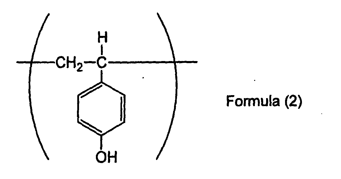


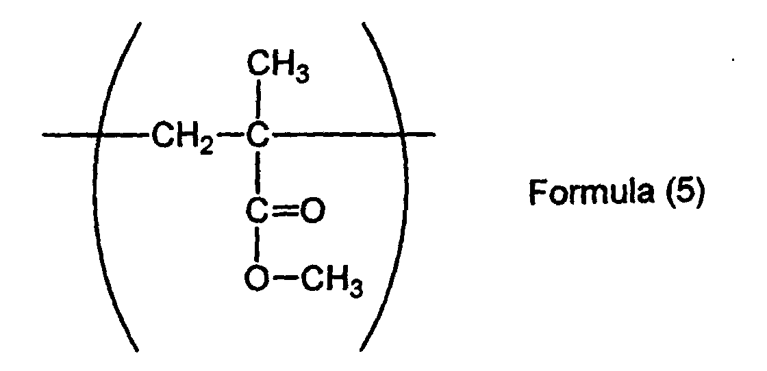
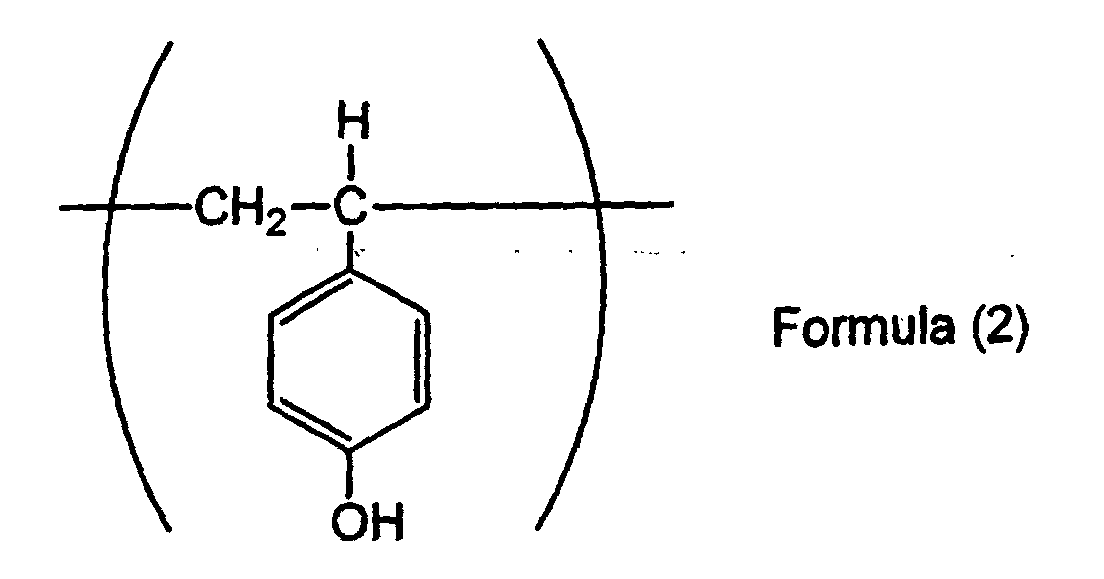


Fig. 2 is a graph that represents a relationship between a concentration (% by weight) and viscosity (mPas) of a polymer solution used in Examples and Comparative Examples, where concentration values are plotted on the lateral axis and viscosity values measured at 25°C are plotted in common logarithm on the vertical axis. In the figure, 1 ○ is a straight line that denotes a coefficient H of Example 1 and Example 2, 2 ○ is a straight line that denotes the coefficient H of Example 3, 3 ○ is a straight line that denotes the coefficient H of Example 5, 4 ○ is a straight line that denotes the coefficient H of Example 6, 5 ○ is a straight line that denotes the coefficient H of Comparative Example 2, and 6 ○ is a straight line that denotes the coefficient H of Comparative Example 3.
m-chlorobenzaldehyde, p-chlorobenzaldehyde, o-nitrobenzaldehyde,
m-nitrobenzaldehyde, p-nitrobenzaldehyde, o-methylbenzaldehyde,
m-methylbenzaldehyde, p-methylbenzaldehyde, o-ethylbenzaldehyde,
m-ethylbenzaldehyde, p-ethylbenzaldehyde, p-normal butyl aldehyde, furfural, 1-naphtoaldehyde, 2-naphtoaldehyde and 2-hydroxy-1-naphtoaldehyde. Among them, formaldehyde is specifically preferable.
N-arylmethacrylamide, N,N-dialkylmethacrylamide, N,N-diarylmethacrylamide, N-methyl-N-phenylmethacrylamide, and N-ethyl-N-phenylmethacrylamide.
Furthermore, 1 g of the obtained polyhydroxypropyl methacrylate was dissolved in 3 g of propylene glycol monomethylether to prepare a 25 w/t% solution thereof. The viscosity of the solution measured by an E-type rotational viscometer was 225 mPas at 25°C.

The coefficient H defined as [logarithmic change in viscosity (mPas)] / [change in solid content concentration (% by weight)] was 0.053 under the measurement conditions of a solvent temperature of 25°C and a solid content concentration of 8.3 to 25% by weight.
| Film thickness (Unit:nm) | Planarizing factor (Unit:%) | |||||
| Iso | Dense | Bias | Iso | Dense | Bias | |
| Example 1 | 190 | 80 | 110 | 98 | 93 | 5 |
| Example 2 | 200 | 100 | 100 | 96 | 91 | 5 |
| Example 3 | 180 | 90 | 90 | 98 | 94 | 4 |
| Example 4 | 180 | 100 | 80 | 89 | 81 | 8 |
| Comparative Example 1 | 200 | 80 | 120 | 84 | 53 | 31 |
| Coefficient H | Viscosity of the polymer solution (Unit:mPa·s) | Planarizing factor (Unit:%) | |||
| Iso | Dense | Bias | |||
| Example 1 | 0.041 | 15 | 98 | 93 | 5 |
| Example 2 | 0.041 | 15 | 96 | 91 | 5 |
| Example 3 | 0.029 | 8 | 98 | 94 | 4 |
| Example 5 | 0.046 | 21 | 98 | 97 | 1 |
| Example 6 | 0.053 | 32 | 89 | 84 | 5 |
| Comparative Example 2 | 0.069 | 98 | 88 | 72 | 15 |
| Comparative Example 3 | 0.079 | 225 | 82 | 51 | 31 |
| Planarizing factor (Unit: nm) | |||
| Iso | Dense | Bias | |
| Example 7 | 97 | 94 | 3 |
| Example 8 | 96 | 91 | 5 |
| Example 9 | 97 | 95 | 2 |
| Example 10 | 91 | 73 | 18 |
| Example 11 | 90 | 60 | 30 |
| Comparative Example 4 | 87 | 32 | 55 |
| Comparative Example 5 | 89 | 45 | 44 |
Claims (21)
- A composition for forming a gap-filling material to be used in production of a semiconductor device by a method of applying a resist for coating onto a substrate having holes where an aspect ratio defined as height/diameter is 1 or more and transferring an image on the substrate using a lithographic process, which is applied to the substrate prior to the coating with the resist so as to planarize the surface of the substrate, characterized by containing a polymer solution comprised of a polymer and a solvent.
- The composition for forming a gap-filling material according to the claim 1, characterized in that the polymer solution has a coefficient H of 0.06 or less, which is defined as [logarithmic change in viscosity (mPas)] / [change in solid content concentration (% by weight)], and a viscosity of 1 to 80 mPas, which is measured at a solid content concentration of 25% by weight.
- The composition for forming a gap-filling material according to the claim 1 or 2, characterized in that the polymer solution contains 0.1 to 30% by weight of solid content.
- The composition for forming a gap-filling material according to one of the claims 1 to 3, characterized in that the solvent contains 20% by weight or more of a solvent (s) having a boiling point higher than a glass transition temperature of the polymer based on the whole solvent.
- The composition forming a gap-filling material according to the claim 4, characterized in that the boiling point of the solvent (s) is 10°C or more higher than the glass transition temperature of the polymer.
- The composition for forming a gap-filling material according to one of the claims 1 to 5, characterized in that the boiling point of the solvent (s) is from 145 to 220°C.
- The composition for forming a gap-filling material according to one of the claims 1 to 6, characterized in that the solvent (s) is butyl lactate, propylene glycol monobutyl ether, propylene glycol monomethylether acetate, cyclohexanone, diethylene glycol monomethylether, or any mixture thereof.
- The composition for forming a gap-filling material according to the claims 1 to 7, characterized in that a weight-average molecular weight of the polymer is from 500 to 30000.
- The composition for forming a gap-filling material according to one of the claims 1 to 8, characterized in that the polymer comprises at least one repeating unit represented by the following Formula (1):[wherein R1 and R2 each independently represent a hydrogen atom, a methyl group, a fluorine atom, a chlorine atom, a bromine atom or a cyano group].

- The composition for forming a gap-filling material according to the claim 9, characterized in that the polymer is a homopolymer comprised of the repeating unit represented by the Formula (1), or a copolymer comprised of the repeating unit represented by the Formula (1) and a repeating unit which is a vinyl group that contains an aromatic moiety or a carboxylic acid ester moiety on a side chain thereof.
- The composition for forming a gap-filling material according to the claim 10, characterized in that the polymer is poly p-vinylphenol that comprises a repeating unit represented by the following Formula (2):
- The composition for forming a gap-filling material according to the claim 10, characterized in that the polymer is a bromide of poly p-vinylphenol, which comprises a repeating unit represented by the following Formula (3):

- The composition for forming a gap-filling material according to the claim 10, characterized in that the polymer is a copolymer of p-vinylphenol and styrene, which comprises a repeating unit represented by the following Formula (2):and a repeating unit represented by the following Formula (4):
 and in which 20% or more of the repeating unit represented by the Formula (2) is contained based on the total number of the repeating units in the polymer.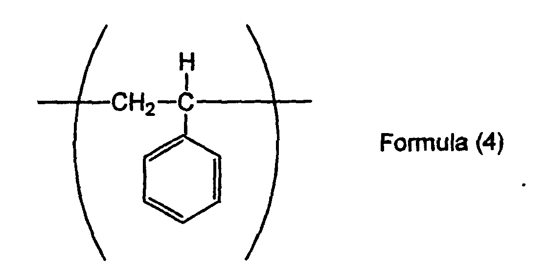
- The composition for forming a gap-filling material according to the claim 10, characterized in that the polymer is a copolymer of p-vinylphenol and methyl methacrylate, which comprises a repeating unit represented by the following Formula (2):and a repeating unit represented by the following Formula (5):
 and in which 20% or more of the repeating unit represented by the Formula (2) is contained based on the total number of the repeating units in the polymer.
- The composition for forming a gap-filling material according to the claim 10, characterized in that the polymer is a copolymer of p-vinylphenol and 2-hydroxyethyl methacrylate, which comprises a repeating unit represented by the following Formula (2):and a repeating unit represented by the following Formula (6):
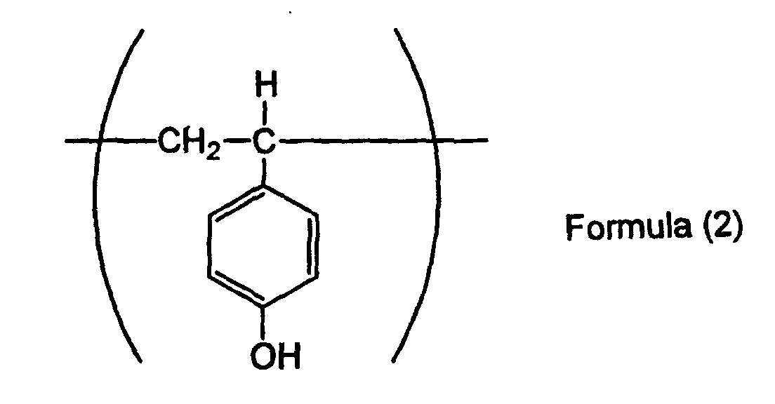 and in which 20% or more of the repeating unit represented by the Formula (2) is contained based on the total number of the repeating units in the polymer.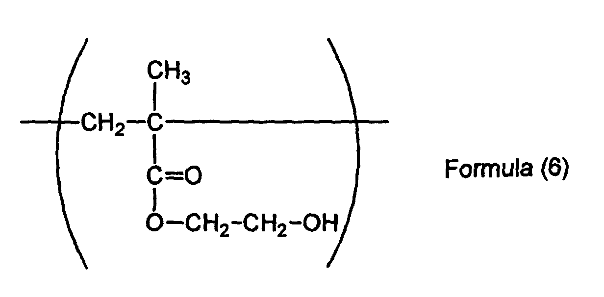
- The composition for forming a gap-filling material according to the claim 10, characterized in that the polymer is a copolymer of p-vinylphenol and butyl acrylate, which comprises a repeating unit represented by the following Formula (2):and a repeating unit represented by the following Formula (7):
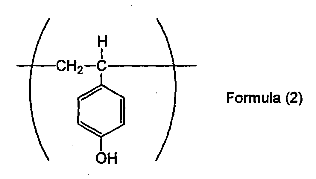 and in which 20% or more of the repeating unit represented by the formula (2) is contained based on the total number of the repeating units in the polymer.
- The composition for forming a gap-filling material according to one of the claims 1 to 16, characterized by further comprising a cross-linking agent having at least two cross-linking forming functional groups.
- A method of using a composition for forming a gap-filling material according to one of the claims 1 to 17, characterized in that the gap-filler forming composition is applied onto a substrate and is then baked in a lithographic process in production of a semiconductor device.
- The method of manufacturing a semiconductor device forming an integrated circuit element by transferring an image on a substrate, characterized by comprising:a step (A) in which the composition for forming a gap-filling material containing a polymer solution comprised of a polymer and a solvent is applied to a substrate having holes with an aspect ratio of 1 or more, which is defined as height/diameter, and is then dried to form a planarized filling layer on the substrate;a step (B) in which a resist is applied and dried; anda step (C) in which an exposure, a development, and an etching are performed.
- The method of manufacturing a semiconductor device according to the claim 19, characterized in that the composition for forming a gap-filling material used in the step (A) is a composition according to the claims 1 to 17.
- The method of manufacturing a semiconductor device according to the claim 19, characterized by further comprising a step (A') where a bottom anti-reflective coating is formed before or after the formation of a filling layer using the composition for forming a gap-filling material in the step (A).
Applications Claiming Priority (7)
| Application Number | Priority Date | Filing Date | Title |
|---|---|---|---|
| JP2000210844 | 2000-07-12 | ||
| JP2000210844 | 2000-07-12 | ||
| JP2000298044 | 2000-09-29 | ||
| JP2000298044 | 2000-09-29 | ||
| JP2001167701 | 2001-06-04 | ||
| JP2001167701 | 2001-06-04 | ||
| PCT/JP2001/006045 WO2002005035A1 (en) | 2000-07-12 | 2001-07-12 | Lithographic gap-filler forming composition |
Publications (3)
| Publication Number | Publication Date |
|---|---|
| EP1315045A1 true EP1315045A1 (en) | 2003-05-28 |
| EP1315045A4 EP1315045A4 (en) | 2008-04-23 |
| EP1315045B1 EP1315045B1 (en) | 2012-09-05 |
Family
ID=27344024
Family Applications (1)
| Application Number | Title | Priority Date | Filing Date |
|---|---|---|---|
| EP01947988A Expired - Lifetime EP1315045B1 (en) | 2000-07-12 | 2001-07-12 | Lithographic gap-filler forming composition |
Country Status (7)
| Country | Link |
|---|---|
| US (1) | US7517633B2 (en) |
| EP (1) | EP1315045B1 (en) |
| JP (1) | JP4654544B2 (en) |
| KR (3) | KR100881831B1 (en) |
| CN (1) | CN100367111C (en) |
| TW (1) | TWI224239B (en) |
| WO (1) | WO2002005035A1 (en) |
Cited By (4)
| Publication number | Priority date | Publication date | Assignee | Title |
|---|---|---|---|---|
| EP1598703A4 (en) * | 2003-02-21 | 2006-04-26 | Nissan Chemical Ind Ltd | COMPOSITION CONTAINING ACRYLIC POLYMER FOR THE FORMATION OF HOLLOW FILLING LOADS FOR USE IN LITHOGRAPHY |
| US7361718B2 (en) * | 2002-12-26 | 2008-04-22 | Nissan Chemical Industries, Ltd. | Alkali-soluble gap fill material forming composition for lithography |
| EP1484645A4 (en) * | 2002-02-19 | 2008-12-17 | Nissan Chemical Ind Ltd | Composition for forming anti-reflection coating |
| EP2574407A1 (en) * | 2011-09-29 | 2013-04-03 | Fraunhofer-Gesellschaft zur Förderung der angewandten Forschung e.V. | Method for producing a coating of a substrate |
Families Citing this family (65)
| Publication number | Priority date | Publication date | Assignee | Title |
|---|---|---|---|---|
| JP2004101794A (en) * | 2002-09-09 | 2004-04-02 | Toray Ind Inc | Flattening composition for semiconductor device |
| JP4487489B2 (en) * | 2002-09-20 | 2010-06-23 | 三菱電機株式会社 | Embedding material and manufacturing method of semiconductor integrated circuit using the embedding material |
| GB2400245B (en) * | 2003-04-01 | 2005-09-28 | Power Gems Ltd | Ignition system for a high-frequency high-intensity discharge lamp system |
| CN101550265B (en) | 2003-04-02 | 2014-04-16 | 日产化学工业株式会社 | Composition for formation of underlayer film for lithography containing epoxy compound and carboxylic acid compound |
| CN1774673B (en) | 2003-04-17 | 2010-09-29 | 日产化学工业株式会社 | Porous lower layer film and lower layer film forming composition for forming porous lower layer film |
| JP2004342751A (en) * | 2003-05-14 | 2004-12-02 | Toshiba Corp | Slurry for CMP, polishing method, and method for manufacturing semiconductor device |
| EP1649322A4 (en) | 2003-07-17 | 2007-09-19 | Honeywell Int Inc | PLANARIZATION FILMS FOR ADVANCED MICROELECTRONIC DEVICES AND APPLICATIONS AND METHODS FOR PRODUCING SAID FILMS |
| TWI363251B (en) | 2003-07-30 | 2012-05-01 | Nissan Chemical Ind Ltd | Sublayer coating-forming composition for lithography containing compound having protected carboxy group |
| TWI360726B (en) * | 2003-10-30 | 2012-03-21 | Nissan Chemical Ind Ltd | Sublayer coating-forming composition containing de |
| JP3759526B2 (en) | 2003-10-30 | 2006-03-29 | 丸善石油化学株式会社 | Method for producing copolymer for semiconductor lithography |
| KR100586165B1 (en) * | 2003-12-30 | 2006-06-07 | 동부일렉트로닉스 주식회사 | Floor anti-reflective coating method |
| US9257302B1 (en) | 2004-03-25 | 2016-02-09 | Novellus Systems, Inc. | CVD flowable gap fill |
| US7524735B1 (en) | 2004-03-25 | 2009-04-28 | Novellus Systems, Inc | Flowable film dielectric gap fill process |
| US7582555B1 (en) | 2005-12-29 | 2009-09-01 | Novellus Systems, Inc. | CVD flowable gap fill |
| US7361455B2 (en) * | 2004-03-31 | 2008-04-22 | Intel Corporation | Anti-reflective coatings |
| JP4835854B2 (en) | 2004-07-02 | 2011-12-14 | 日産化学工業株式会社 | Lithographic underlayer film forming composition containing naphthalene ring having halogen atom |
| CN101048705B (en) * | 2004-11-01 | 2010-11-10 | 日产化学工业株式会社 | Underlayer film-forming composition for lithography containing cyclodextrin compound |
| CN101107569B (en) * | 2005-01-21 | 2011-06-15 | 日产化学工业株式会社 | Composition for forming of underlayer film for lithography that contains compound having protected carboxyl group |
| US8426111B2 (en) | 2005-04-19 | 2013-04-23 | Nissan Chemical Industries, Ltd. | Resist underlayer coating forming composition for forming photo-crosslinking cured resist underlayer coating |
| JP5062420B2 (en) | 2005-05-24 | 2012-10-31 | 日産化学工業株式会社 | Lithographic underlayer film forming composition comprising polysilane compound |
| KR100722984B1 (en) * | 2005-12-05 | 2007-05-30 | 제일모직주식회사 | Polymer for Semiconductor Fine Gap Fill and Composition for Semiconductor Fine Gap Fill |
| KR100717511B1 (en) * | 2005-11-02 | 2007-05-11 | 제일모직주식회사 | Polymer for semiconductor fine gap fill and composition using same |
| US8048615B2 (en) | 2005-12-06 | 2011-11-01 | Nissan Chemical Industries, Ltd. | Silicon-containing resist underlayer coating forming composition for forming photo-crosslinking cured resist underlayer coating |
| JP4784784B2 (en) | 2006-08-28 | 2011-10-05 | 日産化学工業株式会社 | Resist underlayer film forming composition containing liquid additive |
| JP5057107B2 (en) | 2006-10-12 | 2012-10-24 | 日産化学工業株式会社 | Manufacturing method of semiconductor device using four-layer laminate |
| WO2008047638A1 (en) | 2006-10-12 | 2008-04-24 | Nissan Chemical Industries, Ltd. | Process for semiconductor device production using under-resist film cured by photocrosslinking |
| US9245739B2 (en) | 2006-11-01 | 2016-01-26 | Lam Research Corporation | Low-K oxide deposition by hydrolysis and condensation |
| US7888273B1 (en) | 2006-11-01 | 2011-02-15 | Novellus Systems, Inc. | Density gradient-free gap fill |
| JP5588095B2 (en) | 2006-12-06 | 2014-09-10 | 丸善石油化学株式会社 | Copolymer for semiconductor lithography and method for producing the same |
| KR101446819B1 (en) | 2006-12-22 | 2014-10-01 | 마루젠 세끼유가가꾸 가부시키가이샤 | Method for manufacturing polymer for semiconductor lithography |
| US8334338B2 (en) | 2007-05-23 | 2012-12-18 | Jsr Corporation | Composition for forming resist lower layer film |
| CN101303525B (en) * | 2008-06-23 | 2012-12-05 | 上海集成电路研发中心有限公司 | Double-pattern exposure process |
| JP5591465B2 (en) | 2008-10-30 | 2014-09-17 | 丸善石油化学株式会社 | Method for producing copolymer solution for semiconductor lithography having uniform concentration |
| US8557712B1 (en) | 2008-12-15 | 2013-10-15 | Novellus Systems, Inc. | PECVD flowable dielectric gap fill |
| US8278224B1 (en) | 2009-09-24 | 2012-10-02 | Novellus Systems, Inc. | Flowable oxide deposition using rapid delivery of process gases |
| JP5504823B2 (en) * | 2009-10-28 | 2014-05-28 | Jsr株式会社 | Radiation-sensitive composition, protective film, interlayer insulating film, and method for forming them |
| WO2011072143A2 (en) | 2009-12-09 | 2011-06-16 | Novellus Systems, Inc. | Novel gap fill integration |
| US8685867B1 (en) | 2010-12-09 | 2014-04-01 | Novellus Systems, Inc. | Premetal dielectric integration process |
| US9719169B2 (en) | 2010-12-20 | 2017-08-01 | Novellus Systems, Inc. | System and apparatus for flowable deposition in semiconductor fabrication |
| WO2013035480A1 (en) * | 2011-09-09 | 2013-03-14 | 学校法人 関西大学 | Catalyst adsorption method and adsorption device |
| KR101922280B1 (en) * | 2011-10-12 | 2018-11-26 | 제이에스알 가부시끼가이샤 | Pattern forming method and composition for forming resist underlayer film |
| US8846536B2 (en) | 2012-03-05 | 2014-09-30 | Novellus Systems, Inc. | Flowable oxide film with tunable wet etch rate |
| CN102881642B (en) * | 2012-09-20 | 2018-04-06 | 上海集成电路研发中心有限公司 | The forming method of rewiring figure |
| US9927705B2 (en) | 2013-07-23 | 2018-03-27 | Nissan Chemical Industries, Ltd. | Additive for resist underlayer film-forming composition and resist underlayer film-forming composition containing the same |
| US9847222B2 (en) | 2013-10-25 | 2017-12-19 | Lam Research Corporation | Treatment for flowable dielectric deposition on substrate surfaces |
| KR102356815B1 (en) * | 2013-11-14 | 2022-01-27 | 롬 앤드 하스 일렉트로닉 머트어리얼즈 엘엘씨 | Gap-fill methods |
| JP6014110B2 (en) | 2013-12-23 | 2016-10-25 | ダウ グローバル テクノロジーズ エルエルシー | Gap filling method |
| US9324604B2 (en) | 2014-07-04 | 2016-04-26 | Rohm And Haas Electronic Materials Llc | Gap-fill methods |
| WO2016013344A1 (en) * | 2014-07-24 | 2016-01-28 | 日産化学工業株式会社 | Resin composition for forming color filter underlayer film |
| US10049921B2 (en) | 2014-08-20 | 2018-08-14 | Lam Research Corporation | Method for selectively sealing ultra low-k porous dielectric layer using flowable dielectric film formed from vapor phase dielectric precursor |
| US9508549B2 (en) | 2014-12-26 | 2016-11-29 | Dow Global Technologies Llc | Methods of forming electronic devices including filling porous features with a polymer |
| TWI592760B (en) * | 2014-12-30 | 2017-07-21 | 羅門哈斯電子材料韓國有限公司 | Coating compositions for use with an overcoated photoresist |
| KR101926294B1 (en) * | 2015-03-30 | 2018-12-06 | 미쓰이 가가쿠 가부시키가이샤 | METHOD FOR MANUFACTURING FLANGE FLATING FILM |
| US10388546B2 (en) | 2015-11-16 | 2019-08-20 | Lam Research Corporation | Apparatus for UV flowable dielectric |
| US9916977B2 (en) | 2015-11-16 | 2018-03-13 | Lam Research Corporation | Low k dielectric deposition via UV driven photopolymerization |
| WO2017150094A1 (en) * | 2016-03-02 | 2017-09-08 | 富士フイルム株式会社 | Method for producing planarization film, active light sensitive or radiation sensitive composition for forming planarization film, planarization film, and method for manufacturing electronic device |
| CN108713164B (en) * | 2016-03-09 | 2022-03-18 | 日产化学工业株式会社 | Composition for forming resist underlayer film and method for forming resist pattern using same |
| JP2017215561A (en) * | 2016-05-30 | 2017-12-07 | アーゼッド・エレクトロニック・マテリアルズ(ルクセンブルグ)ソシエテ・ア・レスポンサビリテ・リミテ | GAP FILLING COMPOSITION AND METHOD FOR FORMING PATTERN USING COMPOSITION COMPRISING POLYMER |
| US10329452B2 (en) * | 2016-06-21 | 2019-06-25 | Honeywell International Inc. | Materials and spin coating methods suitable for advanced planarization applications |
| JP2018025649A (en) | 2016-08-09 | 2018-02-15 | アーゼッド・エレクトロニック・マテリアルズ(ルクセンブルグ)ソシエテ・ア・レスポンサビリテ・リミテ | Lower antireflection film forming composition |
| KR102696454B1 (en) * | 2016-12-02 | 2024-08-22 | 삼성디스플레이 주식회사 | flexible glass article having a low bending curvature and method of making the same |
| KR102646166B1 (en) * | 2019-02-27 | 2024-03-11 | 동우 화인켐 주식회사 | Composition for hard mask |
| JP2022529056A (en) | 2019-04-19 | 2022-06-16 | ラム リサーチ コーポレーション | Rapid flash parsing during atomic layer deposition |
| JP7345317B2 (en) * | 2019-08-23 | 2023-09-15 | 東京応化工業株式会社 | Filler and substrate treatment method |
| CN115851004B (en) * | 2021-09-24 | 2023-12-12 | 宝山钢铁股份有限公司 | Coating liquid for heat-resistant notch type oriented silicon steel coating, oriented silicon steel plate and manufacturing method thereof |
Family Cites Families (27)
| Publication number | Priority date | Publication date | Assignee | Title |
|---|---|---|---|---|
| JPS6050939A (en) * | 1983-08-30 | 1985-03-22 | Toshiba Corp | Manufacture of semiconductor device |
| JPH0727216B2 (en) * | 1985-02-06 | 1995-03-29 | 株式会社日立製作所 | Pattern formation method |
| KR930010248B1 (en) | 1984-09-14 | 1993-10-15 | 가부시끼가이샤 히다찌세이사꾸쇼 | Pattern Formation Method |
| JPS6170720A (en) * | 1984-09-14 | 1986-04-11 | Hitachi Ltd | Method of forming pattern |
| JPS6256947A (en) * | 1985-09-06 | 1987-03-12 | Fujitsu Ltd | Composition for flattened layer for resist having two-layered structure |
| US4784936A (en) * | 1985-10-24 | 1988-11-15 | General Electric Company | Process of forming a resist structure on substrate having topographical features using positive photoresist layer and poly(vinyl pyrrolidone) overlayer |
| JPH01167767A (en) * | 1987-12-23 | 1989-07-03 | Kyocera Corp | Photosensitive body temperature controller |
| JPH05107767A (en) * | 1991-10-17 | 1993-04-30 | Tosoh Corp | Coating solution for level difference substrate |
| US5276126A (en) | 1991-11-04 | 1994-01-04 | Ocg Microelectronic Materials, Inc. | Selected novolak resin planarization layer for lithographic applications |
| US5756256A (en) * | 1992-06-05 | 1998-05-26 | Sharp Microelectronics Technology, Inc. | Silylated photo-resist layer and planarizing method |
| JP2951504B2 (en) * | 1992-06-05 | 1999-09-20 | シャープ株式会社 | Silylated flattening resist, flattening method, and integrated circuit device manufacturing method |
| JP2525314B2 (en) * | 1992-07-31 | 1996-08-21 | 花王株式会社 | Method and apparatus for measuring mixed fluid |
| JPH06170720A (en) * | 1992-12-02 | 1994-06-21 | Speedfam Co Ltd | Surface plate dressing device |
| JPH0756336A (en) * | 1993-06-07 | 1995-03-03 | Ajinomoto Co Inc | Resin composition |
| JPH07333854A (en) * | 1994-06-07 | 1995-12-22 | Fujitsu Ltd | Method for manufacturing semiconductor device |
| US5858547A (en) * | 1994-07-06 | 1999-01-12 | Alliedsignal, Inc. | Novolac polymer planarization films for microelectronic structures |
| KR100434133B1 (en) | 1995-07-14 | 2004-08-09 | 텍사스 인스트루먼츠 인코포레이티드 | Texas instruments incorporated |
| DE69703094T2 (en) | 1996-03-07 | 2001-05-03 | Clariant Finance (Bvi) Ltd., Road Town | THERMAL PROCESSING PROCESS OF POSITIVE PHOTORESIST COMPOSITION |
| US5985524A (en) * | 1997-03-28 | 1999-11-16 | International Business Machines Incorporated | Process for using bilayer photoresist |
| JPH1167767A (en) * | 1997-08-20 | 1999-03-09 | Sony Corp | Method for manufacturing semiconductor device |
| US6057239A (en) * | 1997-12-17 | 2000-05-02 | Advanced Micro Devices, Inc. | Dual damascene process using sacrificial spin-on materials |
| JP2000164701A (en) * | 1998-11-25 | 2000-06-16 | Mitsubishi Electric Corp | Method for manufacturing semiconductor device |
| US6316165B1 (en) | 1999-03-08 | 2001-11-13 | Shipley Company, L.L.C. | Planarizing antireflective coating compositions |
| US6365321B1 (en) * | 1999-04-13 | 2002-04-02 | International Business Machines Corporation | Blends of hydroxystyrene polymers for use in chemically amplified positive resist formulations |
| EP1048980B1 (en) * | 1999-04-28 | 2009-09-30 | Qimonda AG | Bottom resist |
| US6376149B2 (en) * | 1999-05-26 | 2002-04-23 | Yale University | Methods and compositions for imaging acids in chemically amplified photoresists using pH-dependent fluorophores |
| US6461717B1 (en) | 2000-04-24 | 2002-10-08 | Shipley Company, L.L.C. | Aperture fill |
-
2001
- 2001-07-09 JP JP2001207811A patent/JP4654544B2/en not_active Expired - Lifetime
- 2001-07-12 TW TW090117112A patent/TWI224239B/en not_active IP Right Cessation
- 2001-07-12 KR KR1020087004105A patent/KR100881831B1/en not_active Expired - Lifetime
- 2001-07-12 KR KR1020037000282A patent/KR100820012B1/en not_active Expired - Lifetime
- 2001-07-12 US US10/311,959 patent/US7517633B2/en not_active Expired - Lifetime
- 2001-07-12 EP EP01947988A patent/EP1315045B1/en not_active Expired - Lifetime
- 2001-07-12 WO PCT/JP2001/006045 patent/WO2002005035A1/en not_active Ceased
- 2001-07-12 KR KR1020087004104A patent/KR100875802B1/en not_active Expired - Lifetime
- 2001-07-12 CN CNB018125042A patent/CN100367111C/en not_active Expired - Lifetime
Cited By (5)
| Publication number | Priority date | Publication date | Assignee | Title |
|---|---|---|---|---|
| EP1484645A4 (en) * | 2002-02-19 | 2008-12-17 | Nissan Chemical Ind Ltd | Composition for forming anti-reflection coating |
| US7361718B2 (en) * | 2002-12-26 | 2008-04-22 | Nissan Chemical Industries, Ltd. | Alkali-soluble gap fill material forming composition for lithography |
| EP1586945A4 (en) * | 2002-12-26 | 2009-12-09 | Nissan Chemical Ind Ltd | COMPOSITION FOR FORMING A MATERIAL FOR FILLING ALKALINE-SOLUBLE SPACES FOR LITHOGRAPHY |
| EP1598703A4 (en) * | 2003-02-21 | 2006-04-26 | Nissan Chemical Ind Ltd | COMPOSITION CONTAINING ACRYLIC POLYMER FOR THE FORMATION OF HOLLOW FILLING LOADS FOR USE IN LITHOGRAPHY |
| EP2574407A1 (en) * | 2011-09-29 | 2013-04-03 | Fraunhofer-Gesellschaft zur Förderung der angewandten Forschung e.V. | Method for producing a coating of a substrate |
Also Published As
| Publication number | Publication date |
|---|---|
| US7517633B2 (en) | 2009-04-14 |
| EP1315045B1 (en) | 2012-09-05 |
| KR100820012B1 (en) | 2008-04-07 |
| JP4654544B2 (en) | 2011-03-23 |
| KR100881831B1 (en) | 2009-02-03 |
| US20030146416A1 (en) | 2003-08-07 |
| EP1315045A4 (en) | 2008-04-23 |
| WO2002005035A1 (en) | 2002-01-17 |
| KR20080028497A (en) | 2008-03-31 |
| KR20030079906A (en) | 2003-10-10 |
| CN100367111C (en) | 2008-02-06 |
| JP2003057828A (en) | 2003-02-28 |
| CN1440518A (en) | 2003-09-03 |
| KR20080027954A (en) | 2008-03-28 |
| TWI224239B (en) | 2004-11-21 |
| KR100875802B1 (en) | 2008-12-26 |
Similar Documents
| Publication | Publication Date | Title |
|---|---|---|
| US7517633B2 (en) | Composition for forming gap-filling material for lithography | |
| JP3918942B2 (en) | Antireflection film forming composition for lithography | |
| JP4488234B2 (en) | Coating type nitride film forming composition for hard mask | |
| CN101473270B (en) | Composition containing hydroxylated condensation resin for forming film under resist | |
| CN1768306B (en) | Underlayer film-forming composition for photolithography containing epoxy compound and carboxylic acid compound | |
| JP3985165B2 (en) | Antireflection film forming composition for lithography | |
| US7425403B2 (en) | Composition for forming anti-reflective coating for use in lithography | |
| JP3852593B2 (en) | Anti-reflective film forming composition | |
| KR101158297B1 (en) | Alkali-Soluble Gap Filling Material Forming Composition For Lithography | |
| JPWO2014007079A1 (en) | Method of manufacturing semiconductor device using organic underlayer film forming composition for solvent development lithography process | |
| JP4221610B2 (en) | Lithographic gap fill material forming composition containing acrylic polymer | |
| KR20160122692A (en) | Film-forming composition including fluorine-containing surfactant | |
| US8163460B2 (en) | Underlayer coating forming composition for lithography containing polysilane compound | |
| CN101048705B (en) | Underlayer film-forming composition for lithography containing cyclodextrin compound | |
| JP4840554B2 (en) | Method for adjusting surface energy of antireflection film | |
| JP4214385B2 (en) | Anti-reflective film forming composition containing polymer having silicon atom in side chain |
Legal Events
| Date | Code | Title | Description |
|---|---|---|---|
| PUAI | Public reference made under article 153(3) epc to a published international application that has entered the european phase |
Free format text: ORIGINAL CODE: 0009012 |
|
| 17P | Request for examination filed |
Effective date: 20030129 |
|
| AK | Designated contracting states |
Designated state(s): AT BE CH CY DE DK ES FI FR GB GR IE IT LI LU MC NL PT SE TR |
|
| RBV | Designated contracting states (corrected) |
Designated state(s): AT BE CH CY DE DK FR GB IT LI NL |
|
| A4 | Supplementary search report drawn up and despatched |
Effective date: 20080320 |
|
| 17Q | First examination report despatched |
Effective date: 20080704 |
|
| GRAP | Despatch of communication of intention to grant a patent |
Free format text: ORIGINAL CODE: EPIDOSNIGR1 |
|
| GRAJ | Information related to disapproval of communication of intention to grant by the applicant or resumption of examination proceedings by the epo deleted |
Free format text: ORIGINAL CODE: EPIDOSDIGR1 |
|
| GRAP | Despatch of communication of intention to grant a patent |
Free format text: ORIGINAL CODE: EPIDOSNIGR1 |
|
| RBV | Designated contracting states (corrected) |
Designated state(s): BE DE FR GB IT NL |
|
| RIN1 | Information on inventor provided before grant (corrected) |
Inventor name: TAKEI, SATOSHI, Inventor name: MIZUSAWA, KEN-ICHI Inventor name: SONE, YASUHISA, |
|
| GRAS | Grant fee paid |
Free format text: ORIGINAL CODE: EPIDOSNIGR3 |
|
| GRAA | (expected) grant |
Free format text: ORIGINAL CODE: 0009210 |
|
| AK | Designated contracting states |
Kind code of ref document: B1 Designated state(s): BE DE FR GB IT NL |
|
| REG | Reference to a national code |
Ref country code: GB Ref legal event code: FG4D |
|
| REG | Reference to a national code |
Ref country code: DE Ref legal event code: R096 Ref document number: 60147086 Country of ref document: DE Effective date: 20121031 Ref country code: NL Ref legal event code: T3 |
|
| PLBE | No opposition filed within time limit |
Free format text: ORIGINAL CODE: 0009261 |
|
| STAA | Information on the status of an ep patent application or granted ep patent |
Free format text: STATUS: NO OPPOSITION FILED WITHIN TIME LIMIT |
|
| 26N | No opposition filed |
Effective date: 20130606 |
|
| REG | Reference to a national code |
Ref country code: DE Ref legal event code: R097 Ref document number: 60147086 Country of ref document: DE Effective date: 20130606 |
|
| GBPC | Gb: european patent ceased through non-payment of renewal fee |
Effective date: 20130712 |
|
| PG25 | Lapsed in a contracting state [announced via postgrant information from national office to epo] |
Ref country code: GB Free format text: LAPSE BECAUSE OF NON-PAYMENT OF DUE FEES Effective date: 20130712 |
|
| REG | Reference to a national code |
Ref country code: FR Ref legal event code: PLFP Year of fee payment: 15 |
|
| REG | Reference to a national code |
Ref country code: FR Ref legal event code: PLFP Year of fee payment: 16 |
|
| REG | Reference to a national code |
Ref country code: FR Ref legal event code: PLFP Year of fee payment: 17 |
|
| PGFP | Annual fee paid to national office [announced via postgrant information from national office to epo] |
Ref country code: FR Payment date: 20170613 Year of fee payment: 17 |
|
| PGFP | Annual fee paid to national office [announced via postgrant information from national office to epo] |
Ref country code: BE Payment date: 20170613 Year of fee payment: 17 Ref country code: NL Payment date: 20170614 Year of fee payment: 17 |
|
| PGFP | Annual fee paid to national office [announced via postgrant information from national office to epo] |
Ref country code: DE Payment date: 20170705 Year of fee payment: 17 Ref country code: IT Payment date: 20170720 Year of fee payment: 17 |
|
| REG | Reference to a national code |
Ref country code: DE Ref legal event code: R119 Ref document number: 60147086 Country of ref document: DE |
|
| REG | Reference to a national code |
Ref country code: NL Ref legal event code: MM Effective date: 20180801 |
|
| REG | Reference to a national code |
Ref country code: BE Ref legal event code: MM Effective date: 20180731 |
|
| PG25 | Lapsed in a contracting state [announced via postgrant information from national office to epo] |
Ref country code: DE Free format text: LAPSE BECAUSE OF NON-PAYMENT OF DUE FEES Effective date: 20190201 Ref country code: FR Free format text: LAPSE BECAUSE OF NON-PAYMENT OF DUE FEES Effective date: 20180731 |
|
| PG25 | Lapsed in a contracting state [announced via postgrant information from national office to epo] |
Ref country code: NL Free format text: LAPSE BECAUSE OF NON-PAYMENT OF DUE FEES Effective date: 20180801 Ref country code: BE Free format text: LAPSE BECAUSE OF NON-PAYMENT OF DUE FEES Effective date: 20180731 |
|
| PG25 | Lapsed in a contracting state [announced via postgrant information from national office to epo] |
Ref country code: IT Free format text: LAPSE BECAUSE OF NON-PAYMENT OF DUE FEES Effective date: 20180712 |