EP1312424A2 - Piezoelectric transducer, manufacturing method of piezoelectric transducer and pulse wave detector - Google Patents
Piezoelectric transducer, manufacturing method of piezoelectric transducer and pulse wave detector Download PDFInfo
- Publication number
- EP1312424A2 EP1312424A2 EP02257892A EP02257892A EP1312424A2 EP 1312424 A2 EP1312424 A2 EP 1312424A2 EP 02257892 A EP02257892 A EP 02257892A EP 02257892 A EP02257892 A EP 02257892A EP 1312424 A2 EP1312424 A2 EP 1312424A2
- Authority
- EP
- European Patent Office
- Prior art keywords
- piezoelectric transducer
- piezoelectric
- electrode
- surface electrode
- substrate
- Prior art date
- Legal status (The legal status is an assumption and is not a legal conclusion. Google has not performed a legal analysis and makes no representation as to the accuracy of the status listed.)
- Withdrawn
Links
Images

Classifications
-
- B—PERFORMING OPERATIONS; TRANSPORTING
- B06—GENERATING OR TRANSMITTING MECHANICAL VIBRATIONS IN GENERAL
- B06B—METHODS OR APPARATUS FOR GENERATING OR TRANSMITTING MECHANICAL VIBRATIONS OF INFRASONIC, SONIC, OR ULTRASONIC FREQUENCY, e.g. FOR PERFORMING MECHANICAL WORK IN GENERAL
- B06B1/00—Methods or apparatus for generating mechanical vibrations of infrasonic, sonic, or ultrasonic frequency
- B06B1/02—Methods or apparatus for generating mechanical vibrations of infrasonic, sonic, or ultrasonic frequency making use of electrical energy
- B06B1/06—Methods or apparatus for generating mechanical vibrations of infrasonic, sonic, or ultrasonic frequency making use of electrical energy operating with piezoelectric effect or with electrostriction
-
- A—HUMAN NECESSITIES
- A61—MEDICAL OR VETERINARY SCIENCE; HYGIENE
- A61B—DIAGNOSIS; SURGERY; IDENTIFICATION
- A61B5/00—Measuring for diagnostic purposes; Identification of persons
- A61B5/02—Detecting, measuring or recording for evaluating the cardiovascular system, e.g. pulse, heart rate, blood pressure or blood flow
- A61B5/024—Measuring pulse rate or heart rate
- A61B5/02444—Details of sensor
-
- G—PHYSICS
- G01—MEASURING; TESTING
- G01N—INVESTIGATING OR ANALYSING MATERIALS BY DETERMINING THEIR CHEMICAL OR PHYSICAL PROPERTIES
- G01N2291/00—Indexing codes associated with group G01N29/00
- G01N2291/04—Wave modes and trajectories
- G01N2291/044—Internal reflections (echoes), e.g. on walls or defects
Definitions
- the present invention relates to a piezoelectric transducer and specifically, the present invention relates to a piezoelectric transducer, a manufacturing method of the piezoelectric transducer and a pulse wave detector for detecting the information of the interior of a human body and the interior of an object.
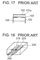
- a conventional piezoelectric transducer to be used as a supersonic probe or the like will be explained with reference to FIGS. 16, 17 and 18.
- FIG. 16 is a perspective view of a conventional piezoelectric transducer and FIG. 17 is a side view of the piezoelectric transducer shown in FIG. 16.
- a piezoelectric transducer 100 consists of an acoustic matching layer 110, a backing material 130, a piezoelectric element 101 and a flexible substrate 120 for applying a voltage to the piezoelectric element.
- the piezoelectric transducer 100 is configured in such a manner that the flexible substrate 120 and the piezoelectric element 101 are attached on the backing material 130 made of a mixture of tungsten powder and an epoxy resin; further, the acoustic matching layer 110 such as a resin is applied or attached on the piezoelectric element 101; and finally, the piezoelectric element 101 is cut into strips by dicing.
- the piezoelectric element 101 is provided with electrodes 102 and 103.
- the electrode 102 is electrically connected to the flexible substrate 120 via an upper surface 101a of the piezoelectric element, so that the electrode 102 is also electrically connected to the side surfaces of the piezoelectric element 101.
- FIG. 18 shows a piezoelectric transducer such that a piezoelectric element is embedded in the resin.
- a conducting wire 240 for applying a voltage is bonded with the conductive adhesive or the like to be embedded in a resin 230.
- a constitution of the general supersonic probe, namely, a general piezoelectric transducer embedded in the resin is as described above.
- the acoustic matching layer made of a resin or the like for efficiently transmitting the supersonic wave to the interior of the living body is provided on the upper surface of the piezoelectric element.
- the optimum thickness of this acoustic matching layer is around 1/4 of a wave length of the supersonic wave to be used. If it becomes thicker, the supersonic wave is attenuated and as a result, detection sensitivity of the pulse wave or the like has been deteriorated. Therefore, in the case of bonding the conducting wire to the piezoelectric element with the conductive adhesive or the like such as the piezoelectric transducer embedded in the resin, it is necessary to make the thickness of the conductive adhesive and the thickness of the conductive wire less than or equal to that of the above mentioned acoustic matching layer, so that it is very difficult to manufacture such a piezoelectric transducer and the thickness of the acoustic matching layer becomes thicker than the optimum thickness. This involves a problem such that the detection sensitivity has been deteriorated.
- a vibration property of the piezoelectric element comes under the influence and if the thick conductive wire is used, unnecessary stress and an unnecessary fixed point are generated in the piezoelectric element and a vibration mode comes under the influence. Further, a resonant frequency is deviated and impedance of the resonant frequency is changed, so that it is not possible to effectively vibrate the piezoelectric element. As a result, this involves a problem such that a desired detection sensitivity cannot be obtained.
- a piezoelectric transducer is constructed in a laminated layer such that at least one sheet of piezoelectric element, to which electrodes are provided at the opposite surfaces, is fixed on a substrate having a plurality of electrodes (hereinafter, referred to as a substrate electrode) and further, an acoustic matching layer is superposed on the above mentioned piezoelectric element, wherein one surface electrode among the surface electrodes, which are respectively provided on the opposite surfaces of the above mentioned piezoelectric element as opposed with each other, is connected to the above mentioned substrate electrodes with conductivity as superimposed with each other and other surface electrode is connected to the above mentioned substrate electrodes with conductivity via the conductive member and further, an end of the above mentioned conductive member to be connected to the surface electrode at the side of the acoustic matching layer of the above mentioned piezoelectric element, namely, the above mentioned other surface electrode has a lateral placing connection structure so that the end of the above mentioned conductive member is capable of being connected there
- the piezoelectric transducer according to the present invention has a constitution comprising a piezoelectric element supporting part such that the piezoelectric element is supported between the above mentioned substrate and the above mentioned piezoelectric element in addition to the above described constitutions.
- the wire connection at the element side by second bonding according to a ball bonding method that is not employed in a semiconductor manufacturing step and the wire connection at element side according to wedge bonding method have been invented and employed as a lateral connection method for a piezoelectric element.
- a piezoelectric transducer characterized in that at least one sheet of piezoelectric element, to which electrodes are provided at the opposite surfaces, is fixed on a substrate having electrodes (hereinafter, referred to as a substrate electrode) ; an acoustic matching layer is placed on the above mentioned piezoelectric element and a supersonic wave is transmitted to an object to be measured by driving the above mentioned piezoelectric element in response to an inputted drive signal so as to receiveareflectedwave from the above mentioned object to be measured; the electrode at the acoustic matching layer side of the above mentioned piezoelectric element (hereinafter, referred to as an upper surface electrode) is electrically connected to the above mentioned substrate electrode via the conductive member; and the thickness of the conductive member that is provided on the above mentioned upper surface electrode is defined as not more than 1/4 of the wave length of the above mentioned supersonic wave.
- this conductive member a film with conductivity and a wire to be provided by wire bonding are available.
- Such a constitution enables to have a desired thickness of the acoustic matching layer without applying a complex patterning to the piezoelectric element. Additionally, it is possible to obtain a desired vibration property because unnecessary stress is not transmitted via the conducting wire, so that loss of the energy becomes smaller and it is possible to transmit and receive the supersonic wave efficiently. Therefore, it is also possible to improve the detection sensitivity.
- a frequency of the supersonic wave to be used is 9.6 MHz and an acoustic velocity of the acoustic matching layer is 2,000 m/s, so that a height of a wire bonding part is defined as around 50 ⁇ m.
- a piezoelectric transducer comprising at least one sheet of piezoelectric element, to which electrodes are provided at the opposite surfaces, a substrate having electrodes (hereinafter, referred to as a substrate electrode) and an acoustic matching layer on the above mentioned piezoelectric element, wherein the electrode at the acoustic matching layer side of the above mentioned piezoelectric element (hereinafter, referred to as an upper surface electrode) is electrically connected to the above mentioned substrate electrode by wire bonding and a supersonic wave is transmitted to an object to be measured by activating the above mentioned piezoelectric element in response to the inputted drive signal so as to receive a reflected wave from the above mentioned object to be measured, a constitution is provided such that a conducting member is connected on the above mentioned upper surface electrode of the above mentioned piezoelectric element so as to trace it thereon by using a second bonding according to a ball bonding method or a wedge bonding method and a manufacturing method thereof is provided. According to such a constitution, it
- the above described substrate is configured in such a manner that it has a piezoelectric element supporting part contacting the above described piezoelectric element on its top surface, the above described lower surface electrode is fixed to the substrate electrode for the lower surface with the conductive adhesive or the like and the above mentioned wire bonding is carried out on the above described upper electrode at the opposite surface of the fixing part that is fixed by the above mentioned adhesive in the above described piezoelectric element.
- the thickness of the above described acoustic matching layer that is provided on the above described piezoelectric element is defined as around 1/4 of the wave length of the above mentioned supersonic wave.
- FIGS. 1 to 10 a first embodiment of a pulse wave detector by the use of a piezoelectric transducer according to the present invention will be explained in detail below.
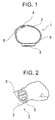
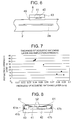
- FIG. 1 is a side view for showing a constitution of the outer shape of the pulse wave detector 1, to which the present invention is applied and FIG. 2 shows a condition that the pulse wave detector 1 shown in FIG. 1 is mounted on a living body 2 (i.e., an arm).
- a living body 2 i.e., an arm
- the pulse wave detector 1 schematically consists of a processing unit 3, a piezoelectric transducer 4, a band 5 and a fastening plate 6.
- the processing unit 3 and the piezoelectric transducer 4 are attached to the band 5 to be fit to the living body 2 (a part encircled by a broken line in FIG. 1) by the band 5 and the fastening plate 6.
- the piezoelectric transducer 4 abuts against the vicinity of a radius artery or an ulnar artery of the living body 2 (not illustrated).
- the processing unit 3 is connected to the piezoelectric transducer 4 by a conducting wire (not illustrated). Then, a driving voltage signal is inputted in the piezoelectric transducer 4 from the processing unit 3 via this conducting wire and a voltage signal that is measured by the piezoelectric transducer 4 is inputted in the processing unit 3.
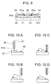
- FIG. 3 is a block diagram for showing the interior constitution of the processing unit 3 and the connection condition of the processing unit 3 and the piezoelectric transducer 4.
- the processing unit 3 schematically consists of an arithmetic processing unit 31, a driving circuit 32 and a display unit 33.
- the arithmetic processing unit 31 carries out various processes with regard to the detection of pulse by carrying out a processing program that is stored in an internal storage area (its illustration is omitted) and displays its processing result in the display unit 33.
- This arithmetic processing unit 31 outputs a specific driving voltage signal from the driving circuit 32 to a piezoelectric element 41 (its details will be described later) of the piezoelectric transducer 4 upon detecting the pulse.
- the arithmetic processing unit 31 compares a frequency of a supersonic wave, which has been transmitted from the piezoelectric element 41 with a frequency of a supersonic wave, which has been received by a piezoelectric element 42 and has been changed due to Doppler effect of blood flow, so that the arithmetic processing unit 31 detects a pulse wave.
- the driving circuit 32 outputs a specific driving voltage signal to the piezoelectric element 41 of the piezoelectric transducer 4 in accordance with the instruction from the arithmetic processing unit 31.
- the display unit 33 consists of a liquid crystal display screen or the like to display the pulse wave detecting result or the like to be inputted from the arithmetic processing unit 31.
- the operations of the processing unit 3 of the pulse wave detector 1 and the piezoelectric transducer 4 will be described below.
- the piezoelectric transducer 4 abuts against the living body 2 (i.e., the vicinity of a radius artery or an ulnar artery of the living body 2).
- the arithmetic processing unit 31 shown in FIG. 3 outputs a specific driving voltage signal from the driving circuit 32 to electrodes of the opposite surfaces of the piezoelectric element 41 (its illustration is omitted) upon detecting the pulse.
- the piezoelectric element 41 generates a supersonic wave as vibrating on the basis of the driving voltage signal that has been inputted in the electrodes on the opposite surfaces of the piezoelectric element 41 and transmits this supersonic wave to the interior of the living body 2 (refer to FIG. 6) via the acoustic matching layer 49.
- the supersonic wave that has been transmitted to the interior of the living body 2 is reflected by a blood flow 2a to be received by the piezoelectric element 42 of the piezoelectric transducer 4.
- the piezoelectric element 42 converts the received supersonic wave into the voltage signal and outputs it from the electrodes on the opposite surfaces to the arithmetic processing unit 31.
- the arithmetic processing unit 31 compares a frequency of a supersonic wave, which has been transmitted from the piezoelectric element 41, with a frequency of a supersonic wave, which has been received by a piezoelectric element 42 and has been changed due to Doppler effect of blood flow, so that the arithmetic processing unit 31 detects a pulse wave of the living body. Then, the arithmetic processing unit 31 displays the detection result of the pulse on the display unit 33. In this manner, the pulse wave detector 1 measures and displays the pulse of the living body.
- the transmission and the reception of the supersonic wave are carried out by different piezoelectric elements, however, it is also possible to switch the transmission and the reception of the supersonic wave with one sheet of piezoelectric element by making time difference upon transmitting and receiving the supersonic wave.
- FIG. 4 is a schematic view for showing a constitution of the piezoelectric transducer 4
- FIG. 5 is a side view of the piezoelectric transducer 4.
- the piezoelectric elements 41 and 42 are provided with an upper surface electrode 52 and a lower surface electrode 53 (they are omitted in FIG. 4). As shown in FIG. 4
- the piezoelectric transducer 4 consists of a substrate 43, the piezoelectric elements 41, the piezoelectric elements 42, a substrate electrode for a lower surface 47a, a substrate electrode for an upper surface 47b and an acoustic matching layer 49, which are provided on the upper surface of the substrate 43.
- the substrate electrodes for the lower surface 47a are electrically connected to lower surface electrodes 53 (refer to FIG. 5) of the lower surface of the piezoelectric elements 41 and 42 (the side of the substrate 43) and the substrate electrodes for the upper surface 47b are electrically connected to upper surface electrodes 52 (refer to FIG. 5) of the upper surface of the piezoelectric elements 41 and 42 (the side of the acoustic matching layer 49) via a wire 61.
- the piezoelectric element is processed into a predetermined size.
- the piezoelectric elements are processed by dicing.
- the piezoelectric element (unillustrated electrodes are placed on the upper and lower surfaces thereof), which is processed into predetermined size, is fixed on the substrate 43.
- the piezoelectric element is processed by dicing.
- the substrate electrodes for the lower surface 47a and the piezoelectric elements 41 and 42 are arranged so that they are superimposed with each other.
- the insulative and conductive adhesives may be used or the piezoelectric elements 41 and 42 may be connected to the substrate electrodes for the lower surface 47a with thermal pressure.
- the lower surface electrodes 53 of the piezoelectric elements 41 and 42 are electrically connected to the substrate electrodes for the lower surface 47a thereby with conductivity.
- the insulative adhesive by applying the insulative adhesive between the piezoelectric elements 41 and 42 and the substrate electrodes for the lower surface 47a and bringing the piezoelectric elements into contact with the substrate electrodes locally by applying pressure on the piezoelectric elements, it becomes possible to connect them with conductivity and fix them with each other.
- the acoustic matching layer 49 is mounted on the substrate 43.
- the acoustic matching layer 49 is made of a hot cured resin, an ultraviolet cured resin or a cold cured resin.
- the acoustic matching layer 49 is coated by spin coating or laminating. In the case of laminating, a film of a certain thickness is used because the acoustic matching layer 49 is needed to be coated evenly with the thickness thereof not more than 0. 1 mm as described later. As shown in FIG.
- the electrodes 47a are electrically connected to the lower surfaces of the piezoelectric elements 41 and 42 and the electrodes 47b are electrically connected to the upper surfaces of the piezoelectric elements 41 and 42, so that it is possible to apply the voltages having different electrical potential to the upper and lower surfaces of the piezoelectric element 41.
- the piezoelectric elements 41 and 42 a PZT of a thickness 0.2 mm (a resonant frequency 9.6 MHz) and an outer shape 0.5 ⁇ 8 mm is used. Additionally, on both sides of the piezoelectric elements 41 and 42, electrodes for applying the voltage are formed through spattering, plating and the like. As the upper surface electrode 52 of the piezoelectric elements 41 and 42, it is preferable to use a gold in view of reliability and strength for wire bonding.
- the gold electrodes are mounted on the upper and lower surfaces of the piezoelectric elements 41 and 42, its manufacturing cost becomes higher, so that it is also possible that the gold electrodes are mounted only on a portion to be applied with the wire bonding by patterning. Additionally, it is possible to use a cheap material such as Al because the wire bonding is not necessary for the lower electrode 53.
- the substrate 43 As the substrate 43 a glass epoxy resin is used.
- the electrodes 47a and 47b are made by plating Cu with gold and its thickness is around 50 ⁇ m.
- a material of the acoustic matching layer 49 an appropriate one is selected in accordance with a material of an object to be inspected and measured by the piezoelectric transducer. However, according to the present embodiment, the material thereof is selected on the basis of a suitability with the living body since the acoustic matching layer 49 is used for detecting the information within the living body (i.e., the human body).
- acoustic impedance of the acoustic matching layer 49 should take a value between the acoustic impedance Zl of the living body and the acoustic impedance Zc of the piezoelectric element.
- the acoustic impedance is a value showing propagation ability of an acoustic wave and its value is changed by Young's modulus and a density thereof.
- the acoustic matching layer 49 an epoxy resin, of which acoustic impedance is about 6 M (N ⁇ sec/m 3 ) and which has ultraviolet hardening, is used.
- the thickness of the acoustic matching layer 49 is also an important element. In the case that the thickness of the acoustic matching layer 49 is improper, as same as the above described acoustic impedance, the supersonic wave is reflected in the acoustic matching layer 49 and further, the supersonic wave is attenuated within the acoustic matching layer 49, so that the supersonic wave is not propagated efficiently.
- the thickness of the acoustic matching layer 49 on the piezoelectric elements 41 and 42 should be about 1/4 of the wave length at the frequency of the supersonic wave to be propagated by the acoustic matching layer 49.
- the frequency of the supersonic wave is 9.6 MHz (normally, the supersonic wave of 2.3 to 10 MHz is used) and the acoustic velocity at the acoustic matching layer 49 is about 2,000 m/s, as the thickness of the acoustic matching layer 49, about 50 ⁇ m is proper.
- the upper surface electrode 52 is sufficiently thinner than the acoustic matching layer, so that normally, it is not necessary to consider the thickness of the upper surface electrode 52 in a normal case.
- this thickness is also considered.
- FIG. 7 shows a measurement result for measuring a thickness of the acoustic matching layer 49 and a reflection strength of the supersonic wave (i.e., a ratio of a signal when the supersonic wave that has been transmitted from the piezoelectric element 41 is detected by the piezoelectric element 42, which is reflected to the brass plate that is set in water and is kept off the piezoelectric transducer 4 by about 4.0 mm as being opposed thereto) to the brass plate set in water.
- a reflection strength of the supersonic wave i.e., a ratio of a signal when the supersonic wave that has been transmitted from the piezoelectric element 41 is detected by the piezoelectric element 42, which is reflected to the brass plate that is set in water and is kept off the piezoelectric transducer 4 by about 4.0 mm as being opposed thereto
- the reflection strength becomes higher when the thickness of the acoustic matching layer 49 is in the range of about 40 to 50 ⁇ m and this reflection strength is not less than twice as that when the thickness of the acoustic matching layer 49 is in the range of 80 to 90 ⁇ m.
- FIG. 8 and FIG. 9 are enlarged views of the piezoelectric transducer according to the present invention.
- FIG. 8 is an explanatory view of a condition such that second bonding according to a ball bonding method is provided to the upper electrodes 52 of thepiezoelectric elements 41 and 42
- FIG. 9 is an explanatory view of a condition such that first bonding according to the ball bonding method is provided to the upper electrodes 52.
- the lower electrode 53 is omitted.
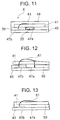
- FIG. 10 is an explanatory view of a general wire bonding step.
- the wire bonding putting the wire 61 (its wire diameter is about 25 ⁇ m) made of a gold or the like through a needle referred to as a capillary 66 as shown in FIG. 10, a ball 61a (its wire diameter is about 100 ⁇ m) is electrically formed at a front end of the wire 61 by discharge (FIG. 10A).
- a chip part 67 such as an IC
- the supersonic wave and melting the ball the ball is electrically connected to the chip part (first bonding) (FIG. 10B).
- the substrate electrode 68 is connected to the wire 61 (second bonding) (FIGS. 10C and 10D).
- the pressure and the supersonic wave energy are stronger in the case of the second bonding, so that, according to a general method of mounting an electronic part, in order to prevent breakage of the chip part, the first bonding is carried out at the side of the chip part and the second bonding is carried out at the side of the substrate electrode.
- a general wire bonding step (ball bonding method) that has been generally carried out in an IC mounting step or the like is as described above.
- a system (a wedge bonding method) is also carried out, whereby a wire is formed only by pressing the capillary as same as the second bonding without forming the ball 61a upon the first bonding.
- a wire diameter of the wire bonding 61 is 25 ⁇ m and the diameter of the ball 61a is in the range of around 50 to 100 ⁇ m.
- the optimum thickness of the acoustic matching layer 49 is about 50 ⁇ m. Therefore, as shown in FIG. 9, if the first bonding according to the ball bonding method is carried out with respect to the upper electrode 52, the wire bonding part becomes higher than the acoustic matching layer 49, so that the wire bonding part protrudes from the acoustic matching layer 49.
- the wire bonding part protrudes from the acoustic matching layer 49, the wire is easily cut and other electric noise is given. If the living body becomes sweaty upon using the present embodiment, the piezoelectric elements 41 and 42 electrically short-circuit, so that this involves a problem such that a desired signal is not obtained.
- the second bonding according to the ball bonding method is carried out with respect to the upper electrode 52, it becomes possible that the wire is connected to the upper electrode 52 as placed in lateral and further, the wire is embedded so that the wire is not exposed from the acoustic matching layer 49. Additionally, according to the second bonding, it is possible to perform the electrical connection at the height as much as the diameter of the wire, so that it is possible to make the wire bonding part thinner than the acoustic matching layer 49. Alternatively, the diameter of the wire to be used for the wire bonding is thin, i.e., 25 ⁇ m, so that the unnecessary stress is hardly generated in the piezoelectric element and it is possible to obtain a desired vibration property.
- the second bonding according to the ball bonding method has been carried out.
- the wedge bonding it is also possible to carry out the wire bonding in the same manner as the ball bonding method. Namely, it is possible to carry out wire bonding as the wire is embedded since it is placed on the upper electrode 52 laterally at the same height as the diameter of the wire. This is accomplished by the first bonding or the second bonding.
- the substrate 43 it is also possible to apply a voltage to the piezoelectric element through the electrode on the rear surface of the substrate 43 by applying a through-hall plating processing or the like to the substrate 43 and providing an electrode on the rear surface of the substrate 43 (i.e., the surface on which the acoustic matching layer 49 is not formed). Further, a detailed part of the present embodiment is not limited to a content of the above described embodiment and it is capable of being altered appropriately without departing from the scope of the subject of the present invention.
- the frequency of the supersonic wave to be used is 9.6 MHz, so that the second bonding is carried out to the upper electrode 52.
- the frequency of the supersonic wave to be used is 1.0 MHz
- the optimum thickness of the acoustic matching layer 49 is not more than 0.45 mm and if the frequency of the supersonic wave to be used is 3.0 MHz, the optimum thickness of the acoustic matching layer 49 is not more than 0.15 mm, so that the wire part is not exposed to the outside of the acoustic matching layer 49 even by the first bonding according to the normal ball bonding method and the first bonding is available.
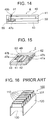
- the substrate 43 there is no need to be a board shape but the substrate 43 may be formed in such a manner that an electrode is provided on a backing material. Furthermore, it is also possible to provide a film made of a metal or the like on the upper electrode 52 in place of the wire bonding. For example, FIG. 15 shows an example such that an electrode 62 of a film type is provided. Although such a constitution may be available as same as above, it is preferable that a soft and small film may be used because the vibration mode of the piezoelectric element is influenced depending on the area and the hardness of the film.
- FIG. 11 is a cross sectional view of the piezoelectric transducer 4 (i.e., an A-A' cross sectional view such that the piezoelectric transducer 4 is cut in a longitudinal direction of the PZT in FIG. 4).
- a piezoelectric element supporting part 59 is provided on the substrate 43.
- an electrode 47b is represented by a broken line.
- the reflection of the supersonic wave arises at a boundary surface between the piezoelectric element and other object.
- This reflected wave causes a noise and it extremely decreases an S/N ratio of the detect signal.
- the electrode to be normally used is made of a copper and a gold, so that the electrode is harder than a layer of the adhesive or the like and the difference of the acoustic impedance thereof becomes larger.
- the reflected wave at the boundary surface between the electrode and the adhesive or at the boundary surface between the electrode and the basic material of the substrate becomes larger. Therefore, as the present embodiment, it is possible to alleviate the above described problem by fixing the piezoelectric elements 41 and 42 on the substrate via the piezoelectric element supporting part 59.
- the piezoelectric elements 41 and 42 are fixed to an electrode 47a via the conductive adhesive 55 and other parts contact the supporting part 59.
- this supporting part 59 has a crena concave portion by keeping out of the electrode 47a so that the piezoelectric elements 41 and 42 are capable of being connected to the electrode 47a with conductivity via conductive adhesive 55.
- resist is used as the supporting part 59. According to such a constitution, the reflection at a boundary surface between the piezoelectric elements 41, 42 and the supporting part 59 becomes smaller, so that it is possible to obtain a desired detection sensitivity.
- FIG. 12 is an explanatory view of the case that the electrode 47b is higher than the supporting part 59.
- the high stress is generated locally in the piezoelectric element 41 and the piezoelectric element 41 is broken.
- the piezoelectric element 41 is broken even if the stress is generated in the piezoelectric element.
- the elasticity of the piezoelectric element is low, so that the piezoelectric element 41 is broken even by a small step.
- the piezoelectric transducer is used as contacting a skin and an object to be measured, so that this involves a problem such that the piezoelectric element is broken when using it. Additionally, as shown in FIG. 12, as shown in FIG. 12, the piezoelectric transducer is used as contacting a skin and an object to be measured, so that this involves a problem such that the piezoelectric element is broken when using it. Additionally, as shown in FIG. 12, as shown in FIG.
- the electrode 47b is formed at a lower position than the supporting part 59 and the wire bonding 61 is carried out on the opposite surface of the fixing part of the electrode 47b and the piezoelectric element 41. Then, even if the second bonding is carried out with respect to the upper electrode 52 of the piezoelectric element, the stress is dispersed and the piezoelectric element is not broken because the piezoelectric element is certainly secured on a bottom surface of this opposite surface and the supporting part 59 is soft. Therefore, the piezoelectric transducer according to the present embodiment is easily manufactured and further, it is possible to decrease the reflection of the supersonic wave, so that it is possible to attain the maintenance and improvement of the detection sensitivity.
- the material of the supporting part 59 has an acoustic impedance (i.e., Young's module and its density) in-between the piezoelectric elements 41 and 42 and the substrate 43.
- the material of the supporting part 59 is preferably soft (at least that of the electrode 47b) so that it absorbs the stress even if the stress is generated in the piezoelectric elements upon the wire bonding or upon using them. According to the present embodiment, in consideration of the patterning, the resist is used.
- FIG. 14 is a cross sectional viewof the piezoelectric transducer 4 (i.e., a cross sectional view cut in a longitudinal direction of the PZT in FIG. 4).
- the acoustic matching layer 49 is needed to be set not more than 1/4 of the wave length of the supersonic wave (in the case of 9.6 MHz, not more than 50 ⁇ m).
- the wire bonding 61 is higher than the acoustic matching layer 49 and in the case that the thickness of the acoustic matching layer 49 should be set lower than the diameter of the wire, as shown in FIG. 14, by making the acoustic matching layer 49 thicker only in the vicinity of the wire bonding 61, the deterioration of the sensitivity is suppressed to the minimum and the wire bonding is capable of being sealed. Further, it is possible to improve durability thereof.
- a manufacturing method of the piezoelectric transducer and a pulse wave detector by the use of the piezoelectric transducer according to the present invention it is possible to drive a piezoelectric element without the need to apply a complex patterning to the piezoelectric element, so that the unnecessary stress is hardly generated in the piezoelectric element and it is possible to make the thickness of acoustic matching layer into a predetermined thickness. Therefore, it is possible to improve the detection sensitivity and to decrease the manufacturing cost thereof. Further, there is an effect such that it is possible to decrease the manufacturing cost of the piezoelectric transducer because the piezoelectric transducer is capable of being manufactured without breaking the piezoelectric element upon the wire bonding.
Landscapes
- Health & Medical Sciences (AREA)
- Life Sciences & Earth Sciences (AREA)
- Cardiology (AREA)
- Engineering & Computer Science (AREA)
- Medical Informatics (AREA)
- Animal Behavior & Ethology (AREA)
- Pathology (AREA)
- Physics & Mathematics (AREA)
- Biomedical Technology (AREA)
- Heart & Thoracic Surgery (AREA)
- Physiology (AREA)
- Molecular Biology (AREA)
- Surgery (AREA)
- Biophysics (AREA)
- General Health & Medical Sciences (AREA)
- Public Health (AREA)
- Veterinary Medicine (AREA)
- Mechanical Engineering (AREA)
- Ultra Sonic Daignosis Equipment (AREA)
- Transducers For Ultrasonic Waves (AREA)
- Investigating Or Analyzing Materials By The Use Of Ultrasonic Waves (AREA)
- Apparatuses For Generation Of Mechanical Vibrations (AREA)
- Measuring Pulse, Heart Rate, Blood Pressure Or Blood Flow (AREA)
Abstract
Description
Claims (18)
- A piezoelectric transducer comprising:wherein the piezoelectric elements are arranged on the substrate, are provided with a first surface electrode (53) to be connected to the first substrate electrode that is arranged on the substrate and a second surface electrode (52) to be connected to the second substrate electrode via a conductive member by connecting other end of the conductive member, of which one end is connected to the second substrate electrode, as opposed to the first surface electrode; an acoustic matching layer (49) for efficiently propagating the supersonic wave on the second surface electrode at the side of the object to be measured is provided; and the other end of the conductive member to be connected to the second surface electrode having a thickness not more than that of the acoustic matching layer is placed laterally embedded in the acoustic matching layer.a substrate (43) having a first substrate electrode (47a) and a second substrate electrode(47b) for forming input and output terminals;one or more piezoelectric element (41, 42) for transmitting a supersonic wave to an object to be measured and receiving a reflected wave from the object to be measured;
- A piezoelectric transducer according to claim 1; wherein
the piezoelectric elements are further provided on the substrate as supporting the piezoelectric elements and simultaneously, the piezoelectric elements are arranged on a piezoelectric element supporting part having a concave portion that is formed as keeping out of the first substrate electrode. - A piezoelectric transducer according to claim 2; wherein
the piezoelectric element supporting part is made of a material, of which mechanical strength is lower than that of the first substrate electrode. - A piezoelectric transducer according to claim 2; wherein
the piezoelectric element supporting part is made of a material, of which mechanical strength is lower than that of adhesive that is formed and solidified for connecting the first substrate electrode to the first surface electrode with conductivity. - A piezoelectric transducer according to any one of claims 1 to 4; wherein
the other end of the conductive member is connected to the second surface electrode in contraposition to the concave portion on the second surface electrode. - A piezoelectric transducer according to any one of claims 1 to 5; wherein
the conductive member comprises a film having conductivity. - A piezoelectric transducer according to any one of claims 1 to 6;
wherein
the conductive member comprises a wire that is provided according to a wire bonding method. - A piezoelectric transducer according to claim 7; characterized in that:the other end of the conductive member is connected to the second surface electrode by second bonding according to a ball bonding method.
- A piezoelectric transducer according to claim 7; wherein
the other end of the conductive member is connected to the second surface electrode according to a wedge bonding method. - A piezoelectric transducer according to any one of the preceding claims; wherein
the thickness of the acoustic matching layer is equivalent to 1/4 of a wave length of the supersonic wave. - A piezoelectric transducer according to any one of the preceding claims; wherein
a material of the first surface electrode that is disposed on the piezoelectric element is different from a material of the second surface electrode that is disposed on the piezoelectric element. - A piezoelectric transducer according to claim 1; wherein
a material of the first surface electrode is a gold. - A pulse wave detector comprising:a piezoelectric transducer according to claim 1;a driving unit for driving the piezoelectric transducer so as to transmit a supersonic wave from the piezoelectric transducer to a living body; anda detecting unit for detecting a pulse wave by a reflected wave from the living body, which is received by the piezoelectric transducer.
- A manufacturing method of a piezoelectric transducer, at least comprising the steps of:fixing a piezoelectric element, on which a first surface electrode and a second surface electrode are mounted as opposed with each other, on a substrate having a first substrate electrode and a second substrate electrode for forming input and output terminals so that the first substrate electrode is connected to the first surface electrode with conductivity; andconnecting the other end of a conductive member, of which one end is connected to the second substrate electrode, to the second surface electrode as placed laterally so that a height of the other end is formed not more than 1/4 of a wave length of a supersonic wave.
- A manufacturing method of a piezoelectric transducer according to claim 14; wherein
the other end of the conductive member is connected to the second surface electrode according to a wire bonding method. - A manufacturing method of a piezoelectric transducer according to claim 14; wherein
the other end of the conductive member is connected to the second surface electrode according to a second bonding method according to a ball bonding method. - A manufacturing method of a piezoelectric transducer according to claim 14; wherein
the other end of the conductive member is connected to the second surface electrode according to a wedge bonding method. - A manufacturing method of a piezoelectric transducer according to claim 14; wherein
the other end of the conductive member is connected to the second surface electrode by using a film conductive member.
Applications Claiming Priority (2)
| Application Number | Priority Date | Filing Date | Title |
|---|---|---|---|
| JP2001352140A JP3908512B2 (en) | 2001-11-16 | 2001-11-16 | Piezoelectric transducer and pulse wave detector |
| JP2001352140 | 2001-11-16 |
Publications (2)
| Publication Number | Publication Date |
|---|---|
| EP1312424A2 true EP1312424A2 (en) | 2003-05-21 |
| EP1312424A3 EP1312424A3 (en) | 2004-04-21 |
Family
ID=19164359
Family Applications (1)
| Application Number | Title | Priority Date | Filing Date |
|---|---|---|---|
| EP20020257892 Withdrawn EP1312424A3 (en) | 2001-11-16 | 2002-11-15 | Piezoelectric transducer, manufacturing method of piezoelectric transducer and pulse wave detector |
Country Status (5)
| Country | Link |
|---|---|
| US (1) | US6924587B2 (en) |
| EP (1) | EP1312424A3 (en) |
| JP (1) | JP3908512B2 (en) |
| CN (1) | CN1419895A (en) |
| CA (1) | CA2411598A1 (en) |
Families Citing this family (30)
| Publication number | Priority date | Publication date | Assignee | Title |
|---|---|---|---|---|
| WO2005036150A1 (en) * | 2003-10-08 | 2005-04-21 | Philips Intellectual Property & Standards Gmbh | Bulk acoustic wave sensor |
| US7815575B2 (en) * | 2005-05-09 | 2010-10-19 | Salutron, Inc. | Ultrasonic monitor with a biocompatible oil based transmission medium |
| US20070016053A1 (en) * | 2005-06-08 | 2007-01-18 | Lo Thomas Y | Ultrasonic monitor with an adhesive member |
| JP2007074697A (en) * | 2005-08-10 | 2007-03-22 | Mitsumi Electric Co Ltd | Ultrasonic device and assembly method thereof |
| US7808156B2 (en) * | 2006-03-02 | 2010-10-05 | Visualsonics Inc. | Ultrasonic matching layer and transducer |
| JP4752715B2 (en) * | 2006-10-13 | 2011-08-17 | 株式会社デンソー | Ultrasonic sensor |
| CN100424485C (en) * | 2006-10-31 | 2008-10-08 | 北京信息工程学院 | Pulsating pressure sensor |
| JP4961224B2 (en) * | 2007-02-02 | 2012-06-27 | 株式会社日立メディコ | Ultrasonic probe |
| JP4412367B2 (en) * | 2007-08-21 | 2010-02-10 | 株式会社デンソー | Ultrasonic sensor |
| US20090088618A1 (en) * | 2007-10-01 | 2009-04-02 | Arneson Michael R | System and Method for Manufacturing a Swallowable Sensor Device |
| JP5104269B2 (en) * | 2007-12-10 | 2012-12-19 | コニカミノルタビジネステクノロジーズ株式会社 | Structural color display |
| CN102048528B (en) * | 2009-11-02 | 2013-06-19 | 广东天琪药业有限公司 | Pulse detector with high interference resistance |
| US8264129B2 (en) * | 2010-07-21 | 2012-09-11 | General Electric Company | Device and system for measuring material thickness |
| CN102288782A (en) * | 2011-07-19 | 2011-12-21 | 江苏物联网研究发展中心 | High-precision ultrasonic transducer |
| JP6089499B2 (en) * | 2012-08-28 | 2017-03-08 | セイコーエプソン株式会社 | Ultrasonic transducer device and probe, electronic device and ultrasonic diagnostic device |
| US9864450B2 (en) * | 2013-06-04 | 2018-01-09 | Nissha Co., Ltd. | Piezoelectric sensor and pressure detection apparatus |
| TWI585375B (en) * | 2014-12-05 | 2017-06-01 | 麥克思股份有限公司 | Ultrasonic sensor and manufacturing method thereof |
| US10265729B2 (en) * | 2015-02-06 | 2019-04-23 | Olympus Scientific Solutions Americas Inc. | Phased array ultrasonic transducers with solderless stack bonding assembly |
| CN205595376U (en) * | 2015-04-30 | 2016-09-21 | 意法半导体股份有限公司 | Piezoelectric sensor |
| US10302595B2 (en) * | 2015-11-06 | 2019-05-28 | Qorvo Us, Inc. | Acoustic resonator devices and fabrication methods providing hermeticity and surface functionalization |
| WO2017187710A1 (en) * | 2016-04-28 | 2017-11-02 | 太陽誘電株式会社 | Vibration waveform sensor and pulse wave detector |
| IL300688B2 (en) | 2016-06-06 | 2024-04-01 | Sofwave Medical Ltd | Ultrasound system and transducer |
| CN106405930B (en) * | 2016-06-27 | 2019-06-11 | 南京中电熊猫液晶显示科技有限公司 | Naked eye three-dimensional display device and its method |
| WO2018061319A1 (en) * | 2016-09-28 | 2018-04-05 | 株式会社村田製作所 | Piezoelectric sound generating component |
| IL280638B1 (en) | 2018-08-02 | 2026-06-01 | Sofwave Medical Ltd | Fat tissue treatment |
| JP7486030B2 (en) * | 2020-01-21 | 2024-05-17 | セイコーエプソン株式会社 | Ultrasonic device and method for manufacturing the same |
| CN115138547A (en) * | 2022-06-30 | 2022-10-04 | 中国工程物理研究院电子工程研究所 | Piezoelectric micromechanical ultrasonic transducer back lining material, preparation method and filling method |
| CN115971020B (en) * | 2023-01-17 | 2024-09-10 | 京东方科技集团股份有限公司 | Ultrasonic transducer and manufacturing method thereof, and ultrasonic transducer system |
| CN116636873A (en) * | 2023-04-21 | 2023-08-25 | 清华大学 | A kind of all-fiber flexible heart sound sensor and preparation method thereof |
| CN118962651B (en) * | 2024-10-14 | 2025-01-21 | 北京海卓同创科技有限公司 | Single beam transducer and control method based on height weighting |
Family Cites Families (10)
| Publication number | Priority date | Publication date | Assignee | Title |
|---|---|---|---|---|
| JPS51130866A (en) * | 1975-05-08 | 1976-11-13 | Seiko Instr & Electronics | Method of mounting electronic timekeeper circuits |
| US4656384A (en) * | 1984-10-25 | 1987-04-07 | Siemens Aktiengesellschaft | Ultrasonic detection sensor in hybrid structure with appertaining electronic circuit |
| JP3318687B2 (en) * | 1993-06-08 | 2002-08-26 | 日本碍子株式会社 | Piezoelectric / electrostrictive film element and method of manufacturing the same |
| EP0651449B1 (en) * | 1993-11-01 | 2002-02-13 | Matsushita Electric Industrial Co., Ltd. | Electronic component and method for producing the same |
| JP3323343B2 (en) * | 1994-04-01 | 2002-09-09 | 日本碍子株式会社 | Sensor element and particle sensor |
| WO1998019349A1 (en) | 1996-10-29 | 1998-05-07 | Motorola Inc. | An ultrasonically mounted piezoelectric device and method of making same |
| JP3913463B2 (en) * | 1999-12-27 | 2007-05-09 | セイコーインスツル株式会社 | Pulse detection device and manufacturing method thereof |
| JP5110751B2 (en) * | 2000-08-24 | 2012-12-26 | セイコーインスツル株式会社 | Ultrasonic diagnostic equipment |
| JP4811972B2 (en) * | 2001-01-22 | 2011-11-09 | セイコーインスツル株式会社 | Ultrasonic diagnostic equipment |
| US6843771B2 (en) * | 2003-01-15 | 2005-01-18 | Salutron, Inc. | Ultrasonic monitor for measuring heart rate and blood flow rate |
-
2001
- 2001-11-16 JP JP2001352140A patent/JP3908512B2/en not_active Expired - Fee Related
-
2002
- 2002-11-08 US US10/290,952 patent/US6924587B2/en not_active Expired - Lifetime
- 2002-11-12 CA CA 2411598 patent/CA2411598A1/en not_active Abandoned
- 2002-11-15 CN CN02150498A patent/CN1419895A/en active Pending
- 2002-11-15 EP EP20020257892 patent/EP1312424A3/en not_active Withdrawn
Also Published As
| Publication number | Publication date |
|---|---|
| JP2003153389A (en) | 2003-05-23 |
| US20030201696A1 (en) | 2003-10-30 |
| US6924587B2 (en) | 2005-08-02 |
| CN1419895A (en) | 2003-05-28 |
| JP3908512B2 (en) | 2007-04-25 |
| EP1312424A3 (en) | 2004-04-21 |
| CA2411598A1 (en) | 2003-05-16 |
Similar Documents
| Publication | Publication Date | Title |
|---|---|---|
| US6924587B2 (en) | Piezoelectric transducer, manufacturing method of piezoelectric transducer and pulse wave detector | |
| US7686765B2 (en) | Pulse detecting device and ultrasound diagnostic apparatus | |
| US7471034B2 (en) | Ultrasound transducer and method of producing the same | |
| US7205701B2 (en) | Passive wireless acoustic wave chemical sensor | |
| US7714482B2 (en) | Ultrasonic sensor | |
| US6744178B2 (en) | Pulse detection device and method of manufacturing the same | |
| EP2227037A1 (en) | Ultrasonic probe, and ultrasonic diagnosis device using the probe | |
| KR100666976B1 (en) | Ultrasonic transducer and its manufacturing method | |
| JP3450430B2 (en) | Ultrasonic transducer | |
| JP4988034B2 (en) | Pulse detection device and ultrasonic diagnostic device | |
| JP2782940B2 (en) | Floating magnetic head device | |
| JP6795986B2 (en) | Ultrasonic probe, ultrasonic diagnostic equipment | |
| KR101572118B1 (en) | Flip-chip bonding device used in contact condition | |
| JP3857518B2 (en) | Pulse detector | |
| JP4738621B2 (en) | Pulse detector | |
| JP4610790B2 (en) | Method for manufacturing piezoelectric transducer | |
| CN214073368U (en) | Miniature ultrasonic blood pressure detection device | |
| JP3857519B2 (en) | Pulse detector | |
| JP3305117B2 (en) | Ultrasonic probe | |
| JPH0552120B2 (en) | ||
| JPH11281555A (en) | Tactile sensor probe | |
| JP2018085636A (en) | Mounting structure, ultrasonic device, ultrasonic probe, ultrasonic device, and electronic device |
Legal Events
| Date | Code | Title | Description |
|---|---|---|---|
| PUAI | Public reference made under article 153(3) epc to a published international application that has entered the european phase |
Free format text: ORIGINAL CODE: 0009012 |
|
| AK | Designated contracting states |
Designated state(s): AT BE BG CH CY CZ DE DK EE ES FI FR GB GR IE IT LI LU MC NL PT SE SK TR |
|
| AX | Request for extension of the european patent |
Extension state: AL LT LV MK RO SI |
|
| PUAL | Search report despatched |
Free format text: ORIGINAL CODE: 0009013 |
|
| AK | Designated contracting states |
Kind code of ref document: A3 Designated state(s): AT BE BG CH CY CZ DE DK EE ES FI FR GB GR IE IT LI LU MC NL PT SE SK TR |
|
| AX | Request for extension of the european patent |
Extension state: AL LT LV MK RO SI |
|
| AKX | Designation fees paid | ||
| REG | Reference to a national code |
Ref country code: DE Ref legal event code: 8566 |
|
| STAA | Information on the status of an ep patent application or granted ep patent |
Free format text: STATUS: THE APPLICATION IS DEEMED TO BE WITHDRAWN |
|
| 18D | Application deemed to be withdrawn |
Effective date: 20041022 |