The present invention relates to an amplification-type
solid image sensor, particularly to a threshold
voltage modulation-type solid image sensor using
a junction gate type field-effect transistor whose
threshold voltage is modulated in accordance with
an incident light as a pixel.
In recent years, a solid image sensor referred to
as an amplification-type has intensively been developed
in which a charge detection circuit is disposed for
each pixel. Above all, a solid image sensor referred
to as a threshold voltage modulation-type has been
noted. In the solid image sensor, a plurality of
pixels including junction-type field-effect transistors
(hereinafter referred to as FET) is arranged in
a matrix. Moreover, when light is incident, a signal
charge is generated in each pixel, and the signal
charges are accumulated in each pixel for a constant
time. In each pixel, a change in a potential or
threshold voltage is generated in a channel region of
FET in each pixel in accordance with an accumulated
amount of signal charges. Furthermore, a plurality of
pixels is successively scanned following a predetermined
order, and image signals are successively read,
for example, by source follower type potential
detection means.
A structure disclosed, for example, in FIG. 14 of
Jpn. Pat. Appln. KOKAI Publication No. 8-78653 has
heretofore been known as the threshold voltage
modulation-type solid image sensor.
FIG. 1 shows a sectional structure of a device for
one pixel of the sensor. An n-type layer 72 is formed
in a p-type substrate 71, and an n+-type drain region
74 and source region 75 are formed in the surface
region of the n-type layer 72 via a P+-type junction
gate 73. Moreover, a MOS type gate electrode 76
for charge reset is formed adjacent to the junction
gate 73.
In this solid image sensor, when light is
incident, a plurality of electron-hole pairs is
generated by photoelectric conversion. The electrons
of the generated electron-hole pairs flow out to the
drain region 74, and the holes are accumulated in the
junction gate 73 to form the signal charge. Since the
junction gate 73 is in a floating state, the potential
of the junction gate 73 changes in accordance with the
accumulated signal charge. Accordingly, the potential
of the n-type layer 72 changes, and this is read out as
the potential or current change of a source.
The solid image sensor shown in FIG. 1 is simple
in the structure, and has a latent advantage suitable
for miniaturization as compared with a charge coupled
device (CCD) type. However, it cannot necessarily be
said that the sensor is used in a broad range. Reasons
are as follows.
That is, the junction gate 73 in which the signal
charge is accumulated includes a P+-type region which
contains p-type impurities with high density, and the
junction gate 73 is potentially brought into the
floating state. Therefore, when the MOS type gate
electrode 76 is turned on, and the signal charge
accumulated in the junction gate 73 is discharged
to the p-type substrate 71, a remaining background
charge exists without being discharged via the junction
gate 73. This background charge amount changes by
a so-called kTC noise in which a heat noise of on
resistance of the MOS type gate electrode 76 is
reflected. Therefore, even after the signal charge is
reset, the background charge remains in the junction
gate 73. A noise charge is superimposed upon the
background charge, and this is read out as noise which
appears on the signal.
Therefore, it is considered that the density of
p-type impurities in the junction gate 73 is lowered in
order to reduce the influence of the background charge.
In this case, however, since the operation becomes
unstable by a charged state of the chip surface,
a capacitance between the junction gate 73 and n-type
layer 72 drops, and a sufficient amount of signal
charges cannot be accumulated, a problem of decrease
of a saturated charge amount occurs. Therefore, there
has heretofore been a demand for solving a problem that
the saturated charge amount drops.
The present invention has been developed in
consideration of the above-described situation, and
an object thereof is to provide a solid image sensor
which has characteristics of a simple structure and
suitability for miniaturization and which can reduce
noises included in a read signal and which has
a sufficient saturated charge amount.
According to one aspect of the present invention,
there is provided a solid image sensor comprises:
This summary of the invention does not necessarily
describe all necessary features so that the invention
may also be a sub-combination of these described
features.
The invention can be more fully understood from
the following detailed description when taken in
conjunction with the accompanying drawings, in which:
Embodiments of the present invention will be
described hereinafter in detail with reference to the
drawings. It is to be noted that corresponding parts
over all the drawings are denoted with the same
reference numerals and redundant description is
avoided.
(First Embodiment)
FIG. 2 is a circuit diagram of a whole solid image
sensor according to a first embodiment of the present
invention. It is to be noted that FIG. 2 shows a two-dimensional
solid image sensor including 3×3, that is,
nine pixels to simplify the description, but another
number of pixels may also be disposed.
In FIG. 2, a plurality of (nine in the present
example) pixels 1 including junction-type FETs are
arranged in a matrix form. Drains and gates of three
pixels 1 in the same row are connected in common to
one of a plurality of (three in the present example)
selection lines 2 to 4. The selection lines 2 to 4 are
connected to a pixel row selection circuit 5 including,
for example, shift registers which output predetermined
pulse signals at a selection time of the pixel row.
Moreover, the sources of three pixels 1 of the
same column are connected in common to one of a
plurality of (three in the present example) signal
lines 6 to 8. Each of the signal lines 6 to 8 is
connected to one end of each of N-channel MOS
transistors 9N to 11N for switch for selecting the
signal line, and other ends of the MOS transistors 9N
to 11N are connected in common. Furthermore, gates of
the MOS transistors 9N to 11N are connected to a pixel
column selection circuit 12 including, for example,
the shift registers which output the predetermined
pulse signals at the selection time of a pixel column.
A current source 13 is connected between a common
connection node of the MOS transistors 9N to 11N
and ground potential . Furthermore, an impedance
conversion circuit 14 for outputting the read signal is
connected to the common connection point of the MOS
transistors 9N to 11N and current source 13.
The solid image sensor shown in FIG. 2 is
integrated in a semiconductor substrate. It is to be
noted that, as not especially shown, a compensation
circuit for offset compensation of each pixel and
a signal processing circuit for performing various
types of signal processing such as A/D conversion of
an output of the impedance conversion circuit 14 are
integrated in the same semiconductor substrate.
In the solid image sensor shown in FIG. 2, when
the light is incident, signal charges are accumulated
in each pixel 1 in accordance with each light amount.
A threshold voltage of each pixel 1 changes in
accordance with an accumulated signal charge amount.
Moreover, when a pulse signal outputted from the pixel
row selection circuit 5 is applied to any one of the
selection lines 2 to 4, the pixel row is selected.
Furthermore, when the pulse signal outputted from
the pixel column selection circuit 12 is applied to any
one of the gates of the MOS transistors 9N to 11N, and
the MOS transistor is turned on, the pixel column is
selected, and thereby one pixel 1 is selected. In this
case, as shown by arrows in FIG. 2, a current path is
formed to extend to the current source 13 from the
selection line (selection line 4 in the present
example) via the selected pixel and further via the
signal line (signal line 7 in the present example) and
the MOS transistor having an on state (MOS transistor
10N in the present example), and a signal is outputted
via the impedance conversion circuit 14 in accordance
with the threshold voltage of the selected pixel.
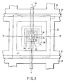
FIG. 3 is a pattern plan view showing the device
structure of one pixel 1 in FIG. 2, and FIGS. 4 and 5
are different sectional views of FIG. 3.
An n-type well region 21 is formed in a surface
region of a p-type semiconductor substrate 20.
A ground potential is supplied to the substrate 20.
Furthermore, in the surface region of the n-type well
region 21, a drain region 22 and a source region 23
including n+-type diffusion regions are formed apart
from each other. Additionally, in the surface region
of the n-type well region 21, an n-type diffusion
region 24 connected to the drain region 22 and extended
in a direction of the source region 23 is formed. The
n-type diffusion region 24 corresponds to the junction
gate of a junction-type FET constituting the pixel 1 in
FIG. 2, and is formed to have a diffusion depth smaller
than that of the drain region 22. Moreover, a p-type
diffusion region 25 for parasitic channel prevention is
formed in the surface region of the n-type well region
21 between the n-type diffusion region 24 and the
source region 23. Furthermore, a p-type embedded
region 26 for signal charge accumulation is formed in
contact with the n-type diffusion region 24 in the well
region 21 under the n-type diffusion region 24.
The source region 23 is disposed substantially
in a middle of a pixel region defined on a one-dot
chain line in FIG. 3. The p-type diffusion region
25 is disposed to surround the source region 23.
Furthermore, the drain region 22 and the n-type
diffusion region 24 connected to the drain region are
disposed to surround the p-type diffusion region 25.
Additionally, the drain region 22 is extended to be
common to the pixels for one row disposed adjacent to
each other in a lateral direction in FIG. 3.
Moreover, the n-type well regions 21 are separated
from each other in a row direction by a device
isolation region 27 extended in a direction parallel to
the extension direction of the drain region 22 as shown
in FIG. 3.
An interlayer insulating film 28 is formed on the
n-type well region 21. Furthermore, a wiring layer 29
corresponding to the signal lines 6 to 8 shown in
FIG. 2 is formed on the interlayer insulating film 28.
Moreover, an opening connected to the surface of
the source region 23 is formed with respect to the
interlayer insulating film 28, and a contact 30 which
connects the source region 23 and wiring layer 29 is
formed in the opening.
It is to be noted that a micro lens for focusing
an incident light is formed for each pixel on the
interlayer insulating film 28, but the lens is not
shown in the drawing to simplify the description.
In the pixel including the above-described section
structure, when the incident light focused by the
on-chip micro lens is emitted, a photodiode including
the n-type diffusion region 24 and p-type embedded
region 26 under the diffusion region performs
photoelectric conversion with a photodiode including
the n-type well region 21 and p-type embedded region
26, and a plurality of electron-hole pairs are
generated. In the generated electron-hole pairs, the
electrons are discharged to the outside via the drain
region 22 without or after drifting in the n-type well
region 21. The holes are accumulated and integrated in
the p-type embedded region 26. The accumulated amount
of the hole corresponds to a product of intensity of
the incident light and integration time. Moreover,
the threshold voltage of each pixel is modulated in
accordance with the accumulated amount of the holes.
Moreover, after the integration of the holes,
each pixel is successively scanned by the pixel row
selection circuit 5 and pixel column selection circuit
12, and the change of the threshold voltage of each
pixel is read as the signal. After reading out the
signal from the pixel, the holes accumulated in each
pixel are discharged to the substrate 20, and a reset
operation is performed.
FIG. 6 is a waveform diagram of major signals in
the solid image sensor shown in FIG. 2. In FIG. 6,
signals S2, S3, S4 are outputted from the pixel row
selection circuit 5, and indicate waveforms of the
pulse signals applied to the selection lines 2 to 4.
Signals S9N, S10N, S11N are outputted from the pixel
column selection circuit 12, and indicate the waveforms
of the pulse signals applied to the gates of the MOS
transistors 9N, 10N, 11N. A signal OUT indicates the
waveform of the signal outputted from the impedance
conversion circuit 14. As shown in FIG. 6, the pulse
signal having a voltage indicating three values VL, VM,
VH is applied to the selection lines 2 to 4. In the
three-valued voltage, VL is lowest, VM is higher than
VL, and VH is higher than VM.
An operation of the solid image sensor of FIG. 2
will next be described with reference to FIG. 6.
A period in which the signals are read out of all
the pixels is referred to as one frame period. In one
frame period, the signals of the selection lines 2 to 4
drop to VL from VH and then drop to VL from VH. In one
frame period, a period in which the signals S2 to S4 of
the selection lines 2 to 4 indicate VL is an accumulation
period of the holes. A period of VM is a readout
period in which the change of the threshold voltage of
each pixel is read out as the signal. Furthermore,
a period of VH is a reset period in which the holes
integrated in each pixel are discharged.
For example, in the period in which the signal S2
of the selection line 2 indicates VM, three pixels 1 in
the row connected to the selection line 2 are selected.
When the signal S9N is set to a high level in this
period, the MOS transistor 9N is turned on, the pixel
column is selected, and the current flows into the
current source 13 via the signal line 6 and the pixels
1 of the selected row and column. Moreover, the signal
indicating the threshold voltage of the selected pixel
is outputted as the signal OUT via the impedance
conversion circuit 14. Furthermore, when the signals
S10N, S11N are successively set to the high level, the
MOS transistors 10N, 11N are successively turned on,
different pixel columns are successively selected,
current flows into the current source 13 via the signal
lines 7, 8 and the corresponding pixels 1 of the
selected column, and the signal indicating the
threshold voltage of the selected pixel is outputted as
the signal OUT via the impedance conversion circuit 14.
The pixel row is changed and successively subjected to
this operation, so that the signals are read out of all
the pixels.
Moreover, after the signals are read out of three
pixels in each pixel row, the signals S2 to S4 of
the selection lines 2 to 4 turn to VH, the holes are
discharged from these three pixels, and the reset
operation is performed to prepare for the next
accumulation of the holes.
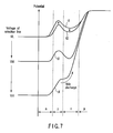
FIG. 7 shows a potential state in a section taken
along a line C-C' of FIG. 5 in timings t1 to t4 in the
waveform diagram of FIG. 6. An accumulation operation
of the holes in each pixel, signal readout operation,
and reset operation will next be described in detail
with reference to the potential diagram of FIG. 7.
In the timing t1 immediately after the start of
the accumulation period immediately after the voltage
value of the pulse signal S4 applied to the selection
line 4 changes to VL, as described above, for the
plurality of electron-hole pairs generated in
accordance with the incident light, the holes are
accumulated and integrated in the p-type embedded
region 26. Accordingly, the potential of the p-type
embedded region 26 drops. Furthermore, accordingly the
potential in the n-type well region 21 under the p-type
embedded region 26 is also modulated and lowered.
In the timing t2 immediately before the end of the
accumulation period, the potential in the n-type well
region 21 is lower than that of the timing t1.
Subsequently, when the readout period is started,
and the pulse signal S4 applied to the selection line 4
changes to VM, the whole potential accordingly drops in
proportion to (VM-VL). Additionally, since the p-type
substrate 20 is fixed at the ground potential, the
potential of the substrate 20 is constant and does not
change. Thereafter, when the signal S9 reaches the
high level, and the MOS transistor 9N in FIG. 2 turns
on, for three pixels of the same column, an electron
current flows via the pixel indicating the lowest
potential of the n-type well region 21 and the constant
current source 13. In this case, while VL is applied
to the other selection lines 2, 3 excluding the
selection line 4, VM is applied to the selection line
4, the potential of the n-type well region 21 of the
pixel connected to the selection line 4 is lowest, and
therefore the electron current flows via the pixel
connected to the selection line 4. The electron
current flowing at this time is shown by arrows in
FIGS. 4 and 5. That is, a source follower is thereby
formed in which the selection line 4 is a power source,
the selected pixel 1 connected to the selection line 4
and signal line 6 is a junction gate type FET, and the
current source 13 is a current source. The potential
is outputted as the signal OUT via the impedance
conversion circuit 14 in accordance with a potential
value of a minimum point of the potential of the n-type
well region 21 of the selected pixel 1. In this case,
since the minimum point of the potential of the n-type
well region 21 is modulated by the integrated value of
the holes generated by the incident light, all the
pixels are scanned by the pixel row selection circuit 5
and pixel column selection circuit 12, the signal is
successively read out of the impedance conversion
circuit 14, and thereby a video signal can be obtained.
Subsequently, in the timing t4 after the readout
period ends and the pulse signal S4 applied to the
selection line 4 changes to VH, the potential of the
p-type embedded region 26 further drops, and the hole
accumulated in the p-type embedded region 26 is thereby
discharged into the substrate 20 via the n-type well
region 21.
As described above, in the solid image sensor of
the first embodiment, each pixel 1 is constituted by
one junction-type FET, and the structure is simple and
suitable for miniaturization as compared with the CCD
type.
Here, the solid image sensor of the first
embodiment will be compared with the conventional
apparatus shown in FIG. 1. In FIG. 1, to accumulate
the charges in the junction gate 73 in the floating
state, an impurity density needs to be set to be
sufficiently high. The reason is that the operation is
prevented from being unstable by charging of a chip
surface. As a result, one portion of the junction gate
73 having the high density forms a neutral region
constantly filled with the electrons or holes, and
the charges are accumulated to neutralize adjacent
acceptors or donors of an opposite conductive type
existing in a depletion layer region in the n-type
layer 72. For example, with reference to FIG. 1,
a surface side of the junction gate 73 containing
the p-type impurity in the high density is constantly
filled with the holes, and the holes as the signals
are accumulated in the depletion layer region formed
between the gate and n-type layer 72. Since the
acceptor in the depletion layer is neutralized in
this state, an electric force line from the donor in
the n-type layer 72 terminated in the acceptor has to
terminate in the acceptor of the substrate 71, and
thereby a potential fluctuation of the P-type junction
gate 73 increases. That is, a capacitance between the
ground potential and the junction gate 73 is remarkably
small. The same is repeated, but it is to be noted
that the n-type layer 72 is completely depleted,
a capacitance is therefore formed between the P-type
junction gate 73 and substrate 71, and a capacitance
to ground can be regarded as extremely small because of
a large distance of the capacitance. Therefore, under
a normal operation voltage, the signal charge amount
accumulated in the floating region is limited, and
the complete depletion of the region is not achieved.
Additionally, when the potential fluctuation is large
with respect to the signal charge, sensitivity can
advantageously be set to be high.
On the other hand, according to the first
embodiment, a sufficient capacitance between the p-type
embedded region 26 and the n-type well region 21,
drain region 22 can be secured , and a sufficient
amount of signal charges (holes) can be accumulated.
Furthermore, the complete depletion of the p-type
embedded region 26 is possible under the usual
operation voltage. In other words, after all, the
first embodiment is different from the conventional
example in the size of the capacitance to the ground in
the accumulation region of the signal charges (holes).
Priority is given to the sensitivity, and a drop of
saturated signal amount causing shot noise deterioration,
and kTC noise by a background charge are
permitted. Alternatively, compromise is made on the
drop of the sensitivity, the generation of the noise is
prevented, and improvement of a general S/N ratio is
aimed. The scope by the first embodiment lies in the
latter way of thinking.
Furthermore, for the solid image sensor using a
polysilicon gate electrode such as the charge coupling
device type or MOS transistor, since a photoelectric
conversion region is disposed under the polysilicon
gate electrode, influence of absorption of the light
by the polysilicon gate electrode is exerted, and
sensitivity to blue drops.
However, in the solid image sensor of the first
embodiment, the junction gate FET is used in which the
polysilicon gate electrode is not used. Therefore, an
effect that the sensitivity to blue can be prevented
from dropping can also be obtained.
Furthermore, since the photodiode including the
p-type embedded region 26 under the n-type diffusion
region 24 and n-type well region 21 to perform the
photoelectric conversion, and the p-type embedded
region 26 for accumulating the charges are integrated
in a vertical direction of the substrate, the size of
the pixel can effectively be miniaturized as compared
with the photodiode and region formed separately from
each other.
(Second Embodiment)
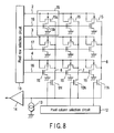
FIG. 8 is a whole circuit diagram of the solid
image sensor according to a second embodiment of the
present invention. It is to be noted that the two-dimensional
solid image sensor including 3×3, that is,
nine pixels is illustrated also in this embodiment in
order to simplify the description, but more pixels may
also be disposed.
The solid image sensor shown in FIG. 8 is slightly
different from that of FIG. 2 in the constitutions of
the pixel and pixel row selection circuit, the other
constitution is similar to that of FIG. 2, and
therefore only respects different from FIG. 2 will be
described.
In FIG. 8, each pixel 15 includes a constitution
in which a MOS type gate portion 15b for discharging
the accumulated charges of the gate of a junction-type
FET portion 15a to a ground potential is added to the
junction-type FET portion 15a including the source,
drain, and gate.
The drains and gates of three pixels 15 of the
same row are connected in common to one corresponding
line of a plurality of (three in the present example)
selection lines 2 to 4 for pixel row selection.
Moreover, the gates of the MOS type gate portions 15b
of three pixels 15 of the same row are connected in
common to one corresponding line of a plurality of
(three in the present example) selection lines 16 to 18
for electric discharge of the pixel row.
The selection lines 2 to 4 and 16 to 18 are
connected to a pixel row selection circuit 19
including, for example, the shift registers which
output the predetermined pulse signals at the selection
time of the pixel row.
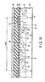
FIG. 9 is a pattern plan view showing the device
structure of one pixel 15 in FIG. 8, and FIG. 10 is
a sectional view of FIG. 8. It is to be noted that for
a section crossing at right angles to the section of
FIG. 10, the gate insulating film of the MOS type gate
portion 15b is simply added to FIG. 4, the other
constitution is similar to that of FIG. 4, and the
section is therefore omitted from the drawing.
In the first embodiment, the drain region 22 is
formed to surround the whole periphery of the p-type
diffusion region 25. On the other hand, in the second
embodiment, the drain region 22 is formed to surround
three sides of the p-type diffusion region 25 whose
plane shape is substantially rectangular. Moreover,
a MOS type gate electrode 31 is formed so as to contact
the p-type embedded region 26 in a portion in which
the drain region 22 is not formed. The MOS type gate
electrode 31 corresponds to the gate of the MOS type
gate portion 15b in FIG. 8, and further corresponds
to any one of the selection lines 16 to 18 in FIG. 8.
As shown in FIG. 10, the MOS type gate electrode 31 is
formed on the substrate 20 via a gate insulating film
32. It is to be noted that the p-type substrate 20
is extended to the surface under the MOS type gate
electrode 31. Moreover, similarly as the first
embodiment, the micro lens is formed for each pixel on
the interlayer insulating film 28, and is omitted from
the drawing so as to simplify the description.
In the solid image sensor, when each pixel is
irradiated with the incident light focused by the micro
lens, the photodiode including the n-type diffusion
region 24 and p-type embedded region 26 under the
diffusion region performs the photoelectric conversion
with the photodiode including the n-type well region 21
and p-type embedded region 26 to generate the plurality
of electron-hole pairs. In the generated electron-hole
pairs, the electrons are discharged to the outside via
the drain region 22 without or after drifting in the
n-type well region 21. The holes are accumulated
and integrated in the p-type embedded region 26.
The accumulated amount of the holes corresponds to
the product of the intensity of incident light and
the integration time. Moreover, the threshold voltage
of each pixel is modulated in accordance with the
accumulated amount of the holes.
Moreover, after the integration of the holes,
each pixel is successively scanned by the pixel row
selection circuit 19 and pixel column selection circuit
12, and the change of the threshold voltage of each
pixel is read as the signal. After reading out the
signal from the pixel, the holes accumulated in each
pixel is discharged to the substrate 20 via the MOS
type gate portion 15b controlled by the pixel row
selection circuit 19, and the reset operation is
performed.
FIG. 11 is a waveform diagram of the major signals
in the solid image sensor shown in FIG. 8. In FIG. 11,
the signals S2, S3, S4 are outputted from the pixel row
selection circuit 19, and indicate the waveforms of the
pulse signals applied to the selection lines 2 to 4 for
row selection. Signals S16, S17, S18 are outputted
from the pixel row selection circuit 19, and indicate
the waveforms of the pulse signals applied to the
selection lines 16 to 18 for electric discharge.
The signals S9N, S10N, S11N are outputted from the
pixel column selection circuit 12, and indicate the
waveforms of the pulse signals applied to the gates of
the MOS transistors 9N, 10N, 11N. The signal OUT
indicates the waveform of the signal outputted via the
impedance conversion circuit 14.
An operation of the solid image sensor of FIG. 8
will next be described with reference to FIG. 11.
As shown in FIG. 11, the pulse signals S2 to S4
having the voltages indicating two values VL and VH are
applied to the selection lines 2 to 4, and the pulse
signals S16 to S18 having the voltages indicating two
values VL and VH are also similarly applied to the
selection lines 16 to 18. In the voltage indicating
two values, VL is lower than VH.
The period in which the signals are read out of
all the pixels is referred to as one frame period.
In one frame period, the signals S2 to S4 of the
selection lines 2 to 4 drop to VL from VH and then drop
to VL from VH. In one frame period, the period in
which the signals S2 to S4 of the selection lines 2 to
4 indicate VL is the accumulation period of the holes.
The readout period in which the change of the threshold
voltage of each pixel is read out as the signal is
a period in which the signals S2 to S4 of the selection
lines 2 to 4 indicate VH and the signals S16 to S18 of
the selection lines 16 to 18 indicate VH. In the reset
period in which the holes accumulated in each pixel 15
are discharged, the signals S2 to S4 of the selection
lines 2 to 4 indicate VH and the signals S16 to S18 of
the selection lines 16 to 18 indicate VL. The reset
period is a period T in FIG. 11.
For example, in the period in which the signal S2
of the selection line 2 indicates the high level (VH),
three pixels 15 in the same row connected to the
selection line 2 are selected. When the signal S9N is
set to the high level (VM) in this period, the MOS
transistor 9N is turned on, the pixel column is
selected, the electron current flows into the current
source 13 via the signal line 6 and the pixels 15 of
the selected row and column, and the signal indicating
the threshold voltage of the selected pixel is
outputted as the signal OUT via the impedance
conversion circuit 14. Furthermore, when the signals
S10N, S11N are successively set to the high level, the
MOS transistors 10N, 11N are successively turned on,
different pixel columns are selected, electron current
flows into the current source 13 via the signal lines
7, 8 and the corresponding pixels 15 of the selected
column, and the signal indicating the threshold voltage
of the selected pixel is successively outputted as the
signal OUT via the impedance conversion circuit 14.
The pixel row is changed and successively subjected to
this operation, so that the signals are read out of all
the pixels.
Moreover, immediately before the end of the signal
readout period from three pixels in each pixel row,
the signals S16 to S18 of the selection lines 16 to 18
indicate a low level (VL). Thereby, the depletion
layer of the surface of the p-type substrate 20 under
the MOS type gate electrode 31 constituting the MOS
type gate portion 15b of each pixel in FIG. 10
disappears, and a uniform potential is obtained. As a
result, the holes accumulated in the p-type embedded
region 26 flows into the substrate 20 via the portion
under the MOS type gate electrode 31, and the reset
operation is performed.
It is to be noted that the reset operation is
performed, when the signals S2 to S4 of the signal
lines 2 to 4 indicate VM and the signals S16 to S18 of
the selection lines 16 to 18 indicate VL. Therefore,
the signals S16 to S18 of the signal lines 16 to 18
are raised to VM, before the signals S2 to S4 of the
selection lines 2 to 4 reach VM and the readout period
is started. Thereby, the reset operation is prevented
from being performed.
FIG. 12 shows the potential state in the section
taken along a line D-D' of FIG. 10 in the timings t1 to
t4 in the waveform diagram of FIG. 11.
The accumulation operation of the holes in each
pixel, signal readout operation, and reset operation
will next be described in detail with reference to the
potential diagram of FIG. 12.
In the timing t1 immediately after the start of
the accumulation period immediately after the pulse
signal S4 applied to the selection line 4 changes to
VL, as described above, for the electron-hole pairs
generated in accordance with the incident light, the
holes are accumulated and integrated in the p-type
embedded region 26. Accordingly, the potential of
the p-type embedded region 26 drops. Furthermore,
accordingly the potential in the n-type well region 21
under the p-type embedded region 26 is also modulated
and lowered. In the timing t2 immediately before the
end of the accumulation period, the potential in the
n-type well region 21 is lower than that of the
timing t1.
Subsequently, when the readout period is started,
and the pulse signal S4 applied to the selection line 4
changes to VH, the whole potential accordingly drops in
proportion to (VH-VL). Additionally, since the p-type
substrate 20 is fixed at the ground potential, the
potential of the substrate 20 is constant and does not
change. Thereafter, when the signal S9 reaches the
high level (VH), and the MOS transistor 9N in FIG. 8
turns on, for three pixels of the same column, the
electron current flows via the pixel indicating the
lowest potential of the n-type well region 21 and the
constant current source 13. In this case, while VL is
applied to the other selection lines 2, 3 excluding the
selection line 4, VH is applied to the selection line
4, the potential of the n-type well region 21 of the
pixel connected to the selection line 4 is lowest, and
therefore the electron current flows via the pixel
connected to the selection line 4. A path of the
current flowing at this time is shown by an arrow a in
FIG. 10. That is, the source follower is thereby
formed in which the selection line 4 is the power
source, the selected pixel 15 connected to the
selection line 4 and signal line 6 is the junction gate
type FET, and the current source 13 is the current
source. The potential is outputted as the signal OUT
via the impedance conversion circuit 14 in accordance
with the potential value of the minimum point of the
potential of the n-type well region 21 of the selected
pixel 15. In this case, since the minimum point of
the potential of the n-type well region 21 is modulated
by the integrated value of the holes generated by the
incident light, all the pixels are scanned by the pixel
row selection circuit 19 and pixel column selection
circuit 12, the signal is successively read out of the
impedance conversion circuit 14, and thereby the video
signal can be obtained.
Subsequently, in a state in which the pulse signal
S4 applied to the selection line 4 indicates VH, and in
the timing t4 after the pulse signal S18 applied to the
selection line 18 changes to VL from VH, the depletion
layer of the surface of the p-type substrate 20 under
the MOS type gate electrode 31 in FIG. 10 disappears,
and the holes accumulated in the p-type embedded region
26 flows into the substrate 20 along a path of a shown
arrow b. Thereby, the potential of the p-type embedded
region 26 increases, the potential of the n-type well
region 21 accordingly increases, and the reset
operation is performed.
As described above, also in the solid image sensor
of the second embodiment, each pixel is substantially
constituted by one junction-type FET, and the structure
is simple and suitable for miniaturization as compared
with the CCD type.
Furthermore, similarly as the first embodiment,
the capacitance between the p-type embedded region 26
and the n-type well region 21, drain region 22 can
sufficiently be secured , and the sufficient amount
of signal charges (holes) can be accumulated.
Additionally, the complete depletion of the p-type
embedded region 26 is possible under the usual
operation voltage. As a result, the noise is prevented
from being generated and the improvement of the general
SN ratio can be achieved.
Furthermore, similarly as the first embodiment,
the junction-type gate FET is used in which the
polysilicon gate electrode is not used. Therefore, the
effect that the sensitivity to blue can be prevented
from dropping is obtained.
Moreover, since the photodiode including the
p-type embedded region 26 under the n-type diffusion
region 24 and n-type well region 21 to perform the
photoelectric conversion, and the p-type embedded
region 26 for accumulating the charges are integrated
in the vertical direction of the substrate, the size of
the pixel can effectively be miniaturized as compared
with the photodiode and region formed separately from
each other.
In the second embodiment, the signals each having
two voltage values can be used as the pulse signals S2
and S3 and S16 to S18 for controlling the readout and
discharge of the signals, it is therefore unnecessary
to generate a pulse signal which has a large voltage
amplitude, and an effect is obtained that a circuit
scale of the pixel row selection circuit 19 can be
reduced as compared with the pixel row selection
circuit 5 of the embodiment of FIG. 2.
The operation of the solid image sensor of the
second embodiment will next be further studied.
FIG. 13 shows the potential state in the
section taken along lines E-E' and F-F' of FIG. 10.
Concretely, the selection lines 4 and 18 in FIG. 8, and
the potential states of the pixels connected to both
the selection lines in the respective timings t1 to t4
in FIG. 11 are shown.
In FIG. 13, A to D show the potential states in
an E-E' section, A shows the state of the timing t1
immediately after the integration start, B shows
the state of the timing t2 immediately before the
integration end, C shows the state of the timing t3
immediately after the readout start, and D shows the
state of the timing t4 in the signal charge discharge
period. Similarly, E and F show the potential states
in the E-E' section, E shows the state of the timing t1
immediately after the integration start, F shows
the state of the timing t2 immediately before the
integration end, F shows the state of the timing t3
immediately after the readout start, and E shows the
state of the timing t4 in the signal charge discharge
period.
Furthermore, in FIG. 13, 1 to 6 have potentials:
1 has the potential which determines a maximum
amount of accumulatable holes; 2 shows the potential
indicating an allowance for preventing the integrated
holes from overflowing at an integration end time; 3
shows the potential indicating an allowance for
preventing the integrated holes from overflowing at
a readout start time; 4 shows the potential
corresponding to an allowable value of a rise of the
potential by the source follower for electron current
detection of the pixel in which the holes are not
accumulated at the readout time; 5 shows the potential
corresponding to the allowable value of the rise of
the potential by a source follower current for the
current detection of the pixel in which the holes are
accumulated at the readout time; and 6 shows the
potential corresponding to a drain voltage allowance
for setting the source follower operation for the
current detection of the pixel to be normal at the
readout time. It is to be noted that the direction
of the arrow of each potential indicates positive
polarity.
For the normal operation, each potential needs to
be in the detection shown in FIG. 13. In other words,
all the potentials need to have positive polarity.
Moreover, for 4 and 5, when 4 has the positive
polarity, 5 also has the positive polarity.
Furthermore, when the value of 4 is extremely small,
the source follower current cannot have a sufficient
value, and operation speed is limited. Therefore,
design consideration is necessary.
One-dimensional consideration has been described.
In actual, since the potential two-dimensionally
spreads, further consideration is necessary.
FIGS. 14 and 15 two-dimensionally show the
potential state in the section in the vicinity of the
MOS type gate electrode 31 in FIG. 10. It is to be
noted that FIG. 14 shows the state in the timing t3
immediately after the readout start, and FIG. 15 shows
the state in the timing t4 at the electric discharge
time. Moreover, each voltage shown in the drawing
indicates the potential. When the voltage value
increases, the potential deepens. This follows
a conventional notation of the solid image sensor.
As shown in FIG. 14, immediately after the readout
start (t = t3), a maximum point R of the potential is
positioned in the n-type well region 21, and a minimum
point Q is positioned in the p-type embedded region 26.
That is, the maximum and minimum points of the
potential are separated from each other. Moreover,
potential differences of the maximum point R and
minimum point Q of the potential from saddle points
P are operation allowances.
At the signal charge discharge time (t = t4),
as shown by an arrow in FIG. 15, the potential
successively drops toward the substrate from the p-type
embedded region 26, and the charge accumulated in the
p-type embedded region 26 is discharged to the
substrate.
(Third Embodiment)
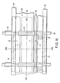
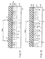
FIG. 16 is a pattern plan view showing the device
structure of the pixel 15 which includes a constitution
different from that of FIG. 9, and FIGS. 17 and 18 are
different sectional views in FIG. 16.
In the pixel shown in FIG. 9, the p-type diffusion
region 25 is formed to surround the source region 23
in a middle, the p-type embedded region 26 is further
formed to surround the p-type diffusion region 25, and
the drain region 22 is formed to surround three sides
of the p-type diffusion region 25. This case has been
described.
On the other hand, according to the third
embodiment, the source region 23, p-type diffusion
region 25, p-type embedded region 26, and drain region
22 are extended in parallel with one another in the
same direction.
Moreover, the MOS type gate electrode 31 includes
a portion extended/formed in parallel with the source
region 23, p-type diffusion region 25, p-type embedded
region 26, and drain region 22 on the device isolation
region 27, and a portion positioned under the wiring
layer 29 and extended in parallel with the wiring layer
29. Furthermore, the portion of the MOS type gate
electrode 31 positioned under the wiring layer 29 is
interrupted midway in the drain region 22 so that the
portions are separated from each other between the
pixels disposed adjacent to each other in a vertical
direction in the drawing.
It is to be noted that the p-type diffusion region
25 is extended/formed over a plurality of pixels so
that the region is common to the plurality of pixels,
but may also be separated for each pixel.
In this constitution, the potential state in each
of the timings t1 to t4 in the section taken along
lines H-H' and I-I' in FIG. 17 is similar to that shown
in FIG. 13, the potential state in each of the timings
t1 to t4 in the section taken along line J-J' in
FIG. 18 is similar to that shown in FIG. 11, and the
description thereof is omitted.
According to the third embodiment, when the
electron current is passed through the source region 23
from the drain region 22 in accordance with the charge
(hole) accumulated in the p-type embedded region 26,
the current flows in a direction XVIII-XVIII in FIG. 16
(vertical direction of FIG. 16). On the other hand,
when the charge accumulated in the p-type embedded
region 26 is discharged, the charge (hole) is
discharged in a direction XVII-XVII in FIG. 16
(horizontal direction of FIG. 16).
According to the third embodiment, effects similar
to those of the first and second embodiments are
obtained, and additionally the following effect is
obtained. That is, the source region 23, p-type
diffusion region 25, p-type embedded region 26, and
drain region 22 are extended in parallel with one
another in the same direction, and the source region 23
is disposed in a peripheral portion rather than in the
middle of the pixel. Therefore, the contact 30 for
connecting the wiring layer 29 to the source region 23
can be disposed in the peripheral portion, not in
the middle of the pixel, a photodiode region can be
disposed in the middle of the pixel, and an improvement
effect of a focus ration by the on-chip micro lens can
be obtained.
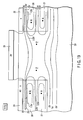
FIG. 19 two-dimensionally shows the potential
state of the section in the vicinity of the MOS type
gate electrode 31 in the timing t3 immediately after
the readout start of the pixel shown in FIG. 16.
Similarly as FIGS. 14, 15, the voltage shown in FIG. 19
indicates the potential.
As shown in FIG. 19, the third embodiment is
similar to the second embodiment in that the maximum
point R of the potential is positioned in the n-type
well region 21 and the minimum point Q is positioned in
the p-type embedded region 26. Furthermore, the third
embodiment is different from the embodiment of FIG. 14
in that the maximum and minimum points are generated on
opposite sides of the MOS type gate electrode 31 in
a symmetric state.
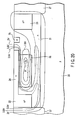
FIG. 20 schematically shows an effect of parasitic
channel prevention by the formed p-type diffusion
region 25 in the first to third embodiments, and shows
the potential state in the section taken along line
XVII-XVII in FIG. 16. Also in this case, the voltage
shown in the drawing indicates the potential.
As shown, when the p-type diffusion region 25 is
formed, the generation of the channel is suppressed in
the surface, and the electron current flows in a path
shown by a broken line in the drawing between the drain
region 22 and source region 23. That is, the current
is prevented from flowing between the drain region 22
and source region 23 through the surface region of the
n-type well region 21.
(First Modification Example of Third Embodiment)
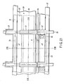
FIG. 21 is a pattern plan view showing the device
structure of the pixel 15 which includes a constitution
different from that of FIG. 16. In the pixel shown in
FIG. 16, the device isolation region 27 is extended in
a direction parallel to an extension direction of the
source region 23. On the other hand, for the pixel 15
according to the modification example, one portion of
the device isolation region 27 is extended, and one
portion of the device isolation region 27 is positioned
between the source regions 23 of the pixels 15 disposed
adjacent to each other in the lateral direction in
FIG. 21.
It is to be noted that a section taken along
a line XVII-XVII and a section taken along a line
XVIII-XVIII in FIG. 21 are similar to those of FIGS. 17
and 18, and are therefore omitted from the drawings.
According to the first modification example,
an effect similar to that of the third embodiment is
obtained. Additionally, since one portion of the
device isolation region 27 is formed between the source
regions 23 of the pixels disposed adjacent to each
other in the lateral direction in FIG. 21, isolation
capability of the pixels can effectively and easily be
enhanced as compared with the isolation by the MOS type
gate electrode 31. That is, with the isolation by the
MOS type gate electrode 31, the value of the voltage
applied to the MOS type gate electrode 31 needs to be
adjusted in accordance with impurity density of the
substrate 20, but with the isolation by the device
isolation region 27, such adjustment is not required
at all.
(Second Modification Example of Third Embodiment)
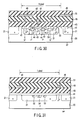
FIG. 22 is a sectional view showing the device
structure in the vicinity of the MOS type gate
electrode 31 of the pixel which includes a constitution
different from that of FIG. 16. For the pixel
according to the modification example, in the p-type
substrate 20 under the MOS type gate electrode 31,
an embedded region 33 which has a polarity reverse to
the p-type, that is, n-type is formed adjacent to the
p-type embedded regions 26, and an embedded region 34
which has a polarity reverse to the n-type, that is,
p-type is formed adjacent to the n-type well regions
21. It is to be noted that the n-type embedded region
33 contacts the p-type embedded region 34 in the
vertical direction.
When the n-type embedded region 33 is formed
adjacent to the embedded region 26 and the p-type
embedded region 34 is formed adjacent to the n-type
well region 21 in this manner, desired accumulation and
discharge operations of the charges can be achieved
without so precisely controlling the dosage of
impurities in the p-type embedded region 26 and n-type
well region 21.
(Fourth Embodiment)
FIG. 23 is a whole circuit diagram of the solid
image sensor according to a fourth embodiment of
the present invention.
In the solid image sensor of FIG. 2, the drains
of the pixels 1 are connected to the corresponding
selection lines 2 to 4, but in the fourth embodiment
the drains of all the pixels 1 are connected to the
ground potential.
Moreover, as switches, connected to the signal
lines 6 to 8, for selecting the signal lines, P-channel
MOS transistors 9P to 11P are used in the fourth
embodiment. Furthermore, the current source 13 is
connected between the common connection point of the
MOS transistors 9P to 11P and a positive potential such
as a power potential Vcc, and the current source 13
supplies the hole and passes the current to each
pixel 1.
In the solid image sensor shown in FIG. 23,
similarly as FIG. 2, a plurality of pixels are
integrated in the semiconductor substrate. It is to be
noted that as not especially shown, the compensation
circuit for offset compensation of each pixel and the
signal processing circuit for performing various types
of signal processing such as A/D conversion of the
output of the impedance conversion circuit 14 are
integrated in the same semiconductor substrate.
In the solid image sensor shown in FIG. 23,
when the light is incident, the signal charges are
accumulated in each pixel in accordance with each light
amount, and the threshold voltage of each pixel 1
changes in accordance with the accumulated signal
charge amount. Moreover, when the pulse signal
outputted from the pixel row selection circuit 5 is
applied to any one of the selection lines 2 to 4, the
pixel row is selected. Furthermore, when the pulse
signal outputted from the pixel column selection
circuit 12 is applied to any one of the gates of the
MOS transistors 9P to 11P, and the MOS transistor is
turned on, the pixel column is selected, and thereby
one pixel 1 is selected. In this case, as shown by
arrows in FIG. 23, the current path is formed to extend
to the ground potential via the power source Vcc,
current source 13, MOS transistor having the on state
(MOS transistor 10P in the present example), signal
line (signal line 7 in the present example), and
selected pixel, and the signal is outputted via the
impedance conversion circuit 14 in accordance with
the threshold voltage of the selected pixel.
FIG. 24 is a pattern plan view showing the device
structure of one pixel 1 in FIG. 23, and FIGS. 25 and
26 are different sectional views.
The n-type well region 21 whose separated plane
shape for each pixel is rectangular is formed in the
surface region of the p-type semiconductor substrate
20. The ground potential is supplied to the p-type
substrate 20. Furthermore, in the surface region of
the n-type well region 21, a drain region 41 and source
region 42 including P+-type diffusion regions are
formed apart from each other. The drain region 41 is
disposed over the n-type well region 21 of the adjacent
pixel, and the source region 42 is disposed substantially
in the middle of the pixel region defined by
a one-dot chain line in FIG. 24. Additionally, in
the surface region of the n-type well region 21 between
the drain region 41 and source region 42, an n+-type
diffusion region 43 is formed. Moreover, in the n-type
well region 21 under the n+-type diffusion region 43,
a p-type diffusion region 44 is formed to contact the
n+-type diffusion region 43 in the vertical direction.
The n+-type diffusion region 43 and p-type
diffusion region 44 are disposed to surround the source
region 42. Furthermore, the drain region 41 is
disposed to surround the n+-type diffusion region 43
and p-type diffusion region 44. Additionally, the
drain region 41 is extended to be common to the pixels
for one row disposed adjacent to each other in the
lateral direction in FIG. 24.
A first interlayer insulating film 45 is formed on
the n-type well region 21. Furthermore, a wiring layer
46 corresponding to the signal lines 6 to 8 shown in
FIG. 23 is formed on the first interlayer insulating
film 45. Moreover, an opening connected to the surface
of the source region 42 is formed with respect to the
first interlayer insulating film 45, and a contact 47
which connects the source region 42 and wiring layer 46
is formed in the opening. Furthermore, a second
interlayer insulating film 48 is formed on the wiring
layer 46, and a wiring layer 49 is formed on the second
interlayer insulating film 48. Moreover, an opening
connected to the surface of the n+-type diffusion
region 43 is formed with respect to the second
interlayer insulating film 48 and first interlayer
insulating film 45, and a contact 50 which connects
the n+-type diffusion region 43 and wiring layer 49 is
formed in the opening. Furthermore, a third interlayer
insulating film 51 is formed on the wiring layer 49.
As shown in FIG. 24, the wiring layer 46 is
extended along one side of each pixel in the vertical
direction of FIG. 24. Moreover, one portion of the
wiring layer 46 is extended to the position of the
source region 42 positioned in the middle of the pixel,
and electrically connected to the source region 42 via
the contact 47. Furthermore, the wiring layer 49 is
extended along one side of each pixel different from
the above-described side in the horizontal direction of
FIG. 24. Additionally, one portion of the wiring layer
49 is extended to the position of the n+-type diffusion
region 43 positioned in the middle portion of the
pixel, and electrically connected to the n+-type
diffusion region 43 via a plurality of (e.g., four in
the present example) contacts 50.
It is to be noted that a micro lens for focusing
the incident light is formed for each pixel on the
third interlayer insulating film 51, but the lens is
not shown in the drawing to simplify the description.
In the pixel including the above-described section
structure, when the incident light focused by the
on-chip micro lens is emitted, the photodiode including
the p-type diffusion region 44 and n-type well region
21 under the diffusion region performs photoelectric
conversion with the photodiode including the n-type
well region 21 and p-type substrate 20, and a
photodiode including the drain region 41 and the n-type
well region 21 under the drain region, and the
plurality of electron-hole pairs are generated. In the
generated electron-hole pairs, the holes flow to the
outside via the drain region 41. On the other hand,
the electrons are accumulated and integrated in the
n-type well region 21 under the p-type diffusion
region 44. The accumulated amount of the electrons
corresponds to the product of the intensity of the
incident light and the integration time. Moreover,
the threshold voltage of each pixel is modulated in
accordance with the accumulated amount of the electron.
Moreover, after the integration of the charge
(electrons), each pixel is successively scanned by
the pixel row selection circuit 5 and pixel column
selection circuit 12, and the change of the threshold
voltage of each pixel is read out as the signal. After
reading out the signal from the pixel, the electron
accumulated in each pixel is discharged to the n+-type
diffusion region 43, and the reset operation is
performed.
FIG. 27 is a waveform diagram of the major
signals in the solid image sensor shown in FIG. 23.
In FIG. 27, the signals S2, S3, S4 are outputted from
the pixel row selection circuit 5, and indicate the
waveforms of the pulse signals applied to the gate of
each pixel via the selection lines 2 to 4. Signals
S9P, S10P, S11P are outputted from the pixel column
selection circuit 12, and indicate the waveforms of
the pulse signals applied to the gates of the MOS
transistors 9P, 10P, 11P. The signal OUT indicates the
waveform of the signal outputted from the impedance
conversion circuit 14.
As shown in FIG. 27, the pulse signals S2 to S4
having the voltage indicating three values VL, VM, and
VH are applied to the selection lines 2 to 4. In the
three-valued voltage, VL is lowest, VM is higher than
VL, and VH is higher than VM.
An operation of the solid image sensor of FIG. 23
will next be described with reference to FIG. 27.
The period in which the signals are read out of
all the pixels is referred to as one frame period.
In one frame period, the signals S2 to S4 of the
selection lines 2 to 4 drop to VM from VH and then drop
to VM from VH. In one frame period, the period in
which the signals S2 to S4 of the selection lines 2
to 4 indicate VM is the accumulation period of the
electrons. The period of VL is the readout period in
which the change of the threshold voltage of each pixel
is read out as the signal. Furthermore, the period of
VH is a reset period in which the electrons integrated
in each pixel are discharged.
For example, in the period in which the signal S2
of the selection line 2 indicates VL, three pixels 1 in
the same row connected to the selection line 2 are
selected. When the signal S9P is set to a low level in
this period, the MOS transistor 9P is turned on, the
pixel column is selected, and the current flows into
the current source 13 via the signal line 6 and the
pixels 1 of the selected row and column. The signal
indicating the threshold voltage of the selected pixel
is outputted as the signal OUT via the impedance
conversion circuit 14. Furthermore, when the signals
S10P, S11P are successively set to the low level, the
MOS transistors 10P, 11P are successively turned on,
different pixel columns are successively selected,
current flows into the current source 13 via the signal
lines 7, 8 and the corresponding pixels 1 of the
selected column, and the signal indicating the
threshold voltage of the selected pixel is outputted as
the signal OUT via the impedance conversion circuit 14.
The pixel row is changed and successively subjected to
this operation, so that the signals are read out of all
the pixels.
Moreover, after the signals are read out of three
pixels in each pixel row, the signals S2 to S4 of the
selection lines 2 to 4 turn to VH, the electrons are
discharged from these three pixels 1, and the reset
operation is performed to prepare for the next
accumulation of the electrons.
FIG. 28 shows the potential state in the section
taken along lines C-C' and D-D' in FIG. 25 in the
respective timings t1 to t4 in the waveform diagram of
FIG. 27. The accumulation operation of the electrons
in each pixel, signal readout operation, and reset
operation will next be described in detail with
reference to the potential diagram of FIG. 28.
In the timing t1 immediately after the start of
the accumulation period immediately after the voltage
signal S4 applied to the selection line 4 changes to VM
from VH, as described above, for the plurality of
electron-holes pair generated in accordance with the
incident light, the electrons are accumulated and
integrated centering on the minimum point of the
potential of the n-type well region 21 under the p-type
diffusion region 44. Thereby, the minimum point of the
potential of the n-type well region 21 and the maximum
point of the potential of the p-type diffusion region
44 are also modulated. In the timing t2 immediately
before the end of the accumulation period, the minimum
point of the potential of the n-type well region 21 is
higher than that of the timing t1.
Subsequently, when the readout period is started,
and the pulse signal S4 applied to the selection line 4
changes to VL, the whole potential accordingly
increases in proportion to (VM-VL). Additionally,
since the p-type substrate 20 is fixed at the ground
potential, the potential of the substrate 20 is
constant and does not change. Thereafter, when the
signal S9P indicates the low level, and the MOS
transistor 9P in FIG. 23 turns on, for three pixels of
the same row, a hole current flows from the current
source 13 via the pixel indicating the highest maximum
point of the potential of the p-type diffusion region
44. In this case, while VM is applied to the other
selection lines 2, 3 excluding the selection line 4, VL
is applied to the selection line 4, the potential of
the n+-type diffusion region 43 of the pixel connected
to the selection line 4 is highest, and therefore the
hole current flows via the pixel connected to the
selection line 4. The hole current flowing at this
time is shown by arrows a in FIG. 24. That is, the
source follower is thereby formed which includes the
power potential Vcc, current source 13, MOS transistor
9P, signal line 6, and selected pixel 1, and the
potential is outputted as the signal OUT from the
impedance conversion circuit 14 in accordance with the
maximum point of the potential of the p-type diffusion
region 44 of the selected pixel 1. In this case, since
the maximum point of the potential of the p-type
diffusion region 44 is modulated by the integrated
value of the electron generated by the incident light,
all the pixels are scanned by the pixel row selection
circuit 5 and pixel column selection circuit 12, the
signal is successively read out of the impedance
conversion circuit 14, and thereby the video signal
can be obtained.
Subsequently, in the timing t4 after the readout
period ends and the pulse signal S4 applied to the
selection line 4 changes to VH, the potential of the
n-type diffusion region 43 drops, and the electron
accumulated in the minimum point of the potential of
the n-type well region 21 is thereby discharged via
the n+-type diffusion region 43.
Also in the fourth embodiment, each pixel is
constituted by one junction-type FET, and the structure
is simple and suitable for miniaturization as compared
with the charge coupling device type. Additionally,
the n-type well region 21 in which the charges
(electrons) are accumulated forms the coupling with the
peripheral semiconductor region, and the predetermined
voltage is applied to the n-type well region 21,
so that the potential is not in the floating state.
As a result, after the charges (electrons) are
discharged, the background charges do not exist in the
n-type well region 21, and the conventional generation
of the noise by the fluctuation of the background
charge amount can be suppressed.
Moreover, since it is unnecessary to consider the
influence of the background charge, the density of the
impurity of the n-type well region 21 can be raised to
a certain degree. Therefore, since the value of the
capacity to ground can sufficiently be secured, and
a sufficient amount of signal charges (electrons) can
be accumulated, the saturated charge amount can be
raised to a certain degree.
Furthermore, the junction gate FET is used in
which the polysilicon gate electrode is not used,
and the effect that the sensitivity to blue can be
prevented from dropping can therefore be obtained.
The photodiode including the p-type diffusion region 44
and n-type well region 21 under the diffusion region to
perform the photoelectric conversion, the photodiode
including the n-type well region 21 and p-type
substrate 20, the photodiode including the drain region
41 and n-type well region 21 under the drain region,
and the n-type well region 21 in which the charges are
accumulated are disposed adjacent to one another, and
integrated. Therefore, the effect is obtained that the
size of the pixel can be miniaturized as compared with
the photodiodes and region formed separately from one
another.
(Fifth Embodiment)
FIG. 29 is a pattern plan view showing the device
structure of the pixel 1 which has a constitution
different from that of FIG. 24, and FIGS. 30 and 31
are different sectional views. It is to be noted that
a sectional view along a line XXV-XXV in FIG. 29 is the
same as that of FIG. 25 of the fourth embodiment, and
is therefore omitted.
In the pixel shown in FIG. 24, the n-type well
region 21 is formed separately for each pixel. On the
other hand, in the fourth embodiment, the pixels
disposed adjacent to each other in the horizontal
direction in FIG. 29 are separated by the P+-type drain
region 41 formed in the surface region of the n-type
well region 21. Furthermore, in the fourth embodiment,
in the surface region of the n-type well region 21,
n- type diffusion regions 52, 53 for potential
adjustment, n+-type diffusion region 54, and n+-type
diffusion region 55 for discharging the electrons
accumulated in the n-type well region 21 under the
p-type diffusion region 44 are formed.
The n+-type diffusion region 55 is disposed
between the pixels disposed adjacent to each other in
the vertical direction in FIG. 29, and extended in the
horizontal direction in FIG. 29. Moreover, the n- type
diffusion regions 52, 53 and n+-type diffusion region
54 are positioned between the n+-type diffusion region
43 and p-type diffusion region 44, the n+-type
diffusion region 55, and the n- type diffusion regions
52, 53 are formed to be positioned on opposite sides of
the n+-type diffusion region 54.
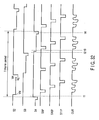
FIG. 32 is a waveform diagram of the major signals
in the solid image sensor including the pixel shown in
FIG. 29. As shown in FIG. 32, the pulse signals S2 to
S4 having the voltages indicating three values VL, VM,
and VH are applied to the selection lines 2 to 4.
In the three-valued voltage, VL is lowest, VM is higher
than VL, and VH is higher than VM.
The operation of the solid image sensor including
the pixel shown in FIG. 29 will next be described with
reference to FIG. 32.
The period in which the signals are read out of
all the pixels is referred to as one frame period.
In one frame period, the signals S2 to S4 of the
selection lines 2 to 4 rise to VH from VL and then rise
to VH from VL. In one frame period, the period in
which the signals S2 to S4 of the selection lines 2
to 4 indicate VH is the accumulation period of the
electrons. The period of VM is the readout period in
which the change of the threshold voltage of each pixel
is read out as the signal. Furthermore, the period
of VH is the reset period in which the electrons
integrated in each pixel are discharged.
For example, in the period in which the signal S2
of the selection line 2 indicates VM, three pixels 1
in the same row connected to the selection line 2 are
selected. When the signal S9P is set to the low level
in this period, the MOS transistor 9P is turned on, the
pixel column is selected, and one pixel is selected.
In this case, the current flows into the ground
potential via the power potential Vcc, current source
13, MOS transistor 9P, signal line 6, and selected
pixel, and the signal indicating the threshold voltage
of the selected pixel is outputted as the signal OUT
via the impedance conversion circuit 14. Furthermore,
when the signals S10P, S11P are successively set to
the low level, the MOS transistors 10P, 11P are
successively turned on, different pixel columns are
successively selected, the current flows from the
current source 13 via the signal lines 7, 8 and the
corresponding pixels 1 of the selected column, and the
signal indicating the threshold voltage of the selected
pixel is outputted as the signal OUT via the impedance
conversion circuit 14. The pixel row is changed and
successively subjected to this operation, so that
the signals are read out of all the pixels.
Moreover, after the signals are read out of three
pixels 1 in each pixel row, the signals S2 to S4 of
the selection lines 2 to 4 turn to VL, the electrons
are discharged to the n+-type diffusion region 55
from these three pixels, and the reset operation is
performed to prepare for the next accumulation of the
electrons.
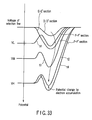
FIG. 33 shows the potential state in the section
taken along lines D-D', E-E', and F-F' in the sectional
view of FIG. 30 in the respective timings t1 to t4 in
the waveform diagram of FIG. 32.
The accumulation operation of the electrons in
each pixel, signal readout operation, and reset
operation will next be described in detail with
reference to the potential diagram of FIG. 33.
For example, in the timing t1 immediately after
the start of the accumulation period immediately after
the voltage signal S4 applied to the selection line 4
changes to VH from VL, as described above, for the
plurality of electron-hole pairs generated in
accordance with the incident light, the electrons are
accumulated and integrated centering on the minimum
point of the potential of the n-type well region 21
under the p-type diffusion region 44. Thereby, the
minimum point of the potential of the n-type well
region 21 and the maximum point of the potential of
the p-type diffusion region 44 are also modulated.
In the timing t2 immediately before the end of the
accumulation period, the potential minimum point of
the n-type well region 21 is higher than that of the
timing t1.
Subsequently, when the readout period is started,
and the pulse signal S4 applied to the selection line 4
changes to VM, the whole potential accordingly
increases in proportion to (VH-VM). Thereafter, when
the signal S9P indicates the low level, and the MOS
transistor 9P in FIG. 23 turns on, for three pixels 1
of the same column, the hole current flows from the
current source 13 via the pixel indicating the lowest
minimum point of the potential of the n+-type diffusion
region 43. In this case, while VH is applied to the
other selection lines 2, 3 excluding the selection line
4, VM is applied to the selection line 4, the potential
of the n+-type diffusion region 43 of the pixel
connected to the selection line 4 is highest, and
therefore the hole current flows via the pixel
connected to the selection line 4. The hole current
flowing at this time is shown by arrows a in FIG. 30.
That is, the source follower is thereby formed which
includes the power potential Vcc, current source 13,
MOS transistor 9P, signal line 6, and selected pixel,
and the potential is outputted as the signal OUT via
the impedance conversion circuit 14 in accordance with
the potential of the maximum point of the potential of
the p-type diffusion region 44 of the selected pixel.
In this case, since the maximum point of the potential
of the p-type diffusion region 44 is modulated by the
integrated value of the electron generated by the
incident light, all the pixels are scanned by the pixel
row selection circuit 5 and pixel column selection
circuit 12, the signal is successively read out of the
impedance conversion circuit 14, and thereby the video
signal can be obtained.
Subsequently, in the timing t4 after the readout
period ends and the pulse signal S4 applied to the
selection line 4 changes to VL, the potential of the
n+-type diffusion region 43 rises, and the electron
accumulated in the minimum point of the potential of
the n-type well region 21 under the p-type diffusion
region 44 is thereby discharged to the n+-type
diffusion region 55 via the n+-type diffusion
region 54.
Also in the fifth embodiment, each pixel is
constituted by one junction-type FET, and the structure
is simple and suitable for miniaturization as compared
with the CCD type. Additionally, the n-type well
region 21 in which the charges (electrons) are
accumulated forms a p-n junction with the peripheral
semiconductor region, and the predetermined voltage is
applied to the n-type well region 21, so that the
potential is not in the floating state. As a result,
after the charges (electrons) are discharged, the
background charges do not exist in the n-type well
region 21, and the conventional generation of the noise
by the fluctuation of the background charge amount can
be suppressed.
Moreover, since it is unnecessary to consider the
influence of the background charge, the density of the
impurity of the n-type well region 21 can be raised
to the certain degree. Therefore, the value of the
capacitance to the ground potential can sufficiently
be secured, the sufficient amount of signal charges
(electrons) can be accumulated, and the saturated
charge amount can be raised to the certain degree.
Furthermore, the junction gate FET is used in
which the polysilicon gate electrode is not used, and
the effect that the sensitivity to blue can be
prevented from dropping can therefore be obtained.
The photodiode including the p-type diffusion region 44
and n-type well region 21 under the diffusion region to
perform the photoelectric conversion, the photodiode
including the n-type well region 21 and p-type
substrate 20, the photodiode including the drain region
41 and n-type well region 21 under the drain region,
and the n-type well region 21 under the p-type embedded
region 26 in which the charges are accumulated are
disposed adjacent to one another, and integrated.
Therefore, the effect is obtained that the size of
the pixel can be miniaturized as compared with the
photodiodes and region formed separately from one
another.
(Sixth Embodiment)
FIG. 34 is a whole circuit diagram of the solid
image sensor according to a sixth embodiment of the
present invention.
The solid image sensor shown in FIG. 34 is
slightly different from that of FIG. 23 in the
constitutions of the pixel and pixel row selection
circuit, and the other constitution is similar to that
of FIG. 23.
In FIG. 34, each pixel 60 includes a junction-type
FET portion 60a for photoelectric conversion and
a junction-type FET portion 60b for discharging the
accumulated charges of the gate of a junction-type FET
portion 60a to the ground potential.
The gates of the junction-type FET portions 60a of
three pixels 60 of the same row are connected in common
to one corresponding line of a plurality of (three in
the present example) selection lines 2 to 4 for pixel
row selection. Moreover, the sources or drains and
gates of the junction-type FET portions 60b in three
pixels 60 of the same row are connected in common to
one corresponding line of a plurality of (three in
the present example) selection lines 16 to 18 for
electric discharge. The other source or drain of the
junction-type FET portion 60b is connected to the
corresponding gate of the junction-type FET portion
60a. It is to be noted that the selection lines 2 to 4
and 16 to 18 are connected to the pixel row selection
circuit 19.
In the solid image sensor of the sixth embodiment
shown in FIG. 34, when the light is incident, the
signal charges are accumulated in each pixel 60 in
accordance with each light amount, and the threshold
voltage of each pixel changes in accordance with the
accumulated signal charge amount. Moreover, when the
pulse signal outputted from the pixel row selection
circuit 19 is applied to any one of the selection lines
2 to 4, the pixel row is selected. Furthermore, when
the pulse signal outputted from the pixel column
selection circuit 12 is applied to any one of the
gates of the MOS transistors 9P to 11P, and the MOS
transistor is turned on, the pixel column is selected,
and thereby one pixel 60 is selected. In this case, as
shown by arrows in FIG. 34, the current path is formed
to extend to the ground potential via the power source
Vcc, current source 13, MOS transistor having the on
state (MOS transistor 10P in the present example),
signal line (signal line 7 in the present example), and
selected pixel, and the signal is outputted via the
impedance conversion circuit 14 in accordance with the
threshold voltage of the selected pixel.
When the pulse signal outputted from the pixel
row selection circuit 19 is applied to any one of the
signal lines 16 to 18, the signal charge accumulated in
each pixel 60 is discharged to the ground potential via
the junction-type FET portion 60b.
FIG. 35 is a pattern plan view showing the device
structure of one pixel in FIG. 34, and FIGS. 36 to 39
is different sectional views.
In the pixel of FIG. 29, the n+-type diffusion
region 43 and p-type diffusion region 44 are formed to
surround the source region 42 disposed in the middle.
On the other hand, in the sixth embodiment, the source
region 42 is formed to have the rectangular plane
pattern in the peripheral portion of the pixel region
defined by a two-dots chain line. Moreover, the
n+-type diffusion region 43, p-type diffusion region
44, and drain region 41 are extended in parallel with
the source region 42 in the horizontal direction in
FIG. 35.
Furthermore, an n+-type diffusion region 56
forming a drain for discharging the signal charges
(electrons) accumulated in the n-type well region 21
under the p-type diffusion region 44 is disposed
between the p-type diffusion regions 44 of the pixels
disposed adjacent to each other in the horizontal
direction in FIG. 35. Since the n+-type diffusion
region 56 is formed, the wiring layer 46 extended
in the vertical direction in FIG. 35 is folded in
a substantially U shape in a formed position of the n+
type diffusion region 56. Moreover, a wiring layer 57
is formed in parallel with the wiring layer 49 on the
second interlayer insulating film 48, and the n+-type
diffusion region 56 is connected to the wiring layer 57
via a contact 58. The wiring layer 57 corresponds to
the selection lines 16 to 18 in FIG. 34.
FIG. 40 is a waveform diagram of the major
signals in the solid image sensor shown in FIG. 34.
In FIG. 40, the signals S2, S3, S4 are outputted from
the pixel row selection circuit 19, and indicate the
waveforms of the pulse signals applied to the selection
lines 2 to 4 for row selection. The signals S16, S17,
S18 are outputted from the pixel row selection circuit
19, and indicate the waveforms of the pulse signals
applied to the selection lines 16 to 18 for electric
discharge. The signals S9P, S10P, S11P are outputted
from the pixel column selection circuit 12, and
indicate the waveforms of the pulse signals applied
to the gates of the MOS transistors 9P, 10P, 11P.
The signal OUT indicates the waveform of the signal
outputted from the impedance conversion circuit 14.
As shown in FIG. 40, the pulse signals S2 to S4 having
the voltages indicating two values VL, VH are applied
to the selection lines 2 to 4. Similarly, the pulse
signals S16 to S18 having the voltages indicating two
values VL and VH are applied to the selection lines 16
to 18. In the two-valued voltage, VL is lower than VH.
The operation of the solid image sensor of FIG. 34
will next be described with reference to FIG. 40.
The period in which the signals are read out of
all the pixels 60 is referred to as one frame period.
In one frame period, the signals S2 to S4 of the
selection lines 2 to 4 rise to VH from VL and then rise
to VH from VL. In one frame period, the period in
which the signals S2 to S4 of the selection lines 2
to 4 indicate VH is the accumulation period of the
signal charges (electrons). The period in which the
signals S2 to S4 indicate VL is the readout period.
Furthermore, the period in which the signals S2 to S4
indicate VL and the signals S16 to S18 of the selection
lines 16 to 18 indicate VH is a discharge period of the
signal charges (electrons). Therefore, the substantial
signal readout period is a period in which the signals
of the selection lines 2 to 4 and 16 to 18 indicate VL.
For example, in the period in which the signal S2
of the selection line 2 indicates the low level (VL),
three pixels 60 in the same row connected to the
selection line 2 are selected. When the signal S9P is
set to the low level in this period, the MOS transistor
9P is turned on, the pixel column is selected, and one
pixel 60 is selected. In this case, the current flows
into the ground potential via the power potential Vcc,
current source 13, MOS transistor 9P, signal line 6,
and selected pixel, and the signal indicating the
threshold voltage of the selected pixel is outputted as
the signal OUT via the impedance conversion circuit 14.
Furthermore, when the signals S10P, S11P are
successively set to the low level, the MOS transistors
10P, 11P are successively turned on, the different
pixel columns are successively selected, the current
flows via the signal lines 7, 8 and the corresponding
pixels 60 of the selected column, and the signal
indicating the threshold voltage of the selected pixel
is outputted as the signal OUT via the impedance
conversion circuit 14. The pixel row is changed and
successively subjected to this operation, so that the
signals are read out of all the pixels.
On the other hand, the signals S16 to S18 of the
selection lines 16 to 18 are set to VL, before the
signal readout period from three pixels 60 in each
pixel row is started. Furthermore, the signals S16 to
S18 of the selection lines 16 to 18 are set to VH,
before the signal readout period ends and the signals
S2 to S4 of the selection lines 2 to 4 are set to VL.
In the period in which the signals S2 to S4 of the
selection lines 2 to 4 indicate VL and the signals of
the selection lines 16 to 18 indicate VH, the electrons
accumulated in the n-type well region 21 under the
p-type diffusion region 44 are discharged to the
n+-type diffusion region 56, and the reset operation
is performed.
It is to be noted that the reset operation is
performed, when the signals S2 to S4 of the signal
lines 2 to 4 indicate VL and signals S16 to S18 of the
signal lines 16 to 18 indicate VH. Therefore, the
signals S16 to S18 of the signal lines 16 to 18 are
lowered to VL, before the signals S2 to S4 of the
signal lines 2 to 4 are set to VL and the readout
period is started.
FIG. 41 shows the potential states in the sections
taken along lines E-E', F-F', and G-G' of FIG. 37 in
the respective timings t1 to t4 in the signal waveform
diagram of FIG. 40.
The accumulation operation of the electrons in
each pixel, signal readout operation, and reset
operation will next be described in detail with
reference to the potential diagram of FIG. 41.
In the timing t1 immediately after the start of
the accumulation period immediately after the pulse
signal S4 applied to the selection line 4 changes to
VH, as described above, for the plurality of electron-hole
pairs generated in accordance with the incident
light, the electrons are accumulated and integrated in
the n-type well region 21 under the p-type diffusion
region 44. Thereby, the minimum point of the potential
of the n-type well region 21 and the maximum point of
the potential of the p-type diffusion region 44 are
also modulated. In the timing t2 immediately before
the end of the accumulation period, the potential of
the n-type well region 21 is higher than that of the
timing t1.
Subsequently, when the readout period is started,
and the pulse signal S4 applied to the selection line
4 changes to VL, the whole potential accordingly
increases in proportion to (VH-VL). Additionally,
since the p-type substrate 20 is fixed at the ground
potential, the potential of the substrate 20 is
constant and does not change. Thereafter, when the
signal S9 indicates the low level, and the MOS
transistor 9P in FIG. 34 turns on, for three pixels 60
of the same column, the hole current flows via the
pixel indicating the lowest potential of the n+-type
diffusion region 43. At this time, while VH is applied
to the other selection lines 2, 3 excluding the
selection line 4, VL is applied to the selection line
4, the potential of the n+-type diffusion region 43 of
the pixel connected to the selection line 4 is highest,
and therefore the hole current flows via the pixel
connected to the selection line 4. The current path
flowing at this time is shown by arrows a in FIG. 37.
That is, the source follower is thereby formed which
includes the power potential Vcc, current source 13,
MOS transistor 9P, signal line 6, and selected pixel,
and the potential is outputted as the signal OUT via
the impedance conversion circuit 14 in accordance with
the potential indicating the potential value of the
maximum point of the potential of the p-type diffusion
region 44 of the selected pixel 60. In this case,
since the maximum point of the potential of the p-type
diffusion region 44 is modulated by the integrated
value of the electrons generated by the incident light,
all the pixels are scanned by the pixel row selection
circuit 19 and pixel column selection circuit 12,
the signal is successively read out of the impedance
conversion circuit 14, and thereby the video signal can
be obtained.
Subsequently, in the timing t4 after the pulse
signal S4 applied to the selection line 4 indicates VL
and the pulse signal S18 applied to the selection line
18 changes to VH from VL, the electrons accumulated in
the n-type well region 21 under the p-type diffusion
region 44 in FIG. 36 is discharged to the n+-type
semiconductor region 56 in a path shown by an arrow b
in the drawings. Thereby, the potential of the p-type
diffusion region 44 drops, and the reset operation is
performed.
That is, in the sixth embodiment, the photoelectrically
converted and accumulated electrons are
discharged to the n+-type diffusion region 56 formed in
the surface region of the n-type well region 21 without
being discharged to the drain region 41 as in the
fourth embodiment, or to the n+-type diffusion region
55 as in the fifth embodiment.
It is to be noted that both the n+- type diffusion
regions 43 and 56 are formed in the surface of the
n-type well region 21. Therefore, when the voltages
applied to the regions differ from each other, the
current possibly flows between the regions. To prevent
this, when the impurity density of the n-type well
region 21 surface is adjusted to obtain a high
resistance, the current value can be set to be small,
and therefore an adverse influence by the flowing of
the current can be avoided.
FIGS. 42 and 43 two-dimensionally show the
potential state in the section along line XXXVI-XXXVI
in FIG. 35. It is to be noted that FIG. 42 shows the
state in the timing t3 immediately after the readout
start, and FIG. 43 shows the state in the timing t4 at
the electric discharge time. Moreover, the voltage
shown in the drawing indicates the potential. When the
voltage increases, the potential deepens.
As shown in FIG. 42, immediately after the readout
start (t = t3), the saddle point P of the potential
is positioned in the n-type well region 21 under the
n+-type diffusion region 56, the signal charges
(electrons) are accumulated in the vicinity of the
p-type diffusion region 44, and the path in which
the hole current flows is formed in the vicinity of
the p-type diffusion region 44.
At the electric discharge time (t = t4), as shown
by a broken-line arrow in FIG. 43, the potential
successively rises toward the n+-type diffusion region
56 from below the p-type diffusion region 44, and the
electron charges accumulated under the p-type diffusion
region 44 are discharged to the n+-type diffusion
region 56. It is to be noted that the supply of the
voltage VH of 5V to the n+-type diffusion region 56 at
the electric discharge time has been described in this
example.
As described above, even in the solid image sensor
of the sixth embodiment, each pixel is substantially
constituted by one junction-type FET, and the structure
is simple and suitable for miniaturization as compared
with the CCD type. Additionally, the n-type well
region 21 in which the charges (electrons) are
accumulated forms a p-n junction with the peripheral
semiconductor region, and the predetermined voltage
is applied to the n-type well region 21, so that the
potential is not in the floating state. As a result,
after the charges (electrons) are discharged, the
background charges do not exist in the n-type well
region 21, and the conventional generation of the noise
by the fluctuation of the background charge amount can
be suppressed.
Moreover, since it is unnecessary to consider the
influence of the background charge, the density of the
impurity of the n-type well region 21 can be raised to
the certain degree. Therefore, the value of the
capacity to ground can sufficiently be secured, the
sufficient amount of signal charges (electrons) can
be accumulated, and the saturated charge amount can
therefore be raised by the certain degree.
Furthermore, the junction gate FET is used in
which the polysilicon gate electrode is not used,
and the effect that the sensitivity to blue can be
prevented from dropping can therefore be obtained.
The photodiode including the p-type diffusion region 44
and n-type well region 21 under the diffusion region to
perform the photoelectric conversion, the photodiode
including the n-type well region 21 and p-type
substrate 20, and n-type well region 21 under the
p-type embedded region 26 in which the charges are
accumulated are disposed adjacent to one another, and
integrated. Therefore, the effect is obtained that the
size of the pixel can be miniaturized as compared with
the photodiodes and region formed separately from one
another.
(Application Example)
FIG. 44 shows a schematic block constitution of
a control circuit of an electronic camera using the
solid image sensor according to the first to sixth
embodiments. In FIG. 44, reference numeral 81 denotes
an integrated circuit chip for solid image sensing in
which in addition to the solid image sensor according
to the first to sixth embodiment, a timing generator
and control circuit such as an A/D conversion circuit
are integrated, and 82 denotes an integrated circuit
chip for camera digital signal processor (DSP).
The integrated circuit chip 82 supplies commands
and various types of control signals to the integrated
circuit chip 81. The integrated circuit chip 81
supplies the image signal read by photoelectric
conversion as a digital signal to the integrated
circuit chip 82. The integrated circuit chip 82
subjects the supplied image signal to various types of
signal processing such as white balance adjustment and
gamma processing, and outputs a digital image signal.
FIGS. 45A and 45B are plan and sectional views of
a camera module in which the integrated circuit chip 81
and integrated circuit chip 82 shown in FIG. 44 are
formed as a module together with lenses. In this
module, the integrated circuit chip for solid image
pickup 81 contained in a container 92 is laid on
a surface side of a base 91, and an infrared ray
(IR) removal filter 93 is attached onto the chip.
Furthermore, a lens module 95 including a focusing
lens 94 for irradiating the surface of the integrated
circuit chip 81 with light is attached onto the IR
removal filter 93. Moreover, the integrated circuit
chip 82 is laid on a back surface side of the base 91,
and the integrated circuit chip 81 is electrically
connected to the integrated circuit chip 82.
Additionally, the base 91 is connected to a flexible
cable 96, and a signal is transmitted/received with
respect to the outside via the flexible cable 96.