EP1309012A2 - Integrated Schottky barrier diode and manufacturing method thereof - Google Patents
Integrated Schottky barrier diode and manufacturing method thereof Download PDFInfo
- Publication number
- EP1309012A2 EP1309012A2 EP20020024472 EP02024472A EP1309012A2 EP 1309012 A2 EP1309012 A2 EP 1309012A2 EP 20020024472 EP20020024472 EP 20020024472 EP 02024472 A EP02024472 A EP 02024472A EP 1309012 A2 EP1309012 A2 EP 1309012A2
- Authority
- EP
- European Patent Office
- Prior art keywords
- schottky barrier
- barrier diode
- diode
- layer
- electrode
- Prior art date
- Legal status (The legal status is an assumption and is not a legal conclusion. Google has not performed a legal analysis and makes no representation as to the accuracy of the status listed.)
- Withdrawn
Links
- 230000004888 barrier function Effects 0.000 title claims abstract description 103
- 238000004519 manufacturing process Methods 0.000 title claims abstract description 20
- 239000000758 substrate Substances 0.000 claims abstract description 38
- 150000001875 compounds Chemical class 0.000 claims abstract description 14
- 239000004065 semiconductor Substances 0.000 claims abstract description 14
- 239000012535 impurity Substances 0.000 claims description 40
- 238000000034 method Methods 0.000 claims description 20
- JBRZTFJDHDCESZ-UHFFFAOYSA-N AsGa Chemical compound [As]#[Ga] JBRZTFJDHDCESZ-UHFFFAOYSA-N 0.000 claims description 19
- 229910001218 Gallium arsenide Inorganic materials 0.000 claims description 18
- 238000005468 ion implantation Methods 0.000 claims description 10
- 239000004642 Polyimide Substances 0.000 abstract description 17
- 229920001721 polyimide Polymers 0.000 abstract description 17
- 238000002513 implantation Methods 0.000 abstract description 5
- 239000002184 metal Substances 0.000 description 30
- 229910052751 metal Inorganic materials 0.000 description 30
- 229920002120 photoresistant polymer Polymers 0.000 description 22
- 239000010931 gold Substances 0.000 description 11
- 230000015572 biosynthetic process Effects 0.000 description 9
- 238000005530 etching Methods 0.000 description 9
- 239000000543 intermediate Substances 0.000 description 9
- 150000004767 nitrides Chemical class 0.000 description 9
- 230000008569 process Effects 0.000 description 9
- 239000002131 composite material Substances 0.000 description 4
- 238000007747 plating Methods 0.000 description 4
- 238000000926 separation method Methods 0.000 description 4
- 238000000151 deposition Methods 0.000 description 3
- 238000013461 design Methods 0.000 description 3
- 229910052581 Si3N4 Inorganic materials 0.000 description 2
- 229910052737 gold Inorganic materials 0.000 description 2
- 230000003071 parasitic effect Effects 0.000 description 2
- 238000000059 patterning Methods 0.000 description 2
- 230000009467 reduction Effects 0.000 description 2
- HQVNEWCFYHHQES-UHFFFAOYSA-N silicon nitride Chemical compound N12[Si]34N5[Si]62N3[Si]51N64 HQVNEWCFYHHQES-UHFFFAOYSA-N 0.000 description 2
- 238000005549 size reduction Methods 0.000 description 2
- ZOXJGFHDIHLPTG-UHFFFAOYSA-N Boron Chemical compound [B] ZOXJGFHDIHLPTG-UHFFFAOYSA-N 0.000 description 1
- YZCKVEUIGOORGS-UHFFFAOYSA-N Hydrogen atom Chemical compound [H] YZCKVEUIGOORGS-UHFFFAOYSA-N 0.000 description 1
- 229910045601 alloy Inorganic materials 0.000 description 1
- 239000000956 alloy Substances 0.000 description 1
- 238000000137 annealing Methods 0.000 description 1
- 230000008901 benefit Effects 0.000 description 1
- 229910052796 boron Inorganic materials 0.000 description 1
- 230000015556 catabolic process Effects 0.000 description 1
- 238000005229 chemical vapour deposition Methods 0.000 description 1
- 238000000576 coating method Methods 0.000 description 1
- 238000004891 communication Methods 0.000 description 1
- 239000000470 constituent Substances 0.000 description 1
- 238000007796 conventional method Methods 0.000 description 1
- 230000001419 dependent effect Effects 0.000 description 1
- 238000001312 dry etching Methods 0.000 description 1
- 230000005669 field effect Effects 0.000 description 1
- PCHJSUWPFVWCPO-UHFFFAOYSA-N gold Chemical compound [Au] PCHJSUWPFVWCPO-UHFFFAOYSA-N 0.000 description 1
- 230000006872 improvement Effects 0.000 description 1
- WABPQHHGFIMREM-UHFFFAOYSA-N lead(0) Chemical group [Pb] WABPQHHGFIMREM-UHFFFAOYSA-N 0.000 description 1
- 238000012423 maintenance Methods 0.000 description 1
- 235000012054 meals Nutrition 0.000 description 1
- 150000002739 metals Chemical class 0.000 description 1
- 238000012986 modification Methods 0.000 description 1
- 230000004048 modification Effects 0.000 description 1
- 229910052759 nickel Inorganic materials 0.000 description 1
- 230000010355 oscillation Effects 0.000 description 1
- 238000004806 packaging method and process Methods 0.000 description 1
- 229910052697 platinum Inorganic materials 0.000 description 1
- 229920000642 polymer Polymers 0.000 description 1
- 238000012545 processing Methods 0.000 description 1
- 239000011347 resin Substances 0.000 description 1
- 229920005989 resin Polymers 0.000 description 1
- 229910052719 titanium Inorganic materials 0.000 description 1
- 238000001721 transfer moulding Methods 0.000 description 1
Images

Classifications
-
- H—ELECTRICITY
- H01—ELECTRIC ELEMENTS
- H01L—SEMICONDUCTOR DEVICES NOT COVERED BY CLASS H10
- H01L27/00—Devices consisting of a plurality of semiconductor or other solid-state components formed in or on a common substrate
- H01L27/02—Devices consisting of a plurality of semiconductor or other solid-state components formed in or on a common substrate including semiconductor components specially adapted for rectifying, oscillating, amplifying or switching and having at least one potential-jump barrier or surface barrier; including integrated passive circuit elements with at least one potential-jump barrier or surface barrier
- H01L27/04—Devices consisting of a plurality of semiconductor or other solid-state components formed in or on a common substrate including semiconductor components specially adapted for rectifying, oscillating, amplifying or switching and having at least one potential-jump barrier or surface barrier; including integrated passive circuit elements with at least one potential-jump barrier or surface barrier the substrate being a semiconductor body
- H01L27/08—Devices consisting of a plurality of semiconductor or other solid-state components formed in or on a common substrate including semiconductor components specially adapted for rectifying, oscillating, amplifying or switching and having at least one potential-jump barrier or surface barrier; including integrated passive circuit elements with at least one potential-jump barrier or surface barrier the substrate being a semiconductor body including only semiconductor components of a single kind
- H01L27/0814—Diodes only
-
- H—ELECTRICITY
- H01—ELECTRIC ELEMENTS
- H01L—SEMICONDUCTOR DEVICES NOT COVERED BY CLASS H10
- H01L24/00—Arrangements for connecting or disconnecting semiconductor or solid-state bodies; Methods or apparatus related thereto
- H01L24/01—Means for bonding being attached to, or being formed on, the surface to be connected, e.g. chip-to-package, die-attach, "first-level" interconnects; Manufacturing methods related thereto
- H01L24/02—Bonding areas ; Manufacturing methods related thereto
- H01L24/04—Structure, shape, material or disposition of the bonding areas prior to the connecting process
- H01L24/05—Structure, shape, material or disposition of the bonding areas prior to the connecting process of an individual bonding area
-
- H—ELECTRICITY
- H01—ELECTRIC ELEMENTS
- H01L—SEMICONDUCTOR DEVICES NOT COVERED BY CLASS H10
- H01L27/00—Devices consisting of a plurality of semiconductor or other solid-state components formed in or on a common substrate
- H01L27/02—Devices consisting of a plurality of semiconductor or other solid-state components formed in or on a common substrate including semiconductor components specially adapted for rectifying, oscillating, amplifying or switching and having at least one potential-jump barrier or surface barrier; including integrated passive circuit elements with at least one potential-jump barrier or surface barrier
- H01L27/04—Devices consisting of a plurality of semiconductor or other solid-state components formed in or on a common substrate including semiconductor components specially adapted for rectifying, oscillating, amplifying or switching and having at least one potential-jump barrier or surface barrier; including integrated passive circuit elements with at least one potential-jump barrier or surface barrier the substrate being a semiconductor body
- H01L27/06—Devices consisting of a plurality of semiconductor or other solid-state components formed in or on a common substrate including semiconductor components specially adapted for rectifying, oscillating, amplifying or switching and having at least one potential-jump barrier or surface barrier; including integrated passive circuit elements with at least one potential-jump barrier or surface barrier the substrate being a semiconductor body including a plurality of individual components in a non-repetitive configuration
- H01L27/0605—Devices consisting of a plurality of semiconductor or other solid-state components formed in or on a common substrate including semiconductor components specially adapted for rectifying, oscillating, amplifying or switching and having at least one potential-jump barrier or surface barrier; including integrated passive circuit elements with at least one potential-jump barrier or surface barrier the substrate being a semiconductor body including a plurality of individual components in a non-repetitive configuration integrated circuits made of compound material, e.g. AIIIBV
-
- H—ELECTRICITY
- H01—ELECTRIC ELEMENTS
- H01L—SEMICONDUCTOR DEVICES NOT COVERED BY CLASS H10
- H01L29/00—Semiconductor devices adapted for rectifying, amplifying, oscillating or switching, or capacitors or resistors with at least one potential-jump barrier or surface barrier, e.g. PN junction depletion layer or carrier concentration layer; Details of semiconductor bodies or of electrodes thereof ; Multistep manufacturing processes therefor
- H01L29/66—Types of semiconductor device ; Multistep manufacturing processes therefor
- H01L29/66007—Multistep manufacturing processes
- H01L29/66075—Multistep manufacturing processes of devices having semiconductor bodies comprising group 14 or group 13/15 materials
- H01L29/66083—Multistep manufacturing processes of devices having semiconductor bodies comprising group 14 or group 13/15 materials the devices being controllable only by variation of the electric current supplied or the electric potential applied, to one or more of the electrodes carrying the current to be rectified, amplified, oscillated or switched, e.g. two-terminal devices
- H01L29/6609—Diodes
- H01L29/66143—Schottky diodes
-
- H—ELECTRICITY
- H01—ELECTRIC ELEMENTS
- H01L—SEMICONDUCTOR DEVICES NOT COVERED BY CLASS H10
- H01L29/00—Semiconductor devices adapted for rectifying, amplifying, oscillating or switching, or capacitors or resistors with at least one potential-jump barrier or surface barrier, e.g. PN junction depletion layer or carrier concentration layer; Details of semiconductor bodies or of electrodes thereof ; Multistep manufacturing processes therefor
- H01L29/66—Types of semiconductor device ; Multistep manufacturing processes therefor
- H01L29/86—Types of semiconductor device ; Multistep manufacturing processes therefor controllable only by variation of the electric current supplied, or only the electric potential applied, to one or more of the electrodes carrying the current to be rectified, amplified, oscillated or switched
- H01L29/861—Diodes
- H01L29/872—Schottky diodes
-
- H—ELECTRICITY
- H01—ELECTRIC ELEMENTS
- H01L—SEMICONDUCTOR DEVICES NOT COVERED BY CLASS H10
- H01L2224/00—Indexing scheme for arrangements for connecting or disconnecting semiconductor or solid-state bodies and methods related thereto as covered by H01L24/00
- H01L2224/01—Means for bonding being attached to, or being formed on, the surface to be connected, e.g. chip-to-package, die-attach, "first-level" interconnects; Manufacturing methods related thereto
- H01L2224/02—Bonding areas; Manufacturing methods related thereto
- H01L2224/04—Structure, shape, material or disposition of the bonding areas prior to the connecting process
- H01L2224/04042—Bonding areas specifically adapted for wire connectors, e.g. wirebond pads
-
- H—ELECTRICITY
- H01—ELECTRIC ELEMENTS
- H01L—SEMICONDUCTOR DEVICES NOT COVERED BY CLASS H10
- H01L2224/00—Indexing scheme for arrangements for connecting or disconnecting semiconductor or solid-state bodies and methods related thereto as covered by H01L24/00
- H01L2224/01—Means for bonding being attached to, or being formed on, the surface to be connected, e.g. chip-to-package, die-attach, "first-level" interconnects; Manufacturing methods related thereto
- H01L2224/42—Wire connectors; Manufacturing methods related thereto
- H01L2224/44—Structure, shape, material or disposition of the wire connectors prior to the connecting process
- H01L2224/45—Structure, shape, material or disposition of the wire connectors prior to the connecting process of an individual wire connector
- H01L2224/45001—Core members of the connector
- H01L2224/45099—Material
- H01L2224/451—Material with a principal constituent of the material being a metal or a metalloid, e.g. boron (B), silicon (Si), germanium (Ge), arsenic (As), antimony (Sb), tellurium (Te) and polonium (Po), and alloys thereof
- H01L2224/45138—Material with a principal constituent of the material being a metal or a metalloid, e.g. boron (B), silicon (Si), germanium (Ge), arsenic (As), antimony (Sb), tellurium (Te) and polonium (Po), and alloys thereof the principal constituent melting at a temperature of greater than or equal to 950°C and less than 1550°C
- H01L2224/45144—Gold (Au) as principal constituent
-
- H—ELECTRICITY
- H01—ELECTRIC ELEMENTS
- H01L—SEMICONDUCTOR DEVICES NOT COVERED BY CLASS H10
- H01L2224/00—Indexing scheme for arrangements for connecting or disconnecting semiconductor or solid-state bodies and methods related thereto as covered by H01L24/00
- H01L2224/01—Means for bonding being attached to, or being formed on, the surface to be connected, e.g. chip-to-package, die-attach, "first-level" interconnects; Manufacturing methods related thereto
- H01L2224/42—Wire connectors; Manufacturing methods related thereto
- H01L2224/47—Structure, shape, material or disposition of the wire connectors after the connecting process
- H01L2224/48—Structure, shape, material or disposition of the wire connectors after the connecting process of an individual wire connector
- H01L2224/484—Connecting portions
- H01L2224/48463—Connecting portions the connecting portion on the bonding area of the semiconductor or solid-state body being a ball bond
-
- H—ELECTRICITY
- H01—ELECTRIC ELEMENTS
- H01L—SEMICONDUCTOR DEVICES NOT COVERED BY CLASS H10
- H01L2924/00—Indexing scheme for arrangements or methods for connecting or disconnecting semiconductor or solid-state bodies as covered by H01L24/00
- H01L2924/10—Details of semiconductor or other solid state devices to be connected
- H01L2924/11—Device type
- H01L2924/12—Passive devices, e.g. 2 terminal devices
- H01L2924/1203—Rectifying Diode
- H01L2924/12032—Schottky diode
-
- H—ELECTRICITY
- H01—ELECTRIC ELEMENTS
- H01L—SEMICONDUCTOR DEVICES NOT COVERED BY CLASS H10
- H01L2924/00—Indexing scheme for arrangements or methods for connecting or disconnecting semiconductor or solid-state bodies as covered by H01L24/00
- H01L2924/10—Details of semiconductor or other solid state devices to be connected
- H01L2924/11—Device type
- H01L2924/14—Integrated circuits
Definitions
- This invention relates to an integrated Schottky barrier diode chip made of a compound semiconductor for use in a high frequency circuit, specifically to an integrated Schottky barrier diode chip that includes an insulating region electrically separating portions of a diode of the chip, and a manufacturing method thereof.
- FET field effect transistor
- GaAs gallium arsenide
- MMIC monolithic microwave integrated circuit
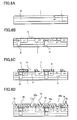
- FIG. 1A is a plan view of a conventional integrated Schottky barrier diode chip, and FIG 1B is its equivalent circuit.
- This type of integrated Schottky barrier diode is referred to as a Tee type, and has two Schottky barrier diodes 40a, 40b integrated in a chip.
- This chip also has a common electrode 36a and its related terminal 34, a cathode electrode 36b and its related terminal 35, and an anode electrode 36c and its related terminal 32.
- These electrodes 36a, 36b, 36c are indicated by the areas encircled by unevenly broken lines in the figure.
- the two Schottky barrier diodes 40a, 40b share the common electrode 36a.
- the common electrode 36a serves as a cathode electrode of the Schottky barrier diode 40a, the anode of which is the anode electrode 36c, and serves as an anode of the Schottky barrier diode 40b, the cathode of which is the cathode electrode 36b.
- the terminals are the areas of the corresponding electrodes that are used for external connection. Typically, those are the areas for wire bonding, and indicated by the circles in FIG. 1A.
- This configuration provides a circuit shown in FIG. 1B. Namely, the cathode of the Schottky barrier diode 40a, the anode of which is the anode terminal 32, is connected to the anode of the Schottky barrier diode 40b, the cathode of which is the cathode terminal 35.
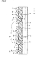
- FIG. 2 is a cross-sectional view of the integrated Schottky barrier diode chip of FIG. 1A. This cross-section is along the arrow in FIG. 1 and intersects operation areas of the two diodes.
- An n+ epitaxial layer 22 (Si + 5 x 10 18 cm -3 ) is disposed on an undoped GaAs substrate 21 and has a thickness of about 6 ⁇ m.
- An n epitaxial layer 23 (Si + 1.3 x 10 17 cm -3 ) is disposed on the n+ epitaxial layer 22 and has a thickness of about 350 nm. This n epitaxial layer 23 serves as an operation layer of the Schottky barrier diodes.
- An ohmic electrode 28 is a disposed directly on the n+ epitaxial layer 22 and forms an ohmic contact with the n+ epitaxial layer 22.
- This first metal layer is made of a AuGe/Ni/Au composite metal layer.
- a second metal layer 33 made of Ti/Pt/Au composite layer, forms a Schottky contact with the n epitaxial layer 23 in a Schottky contact region 31a of the anode portion of the diode, and forms a contact with the ohmic electrode 28 in the cathode portion of the diode.
- a third metal layer 36 is a Au metal layer, which is formed by plating using the second metal layer 33 as a base electrode, and completely covers the second metal layer 33. Portions 36a, 36b, 36c of the third metal layer 36 serve as the common electrode 36a, the cathode electrode 36b and the anode electrode 36c, respectively.
- the Schottky contact region 31a has a circular shape with a diameter of about 10 ⁇ m, as shown in FIG. 1.
- the first metal layer 28 surrounds the Schottky contact region 31a.
- the first and second metal layers are formed by vapor depositing the constituent metals separately.
- a lead wire is bonded to the electrode surface as shown by reference numerals 32, 34 and 35 in FIG. 2.
- the Schottky barrier diode on the left 40b has the cathode electrode 36b, which serves a cathode of this left diode and the common electrode 36a, which serves as an anode of this left diode
- the Schottky barrier diode on the right 40a has the anode electrode 36c, which serves an anode of this right diode and the common electrode 36a, which serves as a cathode of this right diode.
- the common electrode 36a works as an anode electrode of the diode 40b and a cathode electrode of the diode 40a.
- the second metal layer 33 on the Schottky contact regions 31a is at an anode voltage
- the n+ and n epitaxial layers are at a cathode voltage
- a polyimide layer 30 is required as an insulating layer under the second and third metal layers 33, 36, which are at the anode voltage, at locations in which the metal layers 33, 36 intersect the portions of the epitaxial layers 22, 23, which are at the cathode voltage.
- the thickness of the polyimide layer 30 needs to be as much as 6-7 ⁇ m because this intersection area is large and the resultant parasitic capacitance must be reduced by increasing the thickness.
- Polyimide is used as the insulating layer because it has a low dielectric constant and suitable for a thick layer formation.
- this configuration needs a trench 26 that separates the portions of the epitaxial layers 22, 23, which are at the cathode voltage, from the portions of the epitaxial layers 22, 23, which are at the anode voltage. This is an inevitable requirement when more than two diodes are formed in one chip.
- the trenches 26 reach the undoped gallium arsenide substrate 21, and are filled with the same polyimide used for the polyimide layer 30.
- the ohmic electrode 28 needs to form a direct contact with the n+ epitaxial layer for reducing the associated electric resistance. For this reason, a mesa etching is required to expose the n+ epitaxial layer 22 that is covered by the n epitaxial layer 23.
- the n epitaxial layer 23 at the Schottky contact region is also required to be etched to precisely the thickness of 250 nm for good electric characteristics.
- the Schottky barrier diode of the conventional configuration described above has a few disadvantages.
- the object of this invention is directed to an integrated Schottky barrier diode chip that is smaller and is fabricated by a simpler process than the conventional integrated Schottky barrier diode chip.
- the invention provides an integrated Schottky barrier diode chip including a compound semiconductor substrate, an operation layer formed on the substrate, and a plurality of Schottky barrier diodes formed on the substrate.
- the device also includes an insulating region formed in the operation layer, which electrically separates a first portion of the operation layer of one of the plurality of Schottky barrier diodes from a second portion of the operation layer of that Schottky barrier diodes.
- the device further includes an impurity region formed in the operation layer, which electrically communicates with one of the first and second portions of the operation layer of that Schottky barrier diode.
- the invention also provides an integrated Schottky barrier diode chip that has a first Schottky barrier diode and a second Schottky barrier diode each formed on a compound semiconductor substrate.
- the device includes an operation layer formed on the substrate, an anode electrode, a cathode electrode and a common electrode.
- a first insulating region and a first impurity region are formed in the operation layer for the first Schottky barrier diode.
- a second insulating region and a second impurity region are formed in the operation layer for the second Schottky barrier diode.
- the first insulating region electrically separates a portion of the operation layer of the first diode that is connected to the anode electrode from a portion of the operation layer of the first diode that is connected to the common electrode
- the second insulating region electrically separates a portion of the operation layer of the second diode that is connected to the common electrode from a portion of the operation layer of the second diode that is connected to the cathode electrode.
- the first impurity region electrically communicates with the operation layer of the first diode that is connected to the common electrode
- the second impurity region electrically communicates with the operation layer of the second diode that is that is connected to the cathode electrode.
- the invention further provides a method of manufacturing an integrated Schottky barrier diode chip having a plurality of Schottky barrier diodes.
- the method includes forming a plurality of insulating regions on a compound semiconductor substrate by an ion implantation, and forming a Schottky barrier diode on each of the plurality of the insulating regions so that each of the insulating regions electrically separates a first portion of the corresponding diode from a second portion of the corresponding diode.
- the invention also provides a method of manufacturing an integrated Schottky barrier diode chip having a plurality of Schottky barrier diodes.
- the method includes forming an epitaxial layer of a conduction type on an undoped compound semiconductor substrate, forming a plurality of insulating regions in the epitaxial layer by an ion implantation, and forming a Schottky barrier diode on each of the plurality of the insulating regions so that each of the insulating regions electrically separates a first portion of the epitaxial layer of the corresponding diode from a second portion of the epitaxial layer of the corresponding diode.
- Both of the embodiments include an undoped GaAs substrate 1, an anode electrode 16c, a cathode electrode 16b, a common electrode 16a, Schottky barrier diodes 20a, 20b and an insulating region 6.
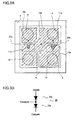
- FIG. 3A is a plan view of an integrated Schottky barrier diode chip of the first embodiment of this invention
- FIG. 3B is an equivalent circuit of the device of FIG. 3A.
- This integrated Schottky barrier diode is a Tee type device, and has two Schottky barrier diodes 20a, 20b integrated in a chip.
- This chip also has a common electrode 16a and its related terminal 14, a cathode electrode 16b and its related terminal 15, and an anode electrode 16c and its related terminal 12. These electrodes 16a, 16b, 16c are indicated by the areas encircled by unevenly broken lines in the figure.
- the two Schottky barrier diodes 20a, 20b share the common electrode 16a.
- the common electrode 16a serves as a cathode of the Schottky barrier diode 20a, the anode of which is the anode electrode 16c, and serves as an anode of the Schottky barrier diode 20b, the cathode of which is the cathode electrode 16b.
- the terminals are the areas of the corresponding electrodes that are used for external connection. Typically, those are the areas for wire bonding, and indicated by the circles in FIG. 3A.
- This configuration provides a circuit shown in FIG. 3B. Namely, the cathode of the Schottky barrier diode 20a, the anode of which is the anode terminal 12, is connected to the anode of the Schottky barrier diode 20b, the cathode of which is the cathode terminal 15.
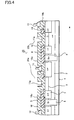
- FIG. 4 is a cross-sectional view of the integrated Schottky barrier diode chip of FIG. 3A. This cross-section is along the arrow in FIG. 3A and intersects operation areas of the two diodes.
- An n+ epitaxial layer 2 (Si + 5 x 10 18 cm -3 ) is disposed on an undoped GaAs substrate 1 and has a thickness of about 500 nm.
- An n epitaxial layer 3 (Si + 1.3 x 10 17 cm -3 ) is disposed on the n+ epitaxial layer 2 and has a thickness of about 250 nm. This n epitaxial layer 3 is an operation layer of the Schottky barrier diodes.
- Impurity region 7 of a high concentration (Si + 1 x 10 18 cm -3 ) is formed in the n epitaxial layer 3 under an ohmic electrode 8, and reaches the n+ epitaxial layer 2.
- the impurity region 7 surrounds a Schottky contact region 11a, which is circular as shown in FIG. 3A, and overlaps with the ohmic electrode 8, which is indicated by the area encircled by the broken lines in FIG. 3A.
- the impurity region 7 is larger than the ohmic electrode 8 and extends outside the area covered by the ohmic electrode 8.
- the distance between the edge of the Schottky contact region 11a and the edge of the impurity region 7 is about 1 ⁇ m, and the distance between the edge of the Schottky contact region 11a and the edge of the ohmic electrode 8 is about 2 ⁇ m. Because of this impurity region 7, which reaches the n+ epitaxial layer 2 form the surface of the n epitaxial layer 3, there is no need for forming a mesa structure, which is required for forming an ohmic contact with the n+ epitaxial layer in the conventional device as shown in FIG. 2. Accordingly, the device of the first embodiment has a planar configuration.
- the ohmic electrode 8 is a disposed directly on the impurity region 7 and forms an ohmic contact with the n+ epitaxial layer 2 through the impurity region 7.
- This first metal layer is made of a AuGe/Ni/Au composite metal layer and has a hole corresponding to the Schottky contact region 11a, as shown by the broken line in FIG. 3A.
- Portions 16a, 16b, 16c of second metal layer 16 serve as the common electrode 16a, the cathode electrode 16b and the anode electrode 16c, respectively.
- the Schottky contact region 11a has a circular shape with a diameter of about 10 ⁇ m, as shown in FIG. 3A.
- the thickness (250 nm) of the n epitaxial layer 3, which is an operation layer of the Schottky barrier diode, is determined so that proper device characteristics, including a high breakdown voltage, are obtained. Because of the planar configuration of this embodiment, the thickness control of the operation layer or the mesa etching is not needed. Then the device of the first embodiment is much easier to produce and more reliable than the conventional device that requires very precise etching control of the operation layer and complicated mesa etching. Accordingly, the integrated Schottky barrier diode chip of this embodiment has improved device characteristics.
- the common electrode 16a is disposed diagonally on the chip, and two areas for wire bonding are provided at both diagonal ends of the common electrode. Only one area needs to be wire-bonded for external connection and become a common terminal 14. This configuration makes it easier to mount the integrated Schottky barrier diode chip of this embodiment on a package frame, a print board or the like, because the common electrode 16a is accessible from two different directions for wire bonding.
- the Schottky barrier diode 20a on the left has the anode electrode 16c, which serves as an anode of this left diode and the common electrode 16a, which serves as a cathode of this left diode
- the Schottky diode 20b on the right has the cathode electrode 16b, which serves as a cathode of this right diode and the common electrode 16a, which serves as an anode of this right diode.
- the common electrode 16a works as a cathode electrode of the diode 20a and an anode electrode of the diode 20b.
- the second metal layer 16 on the Schottky contact regions 11a is at an anode voltage
- the n+ and n epitaxial layers are at a cathode voltage.
- An insulating region 6 is formed for each of the anode and cathode electrodes 16c, 16b, and surrounds the corresponding electrodes 16c, 16b.
- the insulating layer 6 electrically separates the portions of the n+ and n epitaxial layers 2, 3 that are at the anode voltage form the portions of the n+ and n epitaxial layers 2, 3 that are at the cathode voltage.
- each of the insulating regions 6 reaches the undoped GaAs substrate 1, which is essentially an insulating substrate.
- the insulating region 6 replaces the conventional trench structure of FIG. 2.
- This insulating film 5 replaces the conventional polyimide layer of FIG. 2.
- the silicon nitride insulating film 5 is thinner and has a higher dielectric constant than the polyimide layer of the conventional device, it can be used as an insulating layer because it occupies a smaller area than the conventional polyimide layer.
- the area of the intersection between the second metal layer 16 that is at the anode voltage and the portion of the n and n+ epitaxial layers 2, 3 and the corresponding impurity regions 6 that are at the cathode voltage are much smaller than that of the conventional device.
- This is made possible thanks to the smaller process error margin due to the planar configuration of this embodiment, which are free from the mesa structure and the tall polyimide insulating layer that require larger process error margin and, thus, a larger separation between the Schottky contact region and the ohmic electrode, which results in a larger area for generating parasitic capacitance.
- the distance between the edge of the Schottky contact region 11a and the edge of the ohmic electrode 8 in this embodiment is 2 ⁇ m, which is much shorter than 7 ⁇ m, the corresponding distance of the conventional device. Furthermore, the distance between the edge of the Schottky region 11a and the edge of the impurity region 7 is 1 ⁇ m. Since the impurity region 7, which serves as a carrier path, has the electronic conduction properties similar to the ohmic electrode 8, the effective separation in this embodiment is about one seventh of the conventional device. This shorter separation also contributes to reduction of the electric resistance between the Schottky contact region 11a and the ohmic electrode 8/impurity region 7, and thus improvement of high frequency device characteristics.
- the configuration described above does not have a deep trench or tall polyimide layer on the surface of the GaAs chip. Accordingly, the accuracy of positioning masks for patterning is improved and the large processing error margins for patterning is not required for manufacturing the integrated Schottky barrier diode chip of this invention. Furthermore, the absence of the polyimide layer removes the requirements for tapering the side of the polyimide layer and the related process error margin for the tapered side. Because of this reduction of the error margins, the chip size of this embodiment is significantly reduced. The reduced error margin also allows size reduction in the operation area of the diode, which includes the Schottky contact region 11a and the corresponding ohmic electrode 8. This, in turn, provides a more flexible device design, in which the location of the two diodes are determined based on other device design requirements. Taking advantage of this flexible design feature, the common electrode 16a is disposed diagonally on the chip in this embodiment, as described earlier.
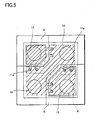
- FIG. 5 An integrated Schottky barrier diode chip of a second embodiment of this invention is described with reference to FIG. 5.
- This embodiment is similar to the first embodiment except that the second embodiment has a plurality of Schottky contact regions 11a for each of the Schottky contact barrier diodes on the chip.
- each of the two diodes has four Schottky contact regions 11a connected in parallel. Because the four Schottky contact regions 11a as a whole need to have the same Schottky contact area as the one contact area of the first embodiment, each of the Schottky contact region 11a in this embodiment has a smaller size (5 ⁇ m).
- n and n+ epitaxial layers are formed on an undoped GaAs substrate 1, as shown in FIG. 6A.
- the n+ epitaxial layer 2 (Si + 5 x 10 18 cm -3 ), which has a thickness of about 500 nm, is first formed on the undoped GaAs substrate 1 using metal-organic chemical vapor deposition (MOCVD) technique.
- MOCVD metal-organic chemical vapor deposition
- the n epitaxial layer 3 Si + 1.3 x 10 17 cm -3 ), which has a thickness of about 250 nm, is then formed on the n+ epitaxial layer using MOCVD.
- an insulating region 6 is formed in the n and n+ epitaxial layers by ion implantation technique, as shown in FIG. 6B.
- a photoresist layer (not shown) is formed on the nitride film 5. The photoresist layer is, then, exposed so that the portions of the photoresist layer that correspond to locations for formation of an insulating region 6 are removed during a subsequent developing process.
- impurities such as boron (B + ) and hydrogen (H + ) are ion-implanted into the n and n+ epitaxial layers 2, 3 using the photoresist layer as a mask.
- the ion implantation condition in this embodiment, is B + 160 KeV and 4 x 10 13 cm -2 .
- the insulating region 6 thus formed reaches the undoped GaAs substrate 1. Because the formation of the insulating region 6 does not require the trench formation of the conventional device of FIG. 2, a method of manufacturing a discrete diode device is applied to this manufacturing method without major modification.
- n type impurities are implanted into the n epitaxial layer 3 and the n+ epitaxial layer 2 to form the impurity regions 7.
- Si + impurities are implanted to provide an impurity concentration of about 1 x 10 18 cm -3 .
- the ion implantation should be performed over several implantation steps with different implantation conditions so that the impurity concentration is homogeneous along the depth direction of the impurity region 7.
- the first implantation is performed under Si + 180 KeV and 1 x 10 14 cm -2
- the second implantation is performed under Si + 30 KeV and 1 x 10 13 cm -2
- an additional nitride film 5 is formed on the nitride film 5 for annealing the impurity region 7 and the insulating region 6.
- an ohmic electrode 8 is formed on the impurity region 7 to form an ohmic contact with the impurity region 7.
- a photoresist layer is formed on the entire top surface of the device intermediate and is patterned to open portions of the photoresist layer that correspond to locations of formation of the ohmic electrode 8.
- the photoresist layer as a mask, the nitride film 5 that is exposed in the opening of the photoresist layer is removed to expose the impurity region 7.
- a first metal layer mad of AuGe/Ni/Au is deposited on the exposed surface of the impurity region 7 by vacuum-vapor depositing AuGe, Ni and Au in this order, and the photoresist layer is removed to leave the first metal layer only on the predetermined locations of the ohmic electrode 8.
- the device intermediate is, then, heated to alloy the first metal layer so that an ohmic contact is formed between the fist metal layer and the impurity region 7.
- a photoresist layer is formed on the nitride film 5 and patterned to open portions of the photoresist layer that correspond to locations of formation of Schottky contact regions 11a and the bonding pad regions.
- the portions of the nitride film 5, which is exposed in the opening of the photoresist layer, is removed by dry etching. After removal of the photoresist layer, a contact hole 9 emerges to expose the n epitaxial layer 3.
- a second metal layer 16 is formed to provide a common electrode 16a, an anode electrode 16c and a cathode electrode 16b.
- a photoresist layer is formed on the entire device intermediate and patterned to open portions of the photoresist layer that correspond to locations of formation of the electrodes 16a, 16b, 16c.
- the second metal layer 16 made of Ti/Pt/Au is, then, formed on the entire top surface of the device intermediate by vacuum-vapor depositing Ti, Pt and Au in this order. The photoresist layer is removed to leave the second metal layer 16 only at locations of the electrodes 16a, 16b, 16c.
- a Schottky contact is formed between the second metal layer 16 and the n epitaxial layer 3 at the anode portion of the diode, and an contact is formed between the second meal layer 16 and the ohmic electrode 8. Then, the backside of the substrate undergoes a back wrapping process.
- etching of the epitaxial layers 22, 23 and the GaAs substrate 21 is required to adjust the depth of the operation layer 23, to create the mesa structure and to create the trenches 26.
- the etching of the operation layer 23 is difficult to control because of the process parameters such as swing speed and swing amplitude of the device intermediate in an etching solution as well as maintenance of the etching solution.
- the planar configuration of the device of this embodiment removes the etching step of the epitaxial layers and the GaAs substrate, which is required in manufacturing the conventional integrated Schottky barrier diode chip. Accordingly, an integrated Schottky barrier diode chip with improved device characteristics is obtained.
- the conventional manufacturing method need to perform a plurality of polymer coatings for forming the polyimide layer 30 and an extended plating process for forming the tall Au plating layer 36 that is required to accommodate the low mechanical strength of the polyimide layer 30.
- the manufacturing method of this embodiment is simpler and more effective than the conventional method.
- the integrated Schottky barrier diode chips thus formed on the GaAs substrate are transferred to an assembly process.
- the GaAs wafer is diced to separate the individual chips.
- the wire bonding regions of the electrodes are connected to corresponding leads by stitch-bonding a thin gold wire line.
- a resin transfer molding of the chip and the frame completes packaging of the device.
Abstract
Description
- This invention relates to an integrated Schottky barrier diode chip made of a compound semiconductor for use in a high frequency circuit, specifically to an integrated Schottky barrier diode chip that includes an insulating region electrically separating portions of a diode of the chip, and a manufacturing method thereof.
- The demand for high frequency devices has been increasing in recent years because of the worldwide expansion of the portable telephone market as well as the increased demand for digital satellite receiving/sending equipment. Many of these devices utilize a field effect transistor (FET) made of a compound semiconductor, such as gallium arsenide (GaAs), which is suitable for use in a high frequency range. Typical example of such devices include a monolithic microwave integrated circuit (MMIC) that integrates the FETs, a local oscillation FET and a GaAs-based Schottky barrier diode that is used for sending/receiving station in wireless communication.
- FIG. 1A is a plan view of a conventional integrated Schottky barrier diode chip, and FIG 1B is its equivalent circuit. This type of integrated Schottky barrier diode is referred to as a Tee type, and has two Schottky
barrier diodes common electrode 36a and itsrelated terminal 34, acathode electrode 36b and itsrelated terminal 35, and ananode electrode 36c and itsrelated terminal 32. Theseelectrodes - The two
Schottky barrier diodes common electrode 36a. In other words, thecommon electrode 36a serves as a cathode electrode of theSchottky barrier diode 40a, the anode of which is theanode electrode 36c, and serves as an anode of theSchottky barrier diode 40b, the cathode of which is thecathode electrode 36b. The terminals are the areas of the corresponding electrodes that are used for external connection. Typically, those are the areas for wire bonding, and indicated by the circles in FIG. 1A. - This configuration provides a circuit shown in FIG. 1B. Namely, the cathode of the
Schottky barrier diode 40a, the anode of which is theanode terminal 32, is connected to the anode of theSchottky barrier diode 40b, the cathode of which is thecathode terminal 35. - FIG. 2 is a cross-sectional view of the integrated Schottky barrier diode chip of FIG. 1A. This cross-section is along the arrow in FIG. 1 and intersects operation areas of the two diodes. An n+ epitaxial layer 22 (Si+ 5 x 1018 cm-3) is disposed on an
undoped GaAs substrate 21 and has a thickness of about 6 µm. An n epitaxial layer 23 (Si+ 1.3 x 1017 cm-3) is disposed on the n+epitaxial layer 22 and has a thickness of about 350 nm. This nepitaxial layer 23 serves as an operation layer of the Schottky barrier diodes. Anohmic electrode 28 is a disposed directly on the n+epitaxial layer 22 and forms an ohmic contact with the n+epitaxial layer 22. This first metal layer is made of a AuGe/Ni/Au composite metal layer. Asecond metal layer 33, made of Ti/Pt/Au composite layer, forms a Schottky contact with the nepitaxial layer 23 in a Schottkycontact region 31a of the anode portion of the diode, and forms a contact with theohmic electrode 28 in the cathode portion of the diode. Athird metal layer 36 is a Au metal layer, which is formed by plating using thesecond metal layer 33 as a base electrode, and completely covers thesecond metal layer 33.Portions third metal layer 36 serve as thecommon electrode 36a, thecathode electrode 36b and theanode electrode 36c, respectively. - The Schottky
contact region 31a has a circular shape with a diameter of about 10 µm, as shown in FIG. 1. Thefirst metal layer 28 surrounds the Schottkycontact region 31a. The first and second metal layers are formed by vapor depositing the constituent metals separately. In theterminal areas corresponding electrodes reference numerals - In the configuration of FIG. 2, the Schottky barrier diode on the left 40b has the
cathode electrode 36b, which serves a cathode of this left diode and thecommon electrode 36a, which serves as an anode of this left diode, and the Schottky barrier diode on the right 40a has theanode electrode 36c, which serves an anode of this right diode and thecommon electrode 36a, which serves as a cathode of this right diode. Accordingly, thecommon electrode 36a works as an anode electrode of thediode 40b and a cathode electrode of thediode 40a. Furthermore, thesecond metal layer 33 on the Schottkycontact regions 31a is at an anode voltage, and the n+ and n epitaxial layers are at a cathode voltage. In this structure, apolyimide layer 30 is required as an insulating layer under the second andthird metal layers metal layers epitaxial layers polyimide layer 30 needs to be as much as 6-7 µm because this intersection area is large and the resultant parasitic capacitance must be reduced by increasing the thickness. Polyimide is used as the insulating layer because it has a low dielectric constant and suitable for a thick layer formation. - Furthermore, this configuration needs a
trench 26 that separates the portions of theepitaxial layers epitaxial layers trenches 26 reach the undopedgallium arsenide substrate 21, and are filled with the same polyimide used for thepolyimide layer 30. Theohmic electrode 28 needs to form a direct contact with the n+ epitaxial layer for reducing the associated electric resistance. For this reason, a mesa etching is required to expose the n+epitaxial layer 22 that is covered by the nepitaxial layer 23. The nepitaxial layer 23 at the Schottky contact region is also required to be etched to precisely the thickness of 250 nm for good electric characteristics. - However, the Schottky barrier diode of the conventional configuration described above has a few disadvantages. First, further size reduction of the device is difficult because such a configuration needs a large positional error margin for absorbing mask misplacement during manufacturing due to the tall polyimide layer (6-7 µm) and the deep trenches (15 µm). Second, the trench structure requires an additional process step exclusively designed for trench formation, which needs to be added to a manufacturing method of a discrete device.
- The object of this invention is directed to an integrated Schottky barrier diode chip that is smaller and is fabricated by a simpler process than the conventional integrated Schottky barrier diode chip.
- The solution according to the invention lies in the features of the independent claim and preferably in those of the dependent claims.
- The invention provides an integrated Schottky barrier diode chip including a compound semiconductor substrate, an operation layer formed on the substrate, and a plurality of Schottky barrier diodes formed on the substrate. The device also includes an insulating region formed in the operation layer, which electrically separates a first portion of the operation layer of one of the plurality of Schottky barrier diodes from a second portion of the operation layer of that Schottky barrier diodes. The device further includes an impurity region formed in the operation layer, which electrically communicates with one of the first and second portions of the operation layer of that Schottky barrier diode.
- The invention also provides an integrated Schottky barrier diode chip that has a first Schottky barrier diode and a second Schottky barrier diode each formed on a compound semiconductor substrate. The device includes an operation layer formed on the substrate, an anode electrode, a cathode electrode and a common electrode. A first insulating region and a first impurity region are formed in the operation layer for the first Schottky barrier diode. A second insulating region and a second impurity region are formed in the operation layer for the second Schottky barrier diode. In this configuration, the first insulating region electrically separates a portion of the operation layer of the first diode that is connected to the anode electrode from a portion of the operation layer of the first diode that is connected to the common electrode, and the second insulating region electrically separates a portion of the operation layer of the second diode that is connected to the common electrode from a portion of the operation layer of the second diode that is connected to the cathode electrode. The first impurity region electrically communicates with the operation layer of the first diode that is connected to the common electrode, and the second impurity region electrically communicates with the operation layer of the second diode that is that is connected to the cathode electrode.
- The invention further provides a method of manufacturing an integrated Schottky barrier diode chip having a plurality of Schottky barrier diodes. The method includes forming a plurality of insulating regions on a compound semiconductor substrate by an ion implantation, and forming a Schottky barrier diode on each of the plurality of the insulating regions so that each of the insulating regions electrically separates a first portion of the corresponding diode from a second portion of the corresponding diode.
- The invention also provides a method of manufacturing an integrated Schottky barrier diode chip having a plurality of Schottky barrier diodes. The method includes forming an epitaxial layer of a conduction type on an undoped compound semiconductor substrate, forming a plurality of insulating regions in the epitaxial layer by an ion implantation, and forming a Schottky barrier diode on each of the plurality of the insulating regions so that each of the insulating regions electrically separates a first portion of the epitaxial layer of the corresponding diode from a second portion of the epitaxial layer of the corresponding diode.
-
- FIG. 1A is a plan view of a conventional integrated Schottky barrier diode chip with two diodes, and FIG. 1B is an equivalent circuit of the device of FIG. 1A.
- FIG. 2 is a cross-sectional view of the conventional device of FIG. 1A cut along the arrow shown in FIG. 1A.
- FIG. 3A is a plan view of an integrated Schottky barrier diode chip with two diodes of a first embodiment of this invention, and FIG. 3B is an equivalent circuit of the device of FIG. 3A.
- FIG. 4 is a cross-sectional view of the device of the first embodiment cut along the arrow shown in FIG. 3A.
- FIG. 5 is a cross-sectional view of an integrated Schottky barrier diode chip with two diodes of a second embodiment of this invention.
- FIGS. 6A-6D show cross-sectional views of device intermediates at process steps of a manufacturing method of the integrated Schottky barrier diode chip of the first embodiment.
-
- Two embodiments of this invention will be described with reference to FIGS. 3-6D. Both of the embodiments include an
undoped GaAs substrate 1, ananode electrode 16c, acathode electrode 16b, acommon electrode 16a,Schottky barrier diodes insulating region 6. - A first embodiment of this invention is described with reference to FIGS. 3A, 3B, 4. FIG. 3A is a plan view of an integrated Schottky barrier diode chip of the first embodiment of this invention, and FIG. 3B is an equivalent circuit of the device of FIG. 3A. This integrated Schottky barrier diode is a Tee type device, and has two
Schottky barrier diodes common electrode 16a and itsrelated terminal 14, acathode electrode 16b and itsrelated terminal 15, and ananode electrode 16c and itsrelated terminal 12. Theseelectrodes - The two
Schottky barrier diodes common electrode 16a. In other words, thecommon electrode 16a serves as a cathode of theSchottky barrier diode 20a, the anode of which is theanode electrode 16c, and serves as an anode of theSchottky barrier diode 20b, the cathode of which is thecathode electrode 16b. The terminals are the areas of the corresponding electrodes that are used for external connection. Typically, those are the areas for wire bonding, and indicated by the circles in FIG. 3A. - This configuration provides a circuit shown in FIG. 3B. Namely, the cathode of the
Schottky barrier diode 20a, the anode of which is theanode terminal 12, is connected to the anode of theSchottky barrier diode 20b, the cathode of which is thecathode terminal 15. - FIG. 4 is a cross-sectional view of the integrated Schottky barrier diode chip of FIG. 3A. This cross-section is along the arrow in FIG. 3A and intersects operation areas of the two diodes. An n+ epitaxial layer 2 (Si+ 5 x 1018 cm-3) is disposed on an
undoped GaAs substrate 1 and has a thickness of about 500 nm. An n epitaxial layer 3 (Si+ 1.3 x 1017 cm-3) is disposed on then+ epitaxial layer 2 and has a thickness of about 250 nm. This nepitaxial layer 3 is an operation layer of the Schottky barrier diodes. -
Impurity region 7 of a high concentration (Si+ 1 x 1018 cm-3) is formed in then epitaxial layer 3 under anohmic electrode 8, and reaches then+ epitaxial layer 2. Theimpurity region 7 surrounds aSchottky contact region 11a, which is circular as shown in FIG. 3A, and overlaps with theohmic electrode 8, which is indicated by the area encircled by the broken lines in FIG. 3A. In the region surrounding theSchottky contact region 11a, theimpurity region 7 is larger than theohmic electrode 8 and extends outside the area covered by theohmic electrode 8. The distance between the edge of theSchottky contact region 11a and the edge of theimpurity region 7 is about 1 µm, and the distance between the edge of theSchottky contact region 11a and the edge of theohmic electrode 8 is about 2 µm. Because of thisimpurity region 7, which reaches then+ epitaxial layer 2 form the surface of then epitaxial layer 3, there is no need for forming a mesa structure, which is required for forming an ohmic contact with the n+ epitaxial layer in the conventional device as shown in FIG. 2. Accordingly, the device of the first embodiment has a planar configuration. - The
ohmic electrode 8 is a disposed directly on theimpurity region 7 and forms an ohmic contact with then+ epitaxial layer 2 through theimpurity region 7. This first metal layer is made of a AuGe/Ni/Au composite metal layer and has a hole corresponding to theSchottky contact region 11a, as shown by the broken line in FIG. 3A. Asecond metal layer 16, made of Ti/Pt/Au composite layer, forms a Schottky contact with then epitaxial layer 3 in theSchottky contact region 11a of the anode portion of the diode, and forms an contact with theohmic electrode 8 in the cathode portion of the diode.Portions second metal layer 16 serve as thecommon electrode 16a, thecathode electrode 16b and theanode electrode 16c, respectively. - The
Schottky contact region 11a has a circular shape with a diameter of about 10 µm, as shown in FIG. 3A. The thickness (250 nm) of then epitaxial layer 3, which is an operation layer of the Schottky barrier diode, is determined so that proper device characteristics, including a high breakdown voltage, are obtained. Because of the planar configuration of this embodiment, the thickness control of the operation layer or the mesa etching is not needed. Then the device of the first embodiment is much easier to produce and more reliable than the conventional device that requires very precise etching control of the operation layer and complicated mesa etching. Accordingly, the integrated Schottky barrier diode chip of this embodiment has improved device characteristics. - The
common electrode 16a is disposed diagonally on the chip, and two areas for wire bonding are provided at both diagonal ends of the common electrode. Only one area needs to be wire-bonded for external connection and become acommon terminal 14. This configuration makes it easier to mount the integrated Schottky barrier diode chip of this embodiment on a package frame, a print board or the like, because thecommon electrode 16a is accessible from two different directions for wire bonding. - In the configuration of FIG. 4, the
Schottky barrier diode 20a on the left has theanode electrode 16c, which serves as an anode of this left diode and thecommon electrode 16a, which serves as a cathode of this left diode, and theSchottky diode 20b on the right has thecathode electrode 16b, which serves as a cathode of this right diode and thecommon electrode 16a, which serves as an anode of this right diode. Accordingly, thecommon electrode 16a works as a cathode electrode of thediode 20a and an anode electrode of thediode 20b. Furthermore, thesecond metal layer 16 on theSchottky contact regions 11a is at an anode voltage, and the n+ and n epitaxial layers are at a cathode voltage. - An
insulating region 6 is formed for each of the anode andcathode electrodes electrodes diodes layer 6 electrically separates the portions of the n+ and n epitaxial layers 2, 3 that are at the anode voltage form the portions of the n+ and n epitaxial layers 2, 3 that are at the cathode voltage. For this purpose, each of the insulatingregions 6 reaches theundoped GaAs substrate 1, which is essentially an insulating substrate. Theinsulating region 6 replaces the conventional trench structure of FIG. 2. - An insulating
film 5, made of silicon nitride, prevents the portions of thesecond metal layer 16 that are at the anode voltage from contacting the portion of the n+ and n epitaxial layers and correspondingimpurity regions 7 that are at the cathode voltage. This insulatingfilm 5 replaces the conventional polyimide layer of FIG. 2. Although the siliconnitride insulating film 5 is thinner and has a higher dielectric constant than the polyimide layer of the conventional device, it can be used as an insulating layer because it occupies a smaller area than the conventional polyimide layer. - In other words, in this configuration, the area of the intersection between the
second metal layer 16 that is at the anode voltage and the portion of the n and n+epitaxial layers impurity regions 6 that are at the cathode voltage are much smaller than that of the conventional device. This is made possible thanks to the smaller process error margin due to the planar configuration of this embodiment, which are free from the mesa structure and the tall polyimide insulating layer that require larger process error margin and, thus, a larger separation between the Schottky contact region and the ohmic electrode, which results in a larger area for generating parasitic capacitance. - The distance between the edge of the
Schottky contact region 11a and the edge of theohmic electrode 8 in this embodiment is 2 µm, which is much shorter than 7 µm, the corresponding distance of the conventional device. Furthermore, the distance between the edge of theSchottky region 11a and the edge of theimpurity region 7 is 1 µm. Since theimpurity region 7, which serves as a carrier path, has the electronic conduction properties similar to theohmic electrode 8, the effective separation in this embodiment is about one seventh of the conventional device. This shorter separation also contributes to reduction of the electric resistance between theSchottky contact region 11a and theohmic electrode 8/impurity region 7, and thus improvement of high frequency device characteristics. - The configuration described above does not have a deep trench or tall polyimide layer on the surface of the GaAs chip. Accordingly, the accuracy of positioning masks for patterning is improved and the large processing error margins for patterning is not required for manufacturing the integrated Schottky barrier diode chip of this invention. Furthermore, the absence of the polyimide layer removes the requirements for tapering the side of the polyimide layer and the related process error margin for the tapered side. Because of this reduction of the error margins, the chip size of this embodiment is significantly reduced. The reduced error margin also allows size reduction in the operation area of the diode, which includes the
Schottky contact region 11a and the correspondingohmic electrode 8. This, in turn, provides a more flexible device design, in which the location of the two diodes are determined based on other device design requirements. Taking advantage of this flexible design feature, thecommon electrode 16a is disposed diagonally on the chip in this embodiment, as described earlier. - An integrated Schottky barrier diode chip of a second embodiment of this invention is described with reference to FIG. 5. This embodiment is similar to the first embodiment except that the second embodiment has a plurality of
Schottky contact regions 11a for each of the Schottky contact barrier diodes on the chip. In the device shown in FIG. 5, each of the two diodes has fourSchottky contact regions 11a connected in parallel. Because the fourSchottky contact regions 11a as a whole need to have the same Schottky contact area as the one contact area of the first embodiment, each of theSchottky contact region 11a in this embodiment has a smaller size (5 µm). In this configuration, carrier trap efficiency in theimpurity region 7 becomes higher because the separation between the center of theSchottky contact region 11a and theimpurity region 7 is further reduced. This leads to a reduced cathode resistance and, thus, improved high frequency device characteristics. - A manufacturing method of the device of the first embodiment will be described below with reference to FIGS. 6A-6D. First, n and n+ epitaxial layers are formed on an
undoped GaAs substrate 1, as shown in FIG. 6A. The n+ epitaxial layer 2 (Si+ 5 x 1018 cm-3), which has a thickness of about 500 nm, is first formed on theundoped GaAs substrate 1 using metal-organic chemical vapor deposition (MOCVD) technique. The n epitaxial layer 3 (Si+ 1.3 x 1017 cm-3), which has a thickness of about 250 nm, is then formed on the n+ epitaxial layer using MOCVD. - In the next process step, an
insulating region 6 is formed in the n and n+ epitaxial layers by ion implantation technique, as shown in FIG. 6B. First, the entire top surface of the device intermediate of FIG. 6A is covered by anitride film 5, and a photoresist layer (not shown) is formed on thenitride film 5. The photoresist layer is, then, exposed so that the portions of the photoresist layer that correspond to locations for formation of aninsulating region 6 are removed during a subsequent developing process. After the developing of the photoresist layer, impurities such as boron (B+) and hydrogen (H+) are ion-implanted into the n and n+epitaxial layers insulating region 6 thus formed reaches theundoped GaAs substrate 1. Because the formation of theinsulating region 6 does not require the trench formation of the conventional device of FIG. 2, a method of manufacturing a discrete diode device is applied to this manufacturing method without major modification. - After removal of the photoresist layer, another photoresist layer is formed on the entire device intermediate. This photoresist layer is patterned to provide openings that correspond to locations of formation of
impurity regions 7. Using this photoresist layer as a mask, n type impurities are implanted into then epitaxial layer 3 and then+ epitaxial layer 2 to form theimpurity regions 7. In this embodiment, Si+ impurities are implanted to provide an impurity concentration of about 1 x 10 18 cm-3. The ion implantation should be performed over several implantation steps with different implantation conditions so that the impurity concentration is homogeneous along the depth direction of theimpurity region 7. For example, in this embodiment, the first implantation is performed under Si+ 180 KeV and 1 x 10 14 cm-2, and the second implantation is performed underSi + 30 KeV and 1 x 10 13 cm-2. After removal of the photoresist layer, anadditional nitride film 5 is formed on thenitride film 5 for annealing theimpurity region 7 and theinsulating region 6. - In the process step shown in FIG. 6C, an
ohmic electrode 8 is formed on theimpurity region 7 to form an ohmic contact with theimpurity region 7. First, a photoresist layer is formed on the entire top surface of the device intermediate and is patterned to open portions of the photoresist layer that correspond to locations of formation of theohmic electrode 8. Using the photoresist layer as a mask, thenitride film 5 that is exposed in the opening of the photoresist layer is removed to expose theimpurity region 7. A first metal layer mad of AuGe/Ni/Au is deposited on the exposed surface of theimpurity region 7 by vacuum-vapor depositing AuGe, Ni and Au in this order, and the photoresist layer is removed to leave the first metal layer only on the predetermined locations of theohmic electrode 8. The device intermediate is, then, heated to alloy the first metal layer so that an ohmic contact is formed between the fist metal layer and theimpurity region 7. This configuration of theimpurity region 7 and theohmic electrode 8 enables the planar structure of the integrated Schottky barrier diode chip of this embodiment. - Then, an
additional nitride film 5, which has a thickness of about 500 nm, is formed on the entire device intermediate. A photoresist layer is formed on thenitride film 5 and patterned to open portions of the photoresist layer that correspond to locations of formation ofSchottky contact regions 11a and the bonding pad regions. The portions of thenitride film 5, which is exposed in the opening of the photoresist layer, is removed by dry etching. After removal of the photoresist layer, acontact hole 9 emerges to expose then epitaxial layer 3. - In the process step shown in FIG. 6D, a
second metal layer 16 is formed to provide acommon electrode 16a, ananode electrode 16c and acathode electrode 16b. A photoresist layer is formed on the entire device intermediate and patterned to open portions of the photoresist layer that correspond to locations of formation of theelectrodes second metal layer 16 made of Ti/Pt/Au is, then, formed on the entire top surface of the device intermediate by vacuum-vapor depositing Ti, Pt and Au in this order. The photoresist layer is removed to leave thesecond metal layer 16 only at locations of theelectrodes second metal layer 16 and then epitaxial layer 3 at the anode portion of the diode, and an contact is formed between thesecond meal layer 16 and theohmic electrode 8. Then, the backside of the substrate undergoes a back wrapping process. - In the conventional manufacturing method of the device shown in FIG. 1A, etching of the
epitaxial layers GaAs substrate 21 is required to adjust the depth of theoperation layer 23, to create the mesa structure and to create thetrenches 26. Especially, the etching of theoperation layer 23 is difficult to control because of the process parameters such as swing speed and swing amplitude of the device intermediate in an etching solution as well as maintenance of the etching solution. The planar configuration of the device of this embodiment removes the etching step of the epitaxial layers and the GaAs substrate, which is required in manufacturing the conventional integrated Schottky barrier diode chip. Accordingly, an integrated Schottky barrier diode chip with improved device characteristics is obtained. - Furthermore, the conventional manufacturing method need to perform a plurality of polymer coatings for forming the
polyimide layer 30 and an extended plating process for forming the tallAu plating layer 36 that is required to accommodate the low mechanical strength of thepolyimide layer 30. By replacing the polyimide layer with the thin nitride film and replacing the Au plating layer with the thin vapor-deposited metal layer, the manufacturing method of this embodiment is simpler and more effective than the conventional method. - Finally, the integrated Schottky barrier diode chips thus formed on the GaAs substrate are transferred to an assembly process. The GaAs wafer is diced to separate the individual chips. After the separated chips are mounted on a frame, the wire bonding regions of the electrodes are connected to corresponding leads by stitch-bonding a thin gold wire line. A resin transfer molding of the chip and the frame completes packaging of the device.
Claims (19)
- An integrated Schottky barrier diode chip comprising:a compound semiconductor substrate (1);an operation layer (3) formed on the substrate (1);a plurality of Schottky barrier diodes (20a, 20b) formed on the substrate (1);an insulating region (6) formed in the operation layer (3), the insulating region (6) electrically separating a first portion of the operation layer of one of the plurality of Schottky barrier diodes (20a, 20b) from a second portion of the operation layer of said one of the plurality of Schottky barrier diodes (20a, 20b); andimpurity region (7) formed in the operation layer (3), the impurity region (7) electrically communicating with one of the first and second portions of the operation layer (3) of said one of the plurality of Schottky barrier diodes (20a, 20b).
- The integrated Schottky barrier diode chip of claim 1, wherein the first portion receives a cathode voltage and the second portion receive an anode voltage.
- The integrated Schottky barrier diode chip of claim 1 or 2, wherein an electrode (16a) of said one of the plurality of Schottky barrier diodes (20a) is connected to an electrode of another of the plurality of Schottky barrier diodes (20b).
- The integrated Schottky barrier diode chip according to any of claims 1 to 3, wherein the compound semiconductor substrate (1) is made of an undoped gallium arsenide, the operation layer comprises an epitaxial layer (3) of a conduction type, and said one of the plurality of Schottky barrier diodes (20a, 20b) comprises an ohmic electrode (8) formed on the epitaxial layer (3) and an electrode forming a Schottky contact with the epitaxial layer (3).
- The integrated Schottky barrier diode chip of claim 3, wherein the insulating region (6) reaches the undoped gallium arsenide substrate (1).
- The integrated Schottky barrier diode chip according to any of claims 1 to 5, wherein the insulating region (6) is formed by an ion implantation.
- The integrated Schottky barrier diode chip according to any of claims 1 to 6, wherein said one of the plurality of Schottky barrier diodes (20a, 20b) comprises a plurality of Schottky contact regions (11a).
- An integrated Schottky barrier diode chip including a first Schottky barrier diode and a second Schottky barrier diode each formed on a compound semiconductor substrate (1), the chip comprises:an operation layer (3) formed on the substrate (1);an anode electrode;a cathode electrode;a common electrode;a first insulating region (6) and a first impurity region (7) each formed in the operation layer (3) for the first Schottky barrier diode; anda second insulating region (6) and a second impurity region (7) each formed in the operation layer (3) for the second Schottky barrier diode, whereinthe first insulating region (6) electrically separates a portion of the operation layer (3) of the first diode (20a) that is connected to the anode electrode (16c) from a portion of the operation layer (3) of the first diode (20a) that is connected to the common electrode (16a), and the second insulating region (6) electrically separates a portion of the operation layer (3) of the second diode (20b) that is connected to the common electrode (16a) from a portion of the operation layer (3) of the second diode (20b) that is connected to the cathode electrode (16b), andthe first impurity region (7) electrically communicates with the operation layer (3) of the first diode (20a) that is connected to the common electrode (16a), and the second impurity region (7) electrically communicates with the operation layer (3) of the second diode (20b) that is connected to the cathode electrode (16b).
- The integrated Schottky barrier diode chip of claim 8, wherein the common electrode (16a) serves as a cathode electrode of the first diode (20a) and an anode electrode of the second diode (20b).
- The integrated Schottky barrier diode chip of claim 9, wherein the common electrode (16a) is disposed diagonally on the substrate and provides two areas for wire bonding.
- The integrated Schottky barrier diode chip according to any of claims 8 to 10, wherein the compound semiconductor substrate (1) is made of an undoped gallium arsenide, the operation layer comprises an epitaxial layer (3) of a conduction type, and each of the first and second diodes (20a, 20b) comprises an ohmic electrode (8) formed on the epitaxial layer (3) and an electrode forming a Schottky contact with the epitaxial layer (3).
- The integrated Schottky barrier diode chip of claim 11, wherein the first and second insulating regions (6) reach the undoped gallium arsenide substrate (1).
- The integrated Schottky barrier diode chip according to any of claims 8 to 12, wherein each of the first and second diodes (20a, 20b) comprises a plurality of Schottky contact regions (11a).
- The integrated Schottky barrier diode chip according to any of claims 8 to 13, wherein the first and second insulating regions (6) are formed by an ion implantation.
- A method of manufacturing an integrated Schottky barrier diode chip comprising a plurality of Schottky barrier diodes, the method comprising:forming a plurality of insulating regions (6) on a compound semiconductor substrate (1) by an ion implantation; andforming a Schottky barrier diode (20a, 20b) on each of the plurality of the insulating regions (6) so that each of the insulating regions (6) electrically separates a first portion of the corresponding diode (20a, 20b) from a second portion of the corresponding diode (20a, 20b).
- The method of manufacturing an integrated Schottky barrier diode chip of claim 15, wherein the forming of the Schottky barrier diode (20a, 20b) comprises forming a plurality of Schottky contacts.
- A method of manufacturing an integrated Schottky barrier diode chip comprising a plurality of Schottky barrier diodes, the method comprising:forming an epitaxial layer (3) of a conduction type on an undoped compound semiconductor substrate (1);forming a plurality of insulating regions (6) in the epitaxial layer (3) by an ion implantation;forming a Schottky barrier diode (20a, 20b) on each of the plurality of the insulating regions (6) so that each of the insulating regions (6) electrically separates a first portion of the epitaxial layer (3) of the corresponding diode (20a, 20b) from a second portion of the epitaxial layer (3) of the corresponding diode (20a, 20b).
- The method of manufacturing an integrated Schottky barrier diode chip of claim 17, wherein the forming of the Schottky barrier diode (20a, 20b) comprises forming a plurality of Schottky contacts.
- An integrated Schottky barrier diode chip comprising:a compound semiconductor substrate (1);a plurality of Schottky barrier diodes (20a, 20b) formed on the substrate (1); andan insulating region (6) formed on the substrate (1), the insulating region (6) electrically separating a first portion of one of the plurality of Schottky barrier diodes (20a, 20b) from a second portion of said one of the plurality of Schottky barrier diodes (20a, 20b), the insulating region (6) being formed by an ion implantation.
Applications Claiming Priority (2)
| Application Number | Priority Date | Filing Date | Title |
|---|---|---|---|
| JP2001334087A JP2003142697A (en) | 2001-10-31 | 2001-10-31 | Integrated schottky barrier diode and manufacturing method thereof |
| JP2001334087 | 2001-10-31 |
Publications (2)
| Publication Number | Publication Date |
|---|---|
| EP1309012A2 true EP1309012A2 (en) | 2003-05-07 |
| EP1309012A3 EP1309012A3 (en) | 2005-04-20 |
Family
ID=19149274
Family Applications (1)
| Application Number | Title | Priority Date | Filing Date |
|---|---|---|---|
| EP20020024472 Withdrawn EP1309012A3 (en) | 2001-10-31 | 2002-10-29 | Integrated Schottky barrier diode and manufacturing method thereof |
Country Status (6)
| Country | Link |
|---|---|
| US (1) | US6787871B2 (en) |
| EP (1) | EP1309012A3 (en) |
| JP (1) | JP2003142697A (en) |
| KR (1) | KR100620926B1 (en) |
| CN (1) | CN100472814C (en) |
| TW (1) | TW561623B (en) |
Families Citing this family (8)
| Publication number | Priority date | Publication date | Assignee | Title |
|---|---|---|---|---|
| US7528459B2 (en) * | 2003-05-27 | 2009-05-05 | Nxp B.V. | Punch-through diode and method of processing the same |
| JP4637553B2 (en) * | 2004-11-22 | 2011-02-23 | パナソニック株式会社 | Schottky barrier diode and integrated circuit using the same |
| DE102004056663A1 (en) * | 2004-11-24 | 2006-06-01 | Robert Bosch Gmbh | Semiconductor device and rectifier arrangement |
| JP4567426B2 (en) * | 2004-11-25 | 2010-10-20 | パナソニック株式会社 | Schottky barrier diode and diode array |
| JP5044986B2 (en) * | 2006-05-17 | 2012-10-10 | サンケン電気株式会社 | Semiconductor light emitting device |
| EP2454760A2 (en) * | 2009-07-17 | 2012-05-23 | Lockheed Martin Corporation | Strain-balanced extended-wavelength barrier photodetector |
| KR101051578B1 (en) * | 2009-09-08 | 2011-07-22 | 삼성전기주식회사 | Semiconductor device and manufacturing method thereof |
| CN102184853B (en) * | 2011-05-06 | 2015-12-02 | 上海华虹宏力半导体制造有限公司 | The manufacture method of Schottky diode |
Citations (2)
| Publication number | Priority date | Publication date | Assignee | Title |
|---|---|---|---|---|
| DE3620686A1 (en) * | 1986-06-20 | 1987-12-23 | Licentia Gmbh | Structured semiconductor body |
| US4745445A (en) * | 1983-03-15 | 1988-05-17 | Itt Gallium Arsenide Technology Center, A Division Of Itt Corporation | Interdigitated Schottky diode |
Family Cites Families (6)
| Publication number | Priority date | Publication date | Assignee | Title |
|---|---|---|---|---|
| US4254428A (en) * | 1979-12-28 | 1981-03-03 | International Business Machines Corporation | Self-aligned Schottky diode structure and method of fabrication |
| JPS59161836A (en) * | 1983-03-04 | 1984-09-12 | Sanyo Electric Co Ltd | Semiconductor device |
| US5021840A (en) * | 1987-08-18 | 1991-06-04 | Texas Instruments Incorporated | Schottky or PN diode with composite sidewall |
| FR2650439B1 (en) * | 1989-07-27 | 1991-11-15 | Sgs Thomson Microelectronics | VDMOS / LOGIC INTEGRATED CIRCUIT INCLUDING A DIODE |
| JP3093620B2 (en) * | 1995-10-19 | 2000-10-03 | 日本電気株式会社 | Method for manufacturing semiconductor device |
| JP2003101036A (en) * | 2001-09-25 | 2003-04-04 | Sanyo Electric Co Ltd | Schottky barrier diode and manufacturing method therefor |
-
2001
- 2001-10-31 JP JP2001334087A patent/JP2003142697A/en active Pending
-
2002
- 2002-10-17 TW TW91123897A patent/TW561623B/en not_active IP Right Cessation
- 2002-10-29 EP EP20020024472 patent/EP1309012A3/en not_active Withdrawn
- 2002-10-30 KR KR20020066501A patent/KR100620926B1/en not_active IP Right Cessation
- 2002-10-30 US US10/283,331 patent/US6787871B2/en not_active Expired - Lifetime
- 2002-10-30 CN CNB02147950XA patent/CN100472814C/en not_active Expired - Fee Related
Patent Citations (2)
| Publication number | Priority date | Publication date | Assignee | Title |
|---|---|---|---|---|
| US4745445A (en) * | 1983-03-15 | 1988-05-17 | Itt Gallium Arsenide Technology Center, A Division Of Itt Corporation | Interdigitated Schottky diode |
| DE3620686A1 (en) * | 1986-06-20 | 1987-12-23 | Licentia Gmbh | Structured semiconductor body |
Non-Patent Citations (2)
| Title |
|---|
| DICK G W ET AL: "2.4 Gb/s GaAs 8*8 time multiplexed switch integrated circuit" 11TH ANNUAL GAAS IC SYMPOSIUM. TECHNICAL DIGEST 1989, 22 October 1989 (1989-10-22), pages 101-104, XP010085923 * |
| PATENT ABSTRACTS OF JAPAN vol. 009, no. 015 (E-291), 22 January 1985 (1985-01-22) & JP 59 161836 A (SANYO DENKI KK), 12 September 1984 (1984-09-12) * |
Also Published As
| Publication number | Publication date |
|---|---|
| KR100620926B1 (en) | 2006-09-13 |
| EP1309012A3 (en) | 2005-04-20 |
| US20030094668A1 (en) | 2003-05-22 |
| TW561623B (en) | 2003-11-11 |
| US6787871B2 (en) | 2004-09-07 |
| KR20030036047A (en) | 2003-05-09 |
| CN1417867A (en) | 2003-05-14 |
| JP2003142697A (en) | 2003-05-16 |
| CN100472814C (en) | 2009-03-25 |
Similar Documents
| Publication | Publication Date | Title |
|---|---|---|
| US6627967B2 (en) | Schottky barrier diode | |
| US8294254B2 (en) | Chip scale surface mounted semiconductor device package and process of manufacture | |
| US20030025175A1 (en) | Schottky barrier diode | |
| US9887152B2 (en) | Method for manufacturing semiconductor devices having a metallisation layer | |
| KR100738149B1 (en) | Semiconductor device and manufacturing method thereof | |
| US6940157B2 (en) | High frequency semiconductor module, high frequency semiconductor device and manufacturing method for the same | |
| US20050179106A1 (en) | Schottky barrier diode | |
| US6787871B2 (en) | Integrated schottky barrier diode and manufacturing method thereof | |
| KR100612189B1 (en) | Schottky barrier diode and method of fabricating the same | |
| KR100612188B1 (en) | Schottky barrier diode and manufacturing method of the same | |
| KR100612186B1 (en) | Schottky barrier diode and method of fabricating the same | |
| US6682968B2 (en) | Manufacturing method of Schottky barrier diode | |
| KR100612187B1 (en) | Manufacturing method of schottky barrier diode | |
| KR100616049B1 (en) | Schottky barrier diode and manufacturing method thereof | |
| KR100620924B1 (en) | Schottky barrier diode and method of fabricating the same | |
| EP1280210A2 (en) | Schottky barrier diode and manufacturing method of schottky barrier diode |
Legal Events
| Date | Code | Title | Description |
|---|---|---|---|
| PUAI | Public reference made under article 153(3) epc to a published international application that has entered the european phase |
Free format text: ORIGINAL CODE: 0009012 |
|
| AK | Designated contracting states |
Designated state(s): AT BE BG CH CY CZ DE DK EE ES FI FR GB GR IE IT LI LU MC NL PT SE SK TR |
|
| AX | Request for extension of the european patent |
Extension state: AL LT LV MK RO SI |
|
| PUAL | Search report despatched |
Free format text: ORIGINAL CODE: 0009013 |
|
| AK | Designated contracting states |
Kind code of ref document: A3 Designated state(s): AT BE BG CH CY CZ DE DK EE ES FI FR GB GR IE IT LI LU MC NL PT SE SK TR |
|
| AX | Request for extension of the european patent |
Extension state: AL LT LV MK RO SI |
|
| AKX | Designation fees paid | ||
| STAA | Information on the status of an ep patent application or granted ep patent |
Free format text: STATUS: THE APPLICATION IS DEEMED TO BE WITHDRAWN |
|
| 18D | Application deemed to be withdrawn |
Effective date: 20051021 |
|
| REG | Reference to a national code |
Ref country code: DE Ref legal event code: 8566 |